
Abstract
Organometal halide perovskites have recently emerged as an appealing candidate in photovoltaic devices due to their excellent properties. Therefore, intense efforts have been devoted to find the ideal organics for perovskite solar cells. In response, we investigate the doping effect of CH3SH organic on the structure and related performance of a CH3NH3PbI3 perovskite solar cell, via in situ synchrotron-based grazing incidence X-ray diffraction (GIXRD), together with scanning electron microscopy (SEM). In situ GIXRD investigations clearly illustrated the transformation and modification of the perovskite structure induced by the organic dopant, which subsequently led to the enhancement of the power conversion efficiency of fabricated solar cells. Notably, nanoporous morphology and nanocrystalline structures were discovered in the perovskite film by SEM; they were also confirmed by the increase in broadening peaks/features in the GIXRD measurements. Overall, our study may ultimately result in an attractive strategy for the fabrication of high performance perovskite solar cells.
1. Introduction
With the aim of producing environmental friendly and energy efficient energy at low cost, various materials and methodologies have been proposed for related sustainable development. Among the measures to address energy shortages faced nowadays, solar cells have been proven to be an attractive approach towards producing green energy [1-4, 5-7]. Specifically, organic-inorganic lead halide perovskite solar cells are particularly promising for the next generation of solar devices owing to their high power conversion efficiency [8, 9]. For instance, metal halide perovskites (CH3NH3PbI3 and its analogue) are currently among the most competitive candidates in the fabrication of mesoscopic solid state solar cells with record-breaking efficiencies [10, 11]. Methylammonium (CH3NH3+) was proposed by Dieter Weber to make the first three-dimensional organic–inorganic hybrid perovskites in 1978 [12], while the successful integration of organic-inorganic metal halide perovskites into solar cells was firstly reported by Miyasaka et al. in 2009 [13]. An organic-inorganic lead halide perovskite is the material that crystallizes into an AMX3 (where A is an organic ammonium cation, M is metal, which is typically Pb or Sb, and X is a halide anion) structure. When realized, the size of cation A is critical to the formation of a close-packed perovskite structure, which means cation A must fit into the centre of the unit cell, as shown in Figure 1. Methylammonium was demonstrated to be an ideal candidate for cation A and, consequently, methylammonium lead iodide (MAPbI3) has been intensively used in solar cells with an average efficiency of around 16%-17% (and, so far, up to 19.3%) in planar device architecture, but also due to its superior band gap of about 1.5–1.6 eV and a light absorption spectrum up to a wavelength of 800 nm [13,14].

Illustration of the perovskite-structured films, where A stands for organic cation B stands for Pb atom and X stands for halide anion (Cl, Br or l)
In spite of these promising successes, there have already been considerable efforts utilizing other organics as well as cation A [15-19], in order to tune the band gap of the formed perovskite architecture and the light absorption wavelength to get more overlap with the sunlight. As expected, exciting discoveries were witnessed when slightly larger formamidinium (HC(NH2)+, here denoted as FA, was confirmed as stabilizing a perovskite structure [20-22]. The band gap of FAPbI3 was estimated to be 1.45 eV; therefore, broader absorption is expected for FAPbI3 compared to MAPbI3, which indicates that a higher PCE is expected due to a higher photocurrent. For example, an average PCE of 18.4% in an FAPbI3 solar cell was reported by Seok et al. [8], while a stable FAPbI3 perovskite structure owing 16% PCE was easily fabricated by Park et al. [20]. In addition, perovskites solar cells are required to be robust during structural transition, which may induce changes of band structures or other physics properties [21, 22]. Typical CH3NH3PbI3 perovskite films undergo reversible phase transition between tetragonal and cubic symmetry at temperatures ranging from 300 to 400 K [10], which exactly correspond to a solar cell operating temperature. Based on these considerations, methanethiol (CH3SH) was chosen and doped into the conventional CH3NH3PbI3 perovskite structure, with the aim not only to explore the stability enhancement of the perovskite films, but also to tune the band gap of formed perovskite structures for efficient light-harvesting. By utilizing SEM and in situ GIXRD, we were able to probe the surface/interface morphology and the structures of doped perovskites. Based on the mixture of (CH3SH2)x-CH3NH2PbI3, where x varies between 0.5% and 10%, the enhancement of device performance was discovered for a certain doping of CH3SH2.
2. Experimental Details
2.1 Materials and sample preparation
Methylammonium iodide (MAI) was synthesized following the method reported in [4]. Colloidal ZnO nanocrystals were synthesized by a solution-precipitation process according to the procedures reported by Schwartz et al. [23, 24]. PCBM and PEDOT: PSS (CLEVIOS Al 4083) were purchased from Solenne and Heraeus. Methanethiol (CH3SH) was purchased from Sigma-Aldrich with a purity higher than 99.5%.
To prepare the perovskite precursor solution, methanethiol, MAI and lead iodide (PbI2, 99.999%, Alfa) powder were mixed in anhydrous DMF (amine free, 99.9%, Aldrich) with a molar ratio of 3:1. The perovskite precursor solution was stirred at 70 °C overnight and filtered through PTFE filters (0.45 μm) before use.
2.2 Fabrication of inverted planar perovskite solar cells
The glass substrate, which was coated by patterned indium tin oxide (ITO) with a sheet resistance of around 10 Ω s q−1, was first cleaned with detergent, followed by ultrasonic cleaning in acetone and ethanol, and then dried using nitrogen. Subsequently, substrates were treated with ultraviolet ozone plasma for 15 minutes. PEDOT: PSS aqueous solution was spin-coated onto the substrate at 5,000 rpm for 60 seconds. The 40 wt % perovskite precursor solution was spin-coated at 6000 rpm. After being laid on the Petri dish at room temperature for about 15 minutes, the perovskite films were annealed on a hot plate to 100 °C using a certain heat treatment process, where the film was slowly heated up to 100 °C in 30 minutes. During the annealing process, the colour of the films converted from brown into dark yellow. The PCBM layers were deposited from a 30 mg/mL chlorobenzene solution at 2,000 rpm, and the colloidal ZnO nanocrystal solution (8 mg/mL in ethanol) was subsequently spin-coated at 3,000 rpm. Finally, a 150 nm-thick Al cathode layer was evaporated through a shadow mask in a base pressure of 10∼6 Torr (Minispectra, Kurt J. Lesker). The device active- area was estimated to be around 7.25 mm2.
2.3 Solar cell characterization
Device characteristics, including the typical current density-voltage (J–V) curves, were investigated in a nitrogen-filled glovebox under a Newport 94023A solar simulator, as an irradiation source, which was equipped with a 300W Xenon lamp and an air mass (AM) 1.5G filter to generate a simulated AM 1.5G solar spectrum. The irradiation intensity was 100 mW/cm2 calibrated by a Newport standard silicon solar cell 91150.
2.4 Structure characterization of perovskite film
SEM images were obtained from a field emission scanning electron microscope (FEI Quanta 200), while the GIXRD measurements were performed at BL14B1 beamline in the Shanghai Synchrotron Radiation Facility (SSRF), as shown in Figure 2. The two dimensional GIXRD (2D-GIXRD) patterns were acquired by a MarCCD mounted vertically at a distance of around 223 mm from the sample with exposure times of less than 20 seconds, while the grazing incidence angle of the X-ray was 0.2 ° with respect to the surface plane. The 2D-GIXRD patterns were analysed afterwards using the Fit 2D software and displayed in scattering vector q coordinates with q = 4πsinθ/λ, where θ is half of the diffraction angle and λ is the wavelength of the incident X-ray [25,26,27], which was chosen to be 0.142 nm during the measurement at BL14B beamline.
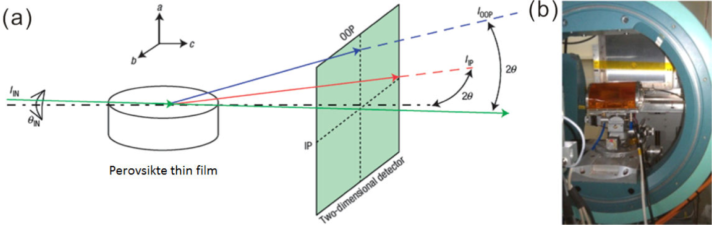
The 2D-GIXRD experimental set-up at SSRF
3. Results and Discussion
In order to get direct information about how the doping of CH3SH could affect the optical absorption properties and optical band gap of perovskite films, UV absorption spectroscopy was performed using a varying amount of CH3SH doped into CH3NH2PbI3 from 0.5% to 5%. As summarized in Figure 3, the absorption peak at the wavelength of around 750 nm for the conventional CH3NH2PbI3 perovskite film was recognized immediately at first glance [3,4]. Besides, another absorption characteristic at around 640 nm can also be identified clearly for the 1% doping of CH3SH, while more or less doped perovskite films exhibit very weak features around this wavelength. From these comparisons, it can be concluded that the doping of CH3SH into typical perovskite films indeed served as the tuning of the band gap of hybrid metal halide structures, and that the 1% doping of CH3SH seemed to be the optimized amount, which was also evidenced by the power convention efficiency measurements in the following section. Therefore, we will choose 1% doped CH3NH2PbI3 as the candidate for further exploration.
Various characterization techniques based on synchrotron radiation light have become powerful tools for materials science and nanoscience, owing to its high flux, high resolution and extreme quasi-monochromaticity. For example, synchrotron based X-ray diffraction can be used to investigate the structure and phase transition during diverse reactions or external treatments, owing to its outstanding ability of fast measurement. As realized, crystallographic data obtained from one-dimensional powder X-ray diffraction provide only limited structural information, in particular for the highly oriented perovskite thin films [28]. To this extent, the 2D GIXRD set-up at beamline BL14B in the SSRF opens a new door to the characterization of planar perovskite structures with the two-dimensional detection capability to probe the crystallographic orientations, as already illustrated in Figure 2.

UV absorption spectra of varying amounts of CH3SH doped perovskite films
Figure 4 shows the 2D GIXRD profiles of crystalline perovskite thin films as prepared with CH3NH3PbI3, and 1% doped CH3NH3PbI3 on flat ITO substrate as prepared following the recipe described above. It is easily seen from Figures 4a and 4b that a mixture of scattered secondary spots and rings coexist, which indicates that the crystalline domains are highly oriented in the in-plane direction [28]. Specifically, the 2D XRD patterns for CH3NH3PbI3 perovskite are highly ordered and uniformly distributed, with the scattering peak clearly showing at q=10 nm−1, which can be assigned to the (110) plane of CH3NH3PbI3 perovskite structure [2,8]. Moreover, distinct 2D XRD patterns present other q values, which are also manifest in the formation of high quality perovskite structure in our study; for example, the ring at q=20 nm−1 corresponding to the (220) plane and the ring at q≈25 nm−1 corresponding to the (310) plane [28]. Interestingly, visible changes were found when 1% CH3SH2 was doped into the CH3NH3PbI3 perovskite thin film, as seen in Figure 4b. While the pristine perovskite structure was surprisingly preserved, additional diffraction spots were resolved as well around the original (220) or (310) scattering rings. The emergence of new scattered spots herein can only be attributed to the introduction of CH3SH organic, since no other treatments or dopants were utilized. Surprisingly, the CH3SH dopant not only broke the original perovskite film, but also led to a new crystallike structure [29]. The originality of these new scattered spots may be related to the fact that the CH3SH dopant is distributed on top of the original perovskite nanostructures, while nanocrystalline was also formed by the template effect from perovskite substrate. Such a hypothesis is also confirmed by SEM measurements in the following section. In the end, it is worth pointing out that, although distinct peaks were observed, which enable us to determine the predominant sample structure in real time, the broad GIXRD scattering rings do not allow for precise structural assignments. The broadening (around 0.8 nm−1) of scattered rings may be related to the nanocrystalline structure or porous microstructure [28]
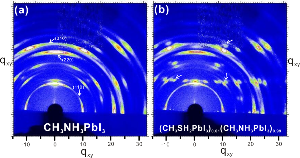
2D GI-XRD profiles of CH3NH3PbI3 (panel a) and 1% doped perovskite films with CH3SH (panel b) on planar substrate. It can be recognized that new scattered spots were introduced after doping (marked with white arrows), which is related to the doping of CH3SH organic. All the patterns are shown in q space.
Meanwhile, SEM measurements were also conducted in order to explore the morphology and structural differences between the original and doped CH3NH3PbI3 films. The planar and cross-sectional view are both depicted in Figure 5, with visible changes in film morphology and microstructures found within the SEM measurements. At a first glance, porous morphology and porous nanostructures can be identified from both perovskite films. Detailed analysis with zoom-in view (the inset in panel a) shows that the hole of porous nanostructure has an average size around 300 nm, which is probably the origin of the broadening of the scattered rings in Figure 4. Interestingly, the porous nanostructures are connected in some areas by the CH3SH organic chains, with the average length more than 500 nm (panel b), while the perovskite film gets much denser. As a result, the size of the pore was reduced considerably, such that it can be concluded that the filling factor was increased to some extent by the doping. The schematic illustration of a fabricated solar cell is shown in Figure 5c, and the cross-sectional view is presented in Figure 5d. The thickness of each individual layer was measured as follows: ITO, 150nm; PEDOT: PSS, 30 nm; Perovskite layer, 180nm; PCBM, 40 nm; ZnO, 120nm; Al electrode: 150 nm.

SEM micrographs of perovskite crystallization in thin films: (a) and (b) in-plane view for CH3NH3PbI3 and CH3SH doped perovskite film respectively, (c) the schematic structure of perovskite solar cell, and (d) the corresponding cross-sectional view
Since the UV absorption spectrum indicates the tuning of the band gap of perovskite film by CH3SH organic and the optimized doping around 1%, with the perovskite structures clearly resolved by the 2D GIXRD measurements for the mixture of 1% CH3SH and CH3NH3PbI3, one may spontaneously predict that the performance of the perovskite solar cell fabricated from the CH3SH doped CH3NH3PbI3 film should be enhanced to some extent. Therefore, a series of perovskite solar cells with different CH3SH doping from 0.5% up to 5% was fabricated and tested. For each certain doping, 10 devices were made and measured. In the end, statistic averaged results were adopted to ensure the reliability. Figure 6 presents the values of the short-circuit current density (Jsc), open-circuit voltage (Voc) and fill factor (FF) of differently doped perovskite solar cells. The increase in the average power convention efficiency from 6.9% for CH3NH3PbI3 to 7.9% for 0.5% doped perovskite and 9.4% for 1% doped CH3NH3PbI3 is encouraging, most probably due to the higher current density and fill factor [2, 6, 11, 26] compared to the original one. As evidenced by the XRD and SEM results, the increase in current density and fill factor can be attributed to the enhanced compact structure of perovskite film after certain doping of CH3SH; for example, the porous microstructure was covered or filled with CH3SH organic, while the size of the pore was reduced. As is generally the case, the structure of a certain interface plays a key role in the transport property of corresponding material (for example, the mobility of charge carriers, electrons or holes). As also pointed out by Wiesner et al. [28], it is believed that the enhanced perovskite structure with a complete pore network may facilitate the photo-generated electron generation and collection, enabling more uniform charge transport, which ultimately contributes to improvements in device performance. However, when the doping is more than necessary (it is proved to be 1% in our study), decline of the performance of solar cells was discovered, as in the case of 2% and 5% doped perovskite solar cell with CH3SH. The degrading of PCE at a higher doping concentration could be related to the breakage of the perovskite structure when too much CH3SH occupied the perovskite interface [18, 31]. To this extent, we can conclude that 1% doping of CH3SH is the optimal amount for the improvement in perovskite solar cells' performance in our study. Last but not least, as discovered in our measurement, there is a negligible J–V hysteresis in typical J-V curves. Similar behaviour has also been reported by Yang et al. [30] when using PCBM (PEDOT: PSS/PCBM interface combinations) as the top electron transport layers. While hysteresis is still a largely controversial issue in perovskite solar cells, more and more results have recently proposed that hysteresis originates from ion motion within the perovskite layer [32].

Current density/voltage curves of average performance of as-prepared CH3NH3PbI3 and varying amounts of CH3SH doped CH3NH3PbI3 perovskite solar cells
4. Conclusion
We have thoroughly investigated the doping effect of CH3SH organic on the structure and related performance of CH3NH3PbI3 perovskite solar cells, via in situ synchrotron-based GIXRD, together with SEM. In situ GIXRD investigations clearly illustrated the transformation of perovskite structures induced by the organic, which subsequently led to the enhancement of the power conversion efficiency of fabricated solar cells. With a series of doping of CH3SH at varying amounts, we found the optimized doping amount to be 1%. In the end, the possible explanation of the performance enhancement was proposed from the comparison of film morphology and nanostructure. Our study may ultimately present itself as an attractive strategy for the fabrication of high performance perovskite solar cells.
Footnotes
5. Acknowledgements
Fruitful discussions with Prof. Dr. Han Huang, Prof. Dr. Yunhao Lu and Dr. Zhenhua Chen are greatly acknowledged. Thanks to the SSRF for offering beamtime at BL14B beamline. This project was financially supported by the National Natural Science Foundation of China, under projects U1232112 and 91545101, the Hundred Talents Programme of the Chinese Academy of Sciences, SOE, and the Shanghai Pujiang Programme, under project No. 15PJ1410100.