
Abstract
The raising demand for efficient and stable energy sources for indoor applications demands the development of high‐performance photovoltaic (PV) materials. This study examines the potential of the all‐inorganic CsPbIBr2 perovskite material as a promising photoactive absorber for perovskite solar cells (PSCs) designed for indoor applications. CsPbIBr2 exhibits a favorable balance between optical bandgap and phase stability among other all‐inorganic constituents. Additionally, CsPbIBr2 possesses a wide direct bandgap of 2.05 eV, elevated absorption coefficient, and high carrier mobilities, compelling it well‐suited for harnessing photon energy from indoor lighting sources. Our research commenced with an experimental CsPbIBr2‐based solar cell demonstrating a power conversion efficiency (PCE) of 11.01% under 1‐sun illumination, with an initial device structure of ITO/ZnO/CsPbIBr2/Spiro‐OMeTAD/Au. We initiated our investigation using SCAPS‐1D to validate the simulation approach, replicating experimental current–voltage characteristics and identifying a critical limitation in the single electron transport layer (ETL) design: suboptimal band alignment. This insight drives a comprehensive optimization strategy relating a double ETL configuration, exploring optimal transport layer materials, followed by analyzing absorber layer thickness and defect concentrations. Through this methodical approach, we progressively enhanced the cell’s performance, achieving a remarkable 21.85% a PCE under 200 lux, and a 2900 K indoor LED illumination. The simulation results provided in this study reveal the prospective of CsPbIBr2 PSCs as a promising candidate for indoor PV applications.
1. Introduction
Photovoltaic technology has appeared as a pronounced solution to the growing energy demands, presenting a renewable alternative to traditional sources [1]. In recent decades, the PV market has been dominated by Si‐based PV cells, accounting for over 90% of the global market share [2]. However, the need for higher power efficiencies has urged researchers to explore new device designs and material compositions, paving the way for the development of thin‐film solar cell technologies (TFSCs) [3–7]. TFSCs, such as those based on CdTe [8], antimony‐based chalcogenide [9], and copper‐based chalcogenides [10], have gained substantial attention owing to their potential advantages. These technologies offer the promise of lower material consumption and lightweight properties, as well as the ability to be deposited on flexible substrates, enabling integration possibilities. In this context, perovskite solar cells have rapidly evolved over the past decade, emerging as a highly efficient and cost‐effective thin‐film technology. Notably, lead‐based perovskite solar cells dominate the field due to their exceptional PCEs; however, significant progress is also being made in the development of lead‐free perovskite materials. Despite the progress in lead‐free materials, lead‐based PSCs remain superior in terms of efficiency, and ongoing research is focused on minimizing their environmental impact, such as through improved encapsulation and recycling techniques.
Organic–inorganic hybrid PSCs have surpassed 25% efficiency due to their superb absorption coefficients and low exciton binding energies. However, a significant drawback is their instability under thermal, moisture, and photo stresses [11, 12]. All‐inorganic perovskites have several advantages over their hybrid organic–inorganic counterparts, including superior thermal stability, enhanced moisture resistance, and elimination of volatile organic components that typically degrade under operational conditions. For the complete substitution of organic components in photoactive materials, numerous all‐inorganic photoactive materials, such as CsPbBr3, CsPbI2Br, and CsPbIBr2, have been widely researched [13–15]. Notably, Cs‐based PSCs have gained significant attention due to their exceptional charge carrier mobilities and high thermal stability [16]. These materials are capable of maintaining a stable phase even at temperatures exceeding 400°C, making them a promising strategy to mitigate thermal decomposition and phase transitions besides bias‐induced ion migration [14]. Among them, CsPbIBr2 offers an optimal balance between light harvesting capability and phase stability. Its bandgap of approximately 2.05 eV, coupled with remarkable thermal stability up to 460°C, positions CsPbIBr2 as a promising solution to PSC technology [17].
Recent progress in material synthesis and diverse device engineering methods has resulted in substantial advances in CsPbIBr2 cell performance. In 2016, Ma et al. achieved a PCE of 4.7% for CsPbIBr2‐based PSCs utilizing a dual‐source thermal evaporation method [18]. Further, Zhu et al. used a simple intermolecular exchange strategy. This technique produces high‐quality films with desirable large grain sizes and high crystallinity. When used in carbon‐based all‐inorganic planar PSCs, these films achieve an optimized efficiency of 9.16% [19]. Wang et al. enhanced CsPbIBr2 film performance by adding sulfamic acid sodium salt, creating an internal electric field that boosted electron transport and injection. This modification resulted in an improved PCE of 10.57% [20]. In 2022, Huang et al. implemented a simple dynamic vacuum‐assisted‐low‐temperature process, which has resulted in an optimized morphology and efficient charge dynamics of CsPbIBr2 cells, which contributes to a high JSC (11.34 mA/cm2) and an FF of 75.31%, coupled with a PCE of 11.01% and a VOC of 11.289 V [21]. Furthermore, Yu et al. boasted a record efficiency of 12.8% by using a triple‐component precursor system. Their approach produced high‐quality CsPbIBr2 films with improved crystallinity, larger grains, and fewer defects attaining an improved PCE, along with an enhanced JSC [22].
The prospective of CsPbIBr2 solar cells extends beyond outdoor applications, as they can also be tailored for indoor applications. Remarkably, solar cells designed for indoor environments must be capable of efficiently harnessing the narrower spectrum and lower light intensities typical of indoor lighting conditions [23, 24]. The wide bandgap of CsPbIBr2 makes it a promising material for indoor applications. While numerous photoactive materials, including Si, a‐Si, organic, sensitized dyes, and perovskites, have been previously investigated for indoor use [25–30], the potential of CsPbIBr2 in this context has not been extensively explored. Notably, the maximum theoretical efficiency for a 2.05 eV bandgap solar cell under AM1.5G illumination is estimated to be around 22% and around 45% for a white LED source [31]. Thus, this potential makes CsPbIBr2 a promising candidate as a target perovskite material for indoor photovoltaic applications.
Inspired from the previous discussion, our aim in this work is to investigate the potential of CsPbIBr2 for in use in indoor applications. This simulation‐based study presents a comprehensive investigation into the indoor application of CsPbIBr2 PSCs, specifically under the influence of LED illumination with varying color temperatures and light intensities. Our study focuses on an experimentally fabricated CsPbIBr2‐based cell with a PCE of 11.01% under 1‐sun illumination, utilizing a device structure of ITO/ZnO/CsPbIBr2/Spiro‐OMeTAD/Au [21]. To validate our modeling approach, we have replicated the experimental current–voltage (J–V) characteristics and other metrics reported for the previously fabricated cell by means of a SCAPS‐1D device simulator. This calibration step proves the credibility of our simulations and paves the way for further optimization and design exploration. Recognizing the limitations of single‐layer electron transport layer (ETL) designs in achieving optimal band alignment of the absorber/ETL and ETL/front contact interfaces, we propose the implementation of a double ETL structure, with one layer tailored to the interface with the absorber addressing the conduction band offset (CBO) issue and the other addressing the alignment with the front contact. This technique presents a favorable solution to improve the charge transport and collection within the CsPbIBr2‐based solar cell, thereby enhancing the overall cell performance and suitability for indoor PV applications.
2. Materials and Methodologies
This section provides a detailed overview of the materials, device architecture, and simulation approaches employed in this study. The first subsection describes the structure of the PSC modeled in this study, based on an experimental configuration reported in prior research. Cell architecture comprises layers including ITO, ZnO, CsPbIBr2, Spiro‐OMeTAD, and Au. The second subsection highlights the simulation approach, where the simulation framework is built around the SCAPS‐1D software. This subsection outlines the equations and physical principles underlying the simulations. The calibration of the CsPbIBr2 PSC is presented in the third subsection. Besides, a comparison between simulations and experimental results is demonstrated to ensure simulation reliability.
2.1. Solar Cell Configuration
The CsPbIBr2‐based cell employed in our simulations is based on an experimental cell, as mentioned before [21]. The structure of the cell follows the sequence of ITO (front contact)/ZnO (ETL)/CsPbIBr2 (absorber)/Spiro‐OMeTAD (HTL)/Au (metal back contact), as presented in Figure 1(a). Figure 1(b) illustrates the energy diagram of the utilized materials. This n+–p–p+ heterostructure incorporates a highly n‐doped ETL to enhance electron conductivity and facilitate efficient electron extraction, a low‐doped p‐type light‐absorbing layer, and a highly p‐doped HTL to promote hole conductivity and enable effective hole collection. The CsPbIBr2 cell fabrication included spin‐coating CsPbIBr2 precursor solution onto a ZnO film of an estimated thickness to be 50 nm. The as‐prepared film was briefly annealed at 40°C and then subjected to a vacuum‐assisted low‐temperature process. This vacuum‐assisted method enabled optimized CsPbIBr2 film formation at lower temperatures. The produced CsPbIBr2 layer has a thickness of 315 nm. More about fabrication processes can be found in [32].

(a) Basic CsPbIBr2‐based cell structure and (b) energy level profile for the different cell layers.
(b)

The experimental results indicated that the valence band maximum (VBM) and conduction band minimum (CBM) of the CsPbIBr2 layer are −5.36 and −3.31 eV, respectively. Further, the estimated carrier diffusion length is 210 nm, while the carrier mobility in the absorber layer is around 10 cm2/V·s. The work functions are set at 4.4 and 5.1 eV for the front and rear contacts, respectively, where the ITO front contact was modeled by including a filter file (including transmission spectrum of the ITO) incorporated in a SCAPS simulator and adjusted to reproduce the measured EQE spectrum [33]. In addition, a series resistance of 3.8 Ω·cm2 was added to fit the experimental J–V data. Table 1 lists the main material factors needed for the device simulator. In addition, the bulk and interfacial defect parameters are shown in Table 2. The absorber defect concentration used was the same value as the reported fabricated cell, while the other values were adjusted as fitting parameters.
Input physical parameters of the materials employed in the device simulator.
Note: µ n and µ p : electron and hole mobilities, respectively; N V and N C : effective density of states; N D and N A : donor and acceptor doping concentrations, respectively; ε r : relative permittivity.
Defect parameters of the absorber and at the interfaces applied in device simulation.
2.2. Simulation Approach
Simulation shows a critical role in PV technology as it facilitates the design and development of solar cells by allowing researchers to model and predict cell behavior without the need for extensive physical prototyping. One such simulation tool is SCAPS‐1D [35], which allows users to test the behavior of solar cells under various operational conditions, including varying illumination intensity and applied voltage [36–38]. SCAPS‐1D uses fundamental semiconductor equations to model solar cell behavior. These equations contain the Poisson equation, continuity equations, and current density equations. The software solves these coupled differential equations numerically to simulate the electrical characteristics of the solar cell. SCAPS‐1D simulator can produce a wide range of results, including J–V and C–V characteristics, and external quantum efficiency (EQE) spectra, providing valuable insights into cell performance and enabling optimization of solar cell devices.
In SCAPS‐1D, the one‐dimensional Poisson’s equation along with continuity equations are solved self‐consistently through an iterative process until convergence is achieved. Poisson’s equation is given in equation (1), while the continuity equations are provided in equations (2) and (3)

The bulk Shockley–Read–Hall (SRH) recombination rate is specified by equation (4) where τ
n
and τ
p
are bulk lifetimes,
Interface SRH recombination is given by equation (5) with S
n
and S
p
representing interface recombination velocities,
Lastly, transport equations based on the drift‐diffusion modeling technique, which are used to estimate electron and hole current densities, are given in equations (6) and (7),

2.3. Calibration of the CsPbIBr2 Solar Cell
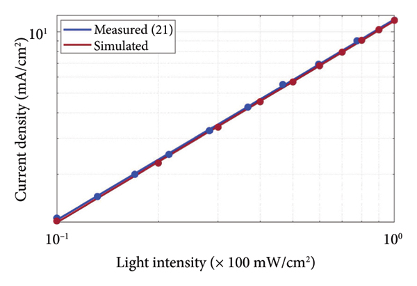
To ensure the accuracy of the simulation model, this subsection details the calibration process by comparing SCAPS‐simulated results with measured records. The precision of these simulations is intrinsically linked to the precision of the input factors and material physical and technological properties used in the model. To validate our simulation, the J–V (Figure 2(a)), EQE (Figure 2(b)) curves, and dependence of light intensity (I) dependence of both JSC (Figure 2(c)) and VOC (Figure 2(d)) were plotted under AM1.5G irradiation, derived from both SCAPS‐1D simulations and experimental measurements as reported in [39]. This calibration step guarantees that the simulation model precisely replicates the behavior of the fabricated CsPbIBr2 PSC. Additionally, we conducted a detailed comparative analysis, presented in Table 3, which contrasts key metrics between measured and simulated findings. The close alignment observed between these two datasets not only underscores the accuracy of our simulation model but also affirms its predictive capabilities, providing a solid foundation for further exploration and optimization of CsPbIBr2‐based PSCs.

Experimental and simulated CsPbIBr2 cells: (a) J–V curves, (b) EQE, and the dependence on light intensity of (c) JSC and (d) VOC.
(b)

(c)
(d)

PV metrics for experimental and simulated CsPbIBr2 cells.
3. Results and Discussions
This section presents a comprehensive analysis of our optimization strategies for CsPbIBr2‐based PSCs designed under LED illumination. We begin by assessing the performance of the initial baseline cell under LED conditions in Section 3.1. The implementation of a double ETL design is examined in Section 3.2, where we address critical interface issues including CBO and band alignment to enhance electron transport efficiency. Section 3.3 investigates the relationship between the absorber layer thickness and defect concentration. All simulations were conducted under the 200 lux and 2900 K LED illumination conditions [38, 39]. These specific conditions were chosen to closely mimic typical indoor lighting environments. Section 3.4 integrates these optimization approaches to evaluate the cumulative performance improvements where we expanded our analysis to include additional color temperatures (5300 and 7500 K), comparing our fully optimized design with the initial cell configuration through detailed analysis of J–V characteristics and key performance metrics. Section 3.5 examines the impact of series and shunt resistances on device performance. Finally, Section 3.6 investigates the role of charge carrier mobilities in both initial and optimized cell configurations.
3.1. Initial Cell Performance Under Indoor LED Illumination
The performance of the CsPbIBr2‐based PSC under indoor lighting conditions is presented in Figure 3. When tested under LED illumination (with an intensity of 200 lux and a color temperature of 2900 K), the cell exhibited remarkable performance metrics with a VOC of 1.114 V, a JSC of 9.09 μA/cm2, and an FF of 82.73%. These parameters collectively resulted in a PCE of 14.47%. The satisfactory performance under low‐light intensity can be ascribed to the wide bandgap (2.05 eV) of the CsPbIBr2 absorber, which is particularly well‐suited for harvesting the narrow spectrum of LED illumination. These characteristics position CsPbIBr2‐based PSCs as favorable candidates for indoor PV applications.
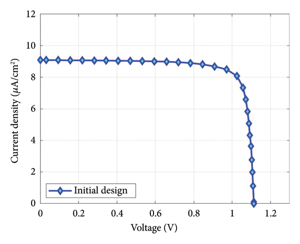
J–V curve of the calibrated cell design under LED illumination (200 lux and 2900 K).
3.2. Double ETL Design
To create high‐performance CsPbIBr2‐based solar cells for indoor use, the ETL materials need definite characteristics. An important factor to be looked at is the CBO at the absorber/ETL interface (see equation (8)). The ZnO layer used as an ETL in the initial cell design has a negative CBO of −0.69 eV that needs improvement as a previous study showed that the ideal CBO for a PSC is between 0 and 0.3 eV [38]
A crucial factor for the design is also the barrier height, faced by the majority carriers, between the ETL and front ITO contact. To address these issues, a double ETL design has been researched. This approach utilizes two distinct materials instead of a single ETL to address the limitations of traditional single ETL designs. One layer is specifically designed to interface with the absorber, tackling the CBO issue, while the other layer focuses on aligning with the front contact to amend charge transport and collection. This dual‐layer strategy enhances the performance of solar cells overall. Numerous experimental investigations have been performed focusing on double ETL structures to increase the efficiency of PV cells [40–45].
To find the optimum choice for a double ETL design, Figure 4 shows the PCE for different electron affinity values for both ETL layers. The simulations were performed under LED illumination (200 lux and 2900 K). We obtained a PCE of 16.81%, with an ETL featuring an electron affinity of 3.3 eV on the absorber side (resulting in a CBO value of +0.01 eV) and an ETL with an electron affinity of 4.0 eV on the ITO contact side, which provides better band alignment. Significant PCE drops are observed when electron affinities deviate from the optimal range. The figure underscores the critical importance of carefully selecting ETL materials to optimize energy band structures and minimize interface recombination.

Dependence of PCE on electron affinities of the double ETL layers (contact side ETL and absorber side ETL).
The band alignment analysis shown in Figure 5 reveals distinct interface characteristics that significantly influence the cell’s performance, particularly at the ETL/absorber heterojunction, while maintaining a fixed barrier with front contact. Figure 5(a) shows a small spike‐like band at the absorber’s side where a CBO of +0.01 eV is achieved through the double ETL structure. This minor spike‐like offset plays a crucial role in controlling charge carrier dynamics. The device exhibits enhanced performance with an increased PCE of up to 16.81% (compared to 14.47% for the single ETL design). This improvement can be credited to the favorable energy barrier formation that limits interface recombination while still allowing efficient electron transport. Thus, the CBO dominates the performance by optimizing electron transport across the junction while simultaneously mitigating SRH recombination at the interface. The PCE would be further enhanced; however, a high energy barrier exists between the two ETLs that limits this improvement.

Band alignment analysis: (a) CBO = +0.01 eV, (b) CBO = −0.39 eV, (c) CBO = −0.59 eV.
(b)

(c)

In contrast, the subsequent cliff‐like band alignments, plotted in Figure 5(b), demonstrate declining characteristics. The negative CBO (−0.39 eV), while not impeding electron flow, creates conditions where interface recombination becomes the dominant loss mechanism, as evidenced by the reduced activation energy below the absorber’s bandgap with a PCE of 16.27%. This interface‐dominated recombination arises from the inadequate energy barrier at the ETL/absorber interface, which results in increased carrier recombination through interface states. However, the efficiency loss is not so large compared to the previous case because of the reduced barrier between the two ETLs. Although Figure 5(c) shows the case with the lowest barrier between the two ETLs, the cliff‐like band alignment at the absorber/ETL side also demonstrates deteriorating characteristics. In this case, the CBO is more negative (−0.59 eV), resulting in increasing interface recombination losses and a reduced PCE of 15.82%.
This comprehensive analysis underscores the critical importance of precise band alignment engineering in achieving high‐performance TFSCs. The barrier height between the two ETLs significantly influences charge transport efficiency and overall device performance. A lower barrier results in a smoother electron flow between the ETL layers, reducing transport resistance and improving current collection. However, this must be balanced against the interface conditions at the absorber/ETL junction, where the CBO plays a more dominant role in determining recombination losses. The carefully engineered double ETL structure with minimal positive CBO demonstrates significant potential for future device optimization. In this regard, we provide a design that utilizes ZnO as the ETL layer at the contact side and In2O3 at the absorber side and the device structure becomes ITO/ZnO/In2O3/CsPbIBr2/Spiro‐OMeTAD/Au. These two materials were chosen according to their suitable band offsets with CsPbIBr2, as can be depicted from their physical properties listed in Table 4.
Input parameters of the ETL materials applied in double ETL simulations.
In Figure 6, we present a comparison between the J–V curves of our proposed double ETL design and the initial cell design, which was mentioned in Section 3.1. When examining JSC, one can observe no significant differences between the two designs. However, VOC shows a substantial increase from 1.114 to 1.295 V. This can be directly attributed to the implementation of the double ETL structure. Despite this improvement in voltage, the FF experienced a minor decrease from 82.73% to 82.57%. Most importantly, these changes culminated in a significant enhancement of the PCE, which increased from 14.47% to 16.81%. All simulations were conducted under LED conditions of 200 lux and 2900 K.

J–V curve for both initial cell design and double ETL cell design under LED illumination (200 lux and 2900 K).
3.3. Absorber Thickness and Defects
This subsection looks at the intricate relationship between absorber layer features (thickness and defects) and the efficiency of CsPbIBr2 PSCs. Figure 7 shows how the absorber layer thickness affects performance across different defect levels. The concentration of defects within the CsPbIBr2 layer greatly impacts how well PSCs perform. More defects can lead to increased carrier recombination, which negatively affects the VOC of the cell. For instance, examining the performance metrics of a perovskite layer with a defect concentration of 1015 cm−3 reveals that increasing the thickness below a certain threshold enhances the PCE of the solar cell due to reduced recombination. The optimal thickness for this specific defect concentration is approximately 600 nm, having a PCE of 17.71%. Beyond this thickness, the absorber layer becomes too thick, leading to increased trapping of charge carriers, making it more difficult for the charge carriers to reach the electrodes. This, in turn, reduces the charge collection efficiency and lowers the overall PCE. The threshold absorber thickness for every defect concentration is related to the diffusion length, where at a defect concentration of 1016 cm−3, the diffusion length is 250 nm leading to a drastic reduction in PCE when the absorber thickness exceeds this value. In contrast, at lower defect concentrations (N t = 1015 cm−3, diffusion length ∼750 nm; N t = 1014 cm−3, diffusion length ∼2500 nm), the longer diffusion lengths allow for better carrier collection even at greater thicknesses, resulting in more gradual PCE variations.

PCE for different absorber thicknesses across different defect levels for the initial cell design under LED illumination (200 lux and 2900 K).
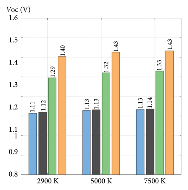
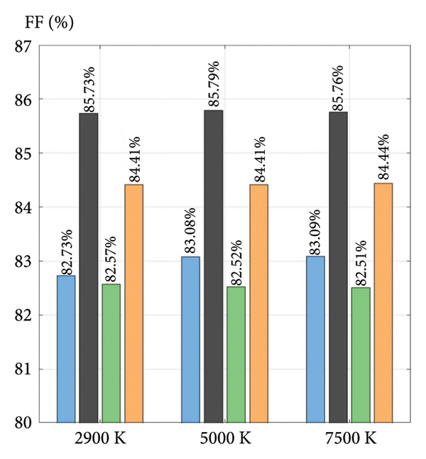
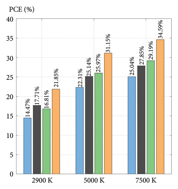
3.4. Optimized CsPbIBr2 Solar Cells Under Different Color Temperatures and Light Intensities
A systematic investigation was conducted to evaluate the cumulative impact of our optimization strategies compared to the initial cell design. Our analysis encompassed the initial CsPbIBr2 cell response to LED color temperatures of 2900, 5300, and 7500 K. Figures 8(a), 8(b), 8(c) present J–V characteristics at different LED conditions comparing four configurations: the initial cell; cell with an optimized thickness of 600 nm cell with a reduced defect concentration of 1015 cm−3; cell with double ETL structure without other optimizations; and our fully optimized design incorporating both double ETL and enhanced parameters (600 nm thickness, 1015 cm−3 defect concentration). Figure 8(a) illustrates the J–V characteristics under LED illumination 2900 K, while Figures 8(b), 8(c) illustrate the J–V characteristics under LED illumination 5300 and 7500 K, respectively.

J–V curves at different optimization stages under LED illumination: (a) 2900 K, (b) 5300 K, and (c) 7500 K.
(b)

(c)

The initial cell design demonstrated baseline performance with the lowest current density and open‐circuit voltage. As the thickness was optimized to 600 nm with a defect concentration reduced to 1015 cm−3, an improved JSC with a slight increase in the overall performance was observed, aligning with findings detailed in Section 3.3. The double ETL architecture demonstrated substantial improvements in VOC, as discussed in Section 3.2. The fully optimized design, which included a double ETL configuration, thickness modifications, and defect reduction, showed the highest performance across all color temperatures with significant improvements in voltage and current density.
Statistical analyses of key performance parameters (JSC, VOC, FF, PCE) are presented in Figures 9(a), 9(b), 9(c), 9(d). JSC exhibited a positive correlation with LED color temperature elevation reaching its highest point at 7500 K, with optimization strategies progressively improving current collection (Figure 9(a)). As can be deduced from Figure 9(c), VOC remained relatively constant across diverse color temperatures, experiencing a slight increase with optimization, particularly in the double ETL design. The FF maintained consistent performance around 82%–83% across different color temperatures (Figure 9(c)). The PCE exhibited improvement (Figure 9(d)) with a positive correlation, with temperature reaching peak performance at 7500 K. The fully optimized design exhibited a substantial PCE increase compared to the initial design.

Comparison between performance metrics at different optimization stages under LED illumination: (a) JSC, (b) VOC, (c) FF, and (d) PCE.
(b)
(c)
(d)
In Figure 10, we studied the output power characteristics of our proposed fully optimized cell under different LED illumination conditions. The graph plots the power output (μW/cm2) against power input (μW/cm2) on logarithmic scales, with variations taken from 200 lux up to approximately 12,000 lux, assuming a cell area of 1 cm2 that could be increased by connecting sub‐cells in a module. The results show that higher color temperature LEDs (7500 K) consistently produce greater power output compared to lower color temperatures (2900 K). Importantly, the figure includes horizontal reference lines indicating the typical power consumption of various low‐power electronic devices, including wireless sensors (∼1 mW), acoustic sensors (∼100 μW), RFID tags (∼10 μW), calculators (∼1 μW), and real‐time clocks (∼100 nW) [47]. The power output levels that could be achieved by the proposed wide bandgap CsPbIBr2 PSC confirm its practical viability for indoor energy harvesting applications, which support IoT devices that operate in the sub‐milliwatt range typical of indoor lighting conditions.
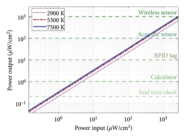
Power output characteristics of the fully optimized cell under different LED color temperatures with power consumption ranges of various low‐power electronic devices (assuming a cell area of 1 cm2).
Next, Figure 11(a) shows the performance of the fully optimized cell versus the initial cell at all LED color temperatures investigated, where the fully optimized cell always shows improved performance metrics consistently at any color temperature. The EQE analysis (Figure 11(b)) shows enhanced spectral response in the fully optimized cell, which emphasizes the improved light harvesting and charge collection efficiency. Table 5 provides a comparison of the PCE of all design variants at different LED color temperatures, including design parameters of each optimization step. These findings indicate that combining double ETL architecture with optimized thickness and reduced defect concentration represents a promising direction for future research in PSC development. The enhanced performance parameters suggest potential applications in indoor PV systems.

Performance comparison between the fully optimized cell and the initial cell under LED illumination: (a) J–V curves and (b) EQE.
(b)

Comparison between PCE at different optimization stages under different LED color temperatures.
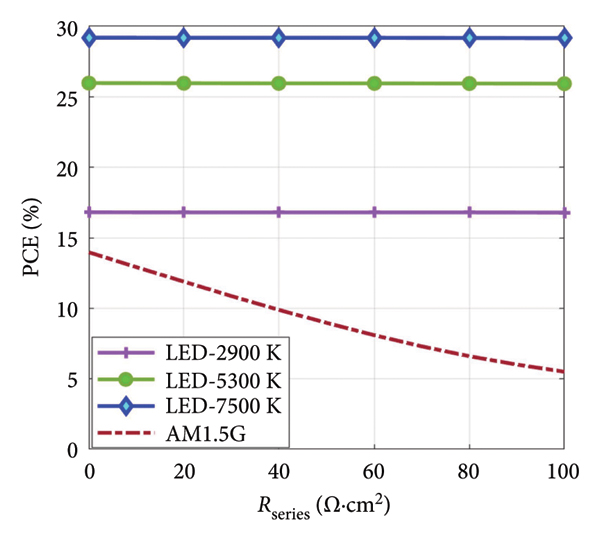
3.5. Impact of Series and Shunt Resistances
In this part, we investigate the influence of series and shunt resistances (Rseries and Rshunt) on the performance of our optimized CsPbIBr2 solar cells under indoor illumination conditions. Understanding these resistance effects is important for practical implementation of indoor photovoltaic systems. The analysis of Rseries and Rshunt effects on PCE reveals different behaviors under indoor versus outdoor illumination conditions. Figure 12(a) shows that Rseries has a minimal impact on device performance across all indoor LED conditions, where PCE remains stable at series resistance values up to 100 Ω·cm2, which can be explained by the low current densities. Under AM1.5G illumination, however, the device exhibits significantly higher sensitivity to series resistance, with PCE dropping from 13.97% to approximately 5.5% at 100 Ω·cm2, highlighting the critical importance of a minimum Rseries for outdoor applications.
PCE at AM1.5G and various LED color temperatures: (a) Rseries analysis and (b) Rshunt analysis.
(b)
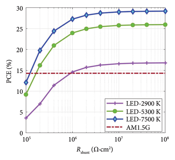
In contrast, Figure 12(b) shows that Rshunt has a pronounced influence on PCE, particularly for values below 106 Ω·cm2 across all color temperatures. The simulation results show that the shunt resistance represents a critical parameter to achieve high indoor PV performance, which could be enhanced through optimizing the quality of the absorber layer, interface defect densities, and film morphology to avoid parasitic current paths. On the other hand, under AM1.5G illumination, the device does not show any significant variation in its PCE. The observed behavior of Rseries and Rshunt on device performance aligns with fundamental PV principles reported in the literature [48].
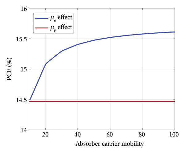
3.6. Impact of Charge Carrier Mobilities
The impact of carrier mobility variations on device performance under 2900 K LED illumination conditions is depicted in Figure 13. The absorber layer carrier mobility for both electrons and holes was varied from 10 to 100 cm2·V−1·s−1. In the initial unoptimized cell (Figure 13(a)), hole mobility variations have minimal impact on PCE, which remains constant at 14.47%, while electron mobility shows a more pronounced effect where PCE increases from 14.5% to 15.7%. In the fully optimized cell (Figure 13(b)), the roles reverse with hole mobility variations causing a slight improvement in PCE from 21.8% to 22.1%, while electron mobility effects become negligible. This behavior indicates that the comprehensive optimization process has improved band alignment and reduced interface recombination via the double ETL configuration and has effectively eliminated electron transport bottlenecks, making hole extraction the limiting factor.
Impact of charge carrier mobility on PCE at 2900 K and 200 lux conditions: (a) initial cell and (b) fully optimized cell.
(b)

4. Conclusions
This comprehensive study investigated the potential of CsPbIBr2 PSCs for indoor PV applications. After validating our simulation approach through comparison with experimental results, we systematically optimized the device architecture by implementing a double ETL configuration, fine‐tuning the absorber layer thickness, and reducing defect concentration. Using two different materials for ETL instead of just one resulted in higher performance. The ZnO layer at the contact side and the In2O3 layer at the absorber side fixed the energy level mismatch problems. Our band alignment analysis revealed that a minimal positive CBO of +0.01 eV creates optimal conditions for efficient electron transport while simultaneously reducing interface recombination.
The optimized double ETL configuration increased the VOC from 1.114 to 1.295 V while maintaining a high fill factor of 82.57%, resulting in a PCE improvement from 14.47% to 16.81% under 200 lux and 2900 K LED illumination. Further optimization of absorber thickness to 600 nm and reduction of defect concentration to 1015 cm−3 led to additional enhancements in JSC, boosting the overall PCE to 17.71% under the same illumination conditions. Our fully optimized CsPbIBr2 solar cell achieved a remarkable PCE of 21.85% under 200 lux and 2900 K LED illumination, with performance improvements evident across all tested color temperatures. The device maintained excellent performance with PCEs of 31.15% and 34.59% under 5300 and 7500 K LED illumination, respectively, demonstrating its versatility across various LED color temperatures. These values represent significant improvements over the initial cell design, which exhibited PCEs of 14.47%, 22.31%, and 25.04% under the same respective lighting conditions.
The thermal and moisture stability inherent to the all‐inorganic perovskite CsPbIBr2 material, coupled with the enhanced efficiency achieved through our optimization strategies, can position CsPbIBr2‐based PSCs as highly promising candidates for indoor energy harvesting solutions. The findings from this study provide valuable insights into future experimental work of efficient, stable, and cost‐effective indoor PV technologies. Future research could focus on enhancing long‐term performance under diverse environmental conditions through advanced passivation techniques. Additionally, improving the scalability of CsPbIBr2 production is critical for commercial viability, which could involve optimizing the synthesis processes to ensure high‐quality, large‐area films while maintaining the performance characteristics observed in smaller‐scale devices.
Data Availability Statement
The data that support the findings of this study are available from the corresponding author upon reasonable request.
Conflicts of Interest
The authors declare no conflicts of interest.
Author Contributions
Conceptualization, Mona El Sabbagh, Marwa S. Salem, Mohamed Okil, and Ahmed Shaker; funding acquisition, Mostafa Salah; investigation, Mostafa Hamed, Mohamed Okil, Mostafa Salah, and Ahmed Shaker; methodology, Mona El Sabbagh, Marwa S. Salem, Mohamed Okil, and Mostafa Salah; resources, Marwa S. Salem; software, Mostafa Hamed, Mona El Sabbagh, Mohamed Okil, and Ahmed Shaker; supervision, Mona El Sabbagh and Ahmed Shaker; validation, Mostafa Hamed, Mona El Sabbagh, Mostafa Salah, and Ahmed Shaker; visualization, Mona El Sabbagh, Marwa S. Salem, Mohamed Okil, and Mostafa Salah; writing–original draft, Mostafa Hamed, Marwa S. Salem, and Mohamed Okil; writing–review and editing, Mostafa Hamed, Mostafa Salah, and Ahmed Shaker.
Funding
The authors received no specific funding for this work.