
Abstract
Utilizing ABX3-based perovskites for solar cell applications has proven to be a sustainable choice, offering a suitable substitution for non-renewable energy sources. However, employing these types of solar cells is challenging due to the thousands of possible perovskite solar cells that can be formed. The present study focused on selecting a suitable perovskite solar cell structure among commonly considered organic-inorganic solar cell structures. This was achieved by classifying performance data from poor to good and screening the good data for further investigation. Following this selection, the optimization process was initiated to improve cell performance. This process was accomplished in several phases, including optimization of perovskite solar cell layer properties and working points. The results of perovskite layer optimization indicated that, with respect to recombination issues, choosing a cell with relatively high absorber thicknesses and low perovskite layer doping densities yields better performance. For working point optimization, simulation results suggested lower temperatures and series resistances, and higher shunt resistances. Results revealed that the CuSCN/TiO₂/FASnI₃ structure achieved the highest power conversion efficiency of 26.03%, with a short-circuit current density of 27.75 mA·cm⁻², an open-circuit voltage of 1.13 V, and a fill factor of 83.16%. The optimization process employed in this study led to a 1% efficiency improvement, raising the efficiency to 26% based on an optimized structure.

Introduction
Perovskite semiconductors possess some tremendous properties including their high dielectric constants, tunable band-gaps, and ferroelectric behavior that makes them ideal for photovoltaic applications. Regarding these features, and also their cost effectiveness, they can be a good substitiute to the traditional silicon solar cells.1,2 However, due to stability and environmental toxicity issues, they are not yet commercialized. 3 Perovskite solar cells (PSCs) operate based on a perovskite-based absorber layer that generates electrons and holes, leading to electricity generation. In the case of solar cell applications, the general formula of the perovskite layer is ABX3, where A, B, and X refer to a monovalent cation, divalent cation, and halide ions, respectively. 3 Hundreds of perovskite formulas can be formed due to the wide variety of these ions. In the early years of PSC research, methylammonium lead-based perovskites were commonly employed because of their significantly higher performance.3,4 However, employing these PSC structures caused hazardous environmental impacts and stability issues, 5 – 7 which motivated renewed interest in studying lead-free PSCs. 8
In addition to the perovskite absorber layer, other layers must be included in a PSC structure. They consist of charge-transporting and charge-collecting layers. Since two different charges (electrons and holes) are generated from the absorber, the additional layers include electron-transporting material (ETM), hole-transporting material (HTM), a metal electrode (anode), and a transparent glass electrode (cathode). In a PSC structure, the absorber, ETM, and HTM layers constitute the active layers of the cell. Thus, they are more critical than the electrodes, and most research innovations around PSCs focus on variations of the active layers. HTM and ETM layers can consist of various organic and inorganic materials. 3 Consequently, thousands of PSC structures can be formed.
As with all solar cell studies, PSC research can be carried out in both experimental and simulation phases. 9 Simulation provides useful insights into the parameters influencing solar cell performance and helps experimental work focus on targeted aspects. For instance, rapid optimization processes performed in solar cell simulation software can determine optimized layer thicknesses, guiding subsequent experimental efforts.
Inspired by previous simulation studies, the present research gives results in four phases. First, considering eight different methylammonium-based and formamidinuim-based absorbers, three different organic and inorganic HTMs, and three different ETMs (yielding 72 unique PSC structures), the photovoltaic parameters of each structure were reported, and optimal results were collected. In the next steps, based on the obtained optimal PSC structures, the layer properties and working points of simulation were optimized. Finally, the overall I-V results are reported in tabular form and as I-V curves. This work emphasizes on the batch calculations of the selected software for PSCs’ simulation. To the best of our knowledge, no other study represents the importance of batch study by detail. The batch study of software helps rapid selection of structures. Therefore, finding a proper PSC structure for the experimental and fabrication phase will be easier.
Materials and methods
To achieve the objectives of this study, we performed numerical simulations of perovskite solar cells using the SCAPS-1D software. 10 The software simultaneously solved the electron and hole continuity equations along with Poisson’s equation to compute device performance parameters, including current–voltage (I–V) characteristics, fill factor (FF), power conversion efficiency (PCE), open-circuit voltage (VOC), short-circuit current density (JSC), quantum efficiency (QE), and generation–recombination profiles. 11
All simulations were conducted under standard test conditions: a temperature of 300 K and AM1.5G illumination with an incident power of 100 mW·cm⁻². The key material properties required by SCAPS, such as thickness, doping concentration, electron and hole mobilities, permittivity, and defect densities, were defined for each layer and are summarized in Tables 1–4. Using these inputs, we systematically varied absorber layer thickness, doping densities, transport layer combinations, and resistive/temperature conditions to investigate their effects on the photovoltaic performance of the simulated devices.
Electrical properties of methylammonium-based absorbers utilized in the study.

Electrical properties of formamidinuim-based absorbers utilized in the study.


In the case of resistances, it is better to have lower series resistance and higher shunt resistances because they represent the resistance to charge generation and recombination, respectively. 10 The reflection parameter should be set according to the experimental fabrication conditions. As can be seen from Tables 1–4, different organic and inorganic ions and materials were considered for each layer to investigate their performance. For perovskite materials in PSCs, the MA+, FA+, Cs+, Pb2+, Sn2+, I-, Br-, and Cl- ions are the most commonly employed and high-efficiency candidates. Therefore, using the literature data in Tables 1 and 2, eight different absorbers were considered to investigate the performance of each of the mentioned ions. The absorbers contain MAPbI3, MASnI3, MASnBr3, MAPbI3-xClx, FASnI3, FAPbI3, FA0.85Cs0.15PbI3, FA0.85Cs0.15Pb(I0.85Br0.15)3 layers. Moreover, according to Table 1 and the classification of HTM and ETM layers mentioned in the introduction, three different materials were considered for both ETM and HTM layers. They include TiO2, ZnO, and PCBM for the ETM layer, and Spiro-OMeTAD, PEDOT: PSS, and CuSCN for the HTM layer. We selected PCBM, ZnO and TiO₂ as ETM materials because they represent widely used, well-characterized ETMs with diverse properties: TiO₂ as the classical oxide ETM with established use; ZnO for its higher electron mobility and low-temperature processability; and PCBM (or fullerene-type) to represent organic ETM alternatives or buffer layers—reflecting the common experimental practice of oxide + fullerene trilayers for optimized electron extraction.20 –22 On the HTM side, we included Spiro-OMeTAD (the de facto standard for high-efficiency PSCs), PEDOT:PSS (common polymeric HTM, especially in inverted/alternative architectures), and CuSCN (a low-cost inorganic HTM with potential for stable, lower-cost cells).23 –25 By combining these ETMs/HTMs with both MA- and FA-based absorbers across multiple configurations, we aim to isolate the absorber-related effects (e.g. thickness, absorber type) from ETM/HTM artifacts. In this way the results are more general and not limited to a specific transport-layer / contact combination. This leads to the formation of 72 unique PSC structures. For all simulations in this study, gold (Au) and fluoridized tin-oxide (FTO) were employed as the metal contact and front contact, respectively. The information required by SCAPS-1D for these electrodes is their work function, which is 4.4 eV and 5.1 eV for FTO and Au layers, respectively. As mentioned previously, in this study, the optimum PSC structures among the 72 candidates were first selected. Subsequently, different factors were optimized using the SCAPS-1D “batch calculation” and “recorder calculation” features.
Results and discussion
The simulation was performed according to the simulation conditions mentioned in the previous sections. The current simulation study possesses a methodological view to SCAPS-1D software while the previous studies have applicable view. In fact, this study takes a deeper view to SCAPS-1D availabilities including the capability of adjusting and optimization of different parametric and working point values. No other study investigates the optimization of PSC structure selection, property and work function optimization together and by detail. However, as stated earlier, the present study is based on four different phases. In the following, the results of these phases are presented.
PSC structure selection
In the first phase, utilizing SCAPS-1D batch study options, the performance parameters of these PSC structures were investigated. The results are shown in Table 6. However, this table only indicates a small portion of the complete results, which are presented in Table S1 (supplementary information). Data from Table S1 are categorized into four statuses: good results (green, efficiency higher than 20%), normal results (yellow, efficiency between 10% and 20%), bad results (efficiency lower than 10%), and illogical results (purple, non-logical or out-of-range results). Table 6 represents a mixture of good, normal, and bad results. The good results are also collected in Table 7. The other phases of this study are based on the good results, and data optimization was performed on the PSC structures in Table 7.
According to Table 5, the highest performance among the studied structures was obtained for CuSCN- and TiO₂-based devices with FA- and lead-based absorbers, while FASnI₃-based structures achieved even higher simulated efficiencies. This superior performance can be attributed to the favorable energy-level alignment of CuSCN with the perovskite valence band and TiO₂ with the conduction band, which facilitates efficient hole and electron extraction, respectively. In addition, CuSCN possesses high hole mobility, and FA-based Pb perovskites exhibit a relatively narrow bandgap (~1.55 eV), allowing effective light absorption and high JSC In the case of FASnI₃, the even narrower bandgap (~1.4–1.45 eV) predicted in the simulations enables absorption of a broader portion of the solar spectrum, further enhancing the current density and overall power conversion efficiency. In contrast, PEDOT: PSS- and ZnO-based devices displayed the lowest efficiencies due to lower hole mobility, imperfect energy-level alignment, and higher interfacial recombination, which together reduce JSC, VOC, and fill factor. These results highlight the critical influence of transport-layer selection and absorber properties on the photovoltaic performance of perovskite solar cells.. In addition, iodine/chlorine mixed structures exhibited acceptable results. Conversely, bromine-based PSCs showed significantly poor performance, with an average efficiency of about 4%.
Performance parameters of different PSC structures considered in the present study.

From the average results in Tables 5 and S1, a PSC structure with the ETM of TiO2, HTM of CuSCN, and the absorber of FAPbI3 is suggested. However, for validation, the good results (efficiency higher than 20%) must also be considered.
According to Table 6, it can be seen that in the case of ETM and HTM, two optimum PSC structures match the proposed average PSC structure. However, the absorbers in Table 7 differ from the suggested structure. Besides, from Table 5, it can be observed that the proposed CuSCN/FAPbI3/TiO2 PSC structure shows an efficiency of 16.38%, with about a 4% deviation from the good results boundary. Nevertheless, as an average proposed structure, this deviation is acceptable. For HTMs, CuSCN-based cells contribute the most among other HTM candidates. PEDOT:PSS-based cells, by contrast, have no share among the good results. For ETMs, TiO2-based cells contribute the most among other ETM candidates. ZnO-based cells have no share among the good results. For absorbers, FASnI3-based structures contribute significantly more than the others. Except for FA0.85Cs0.15PbI3-based PSCs, no other absorbers achieved efficiencies above 20%. Finally, S3 structure represents better PCE and performance. The reason behind it is as below: The mentioned structure simultaneously provides (1) the best valence/conduction band alignment, enabling fast charge extraction; (2) minimal interfacial recombination at both HTM/perovskite and perovskite/ETM interfaces; (3) high built-in electric field due to the TiO₂–CuSCN work-function difference; and (4) higher hole mobility of CuSCN, which reduces series resistance and improves FF and Jsc. These combined factors lead to superior device performance compared to the other studied architectures.
Optimum obtained PSC structures.
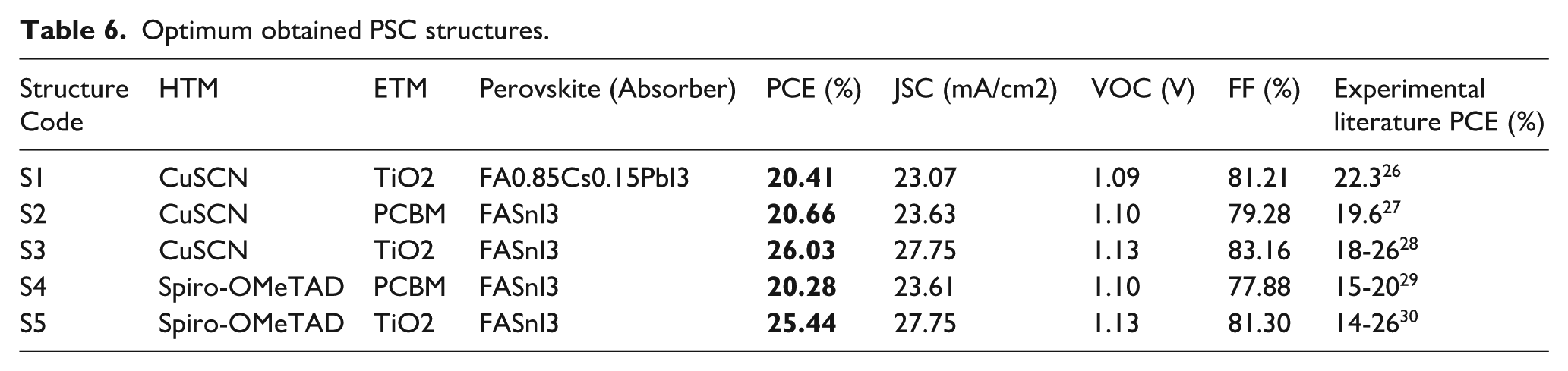
optimum obtained PSC structures.

Layer property optimization
In the second phase, the optimum PSC structures listed in Table 6 were considered candidates for optimization from the perspective of layer properties. The effect of varying important parameters of the absorber layers, including their thickness and doping density, was investigated. The photovoltaic parameters and recombination factor variations are presented as functions of layer properties for S1–S5 structures (Table 6). The photovoltaic parameters refer to the performance factors listed in Tables 5–6 and Table S1. The recombination factor refers to the recombination peak observed in recombination path plots for each property value. Due to the large amount of data and diagrams for each structure, only the S3 structure results are reported here. Further discussion is provided below.
Perovskite thickness
Using the SCAPS-1D batch study, the effect of perovskite thickness variation was investigated. The effect of varying the perovskite thickness from 100 nm to 1000 nm on the photovoltaic parameters and recombination factor is shown in Figure 1 for the S3 structure.

Variation of photovoltaic parameters and recombination factor as a function of perovskite thickness for the S3 PSC structure.
As shown in Figure 1, increasing perovskite thickness generally has a positive impact on performance parameters. Nevertheless, the recombination rate peak also increases. This behavior can be explained by the literature. 31 As perovskite thickness increases, electron-hole generation is enhanced. On the other hand, recombination probability also rises. The VOC and JSC refer to recombination and generation, respectively. This justifies the behaviors observed in Figure 2. According to the efficiency plot in Figure 1, the efficiency increment rate decreases after a thickness of 500 nm. This observation helps in selecting the proper thickness, balancing recombination effects. Hence, a thickness of 500 nm appears to be the optimum choice for the perovskite layer.
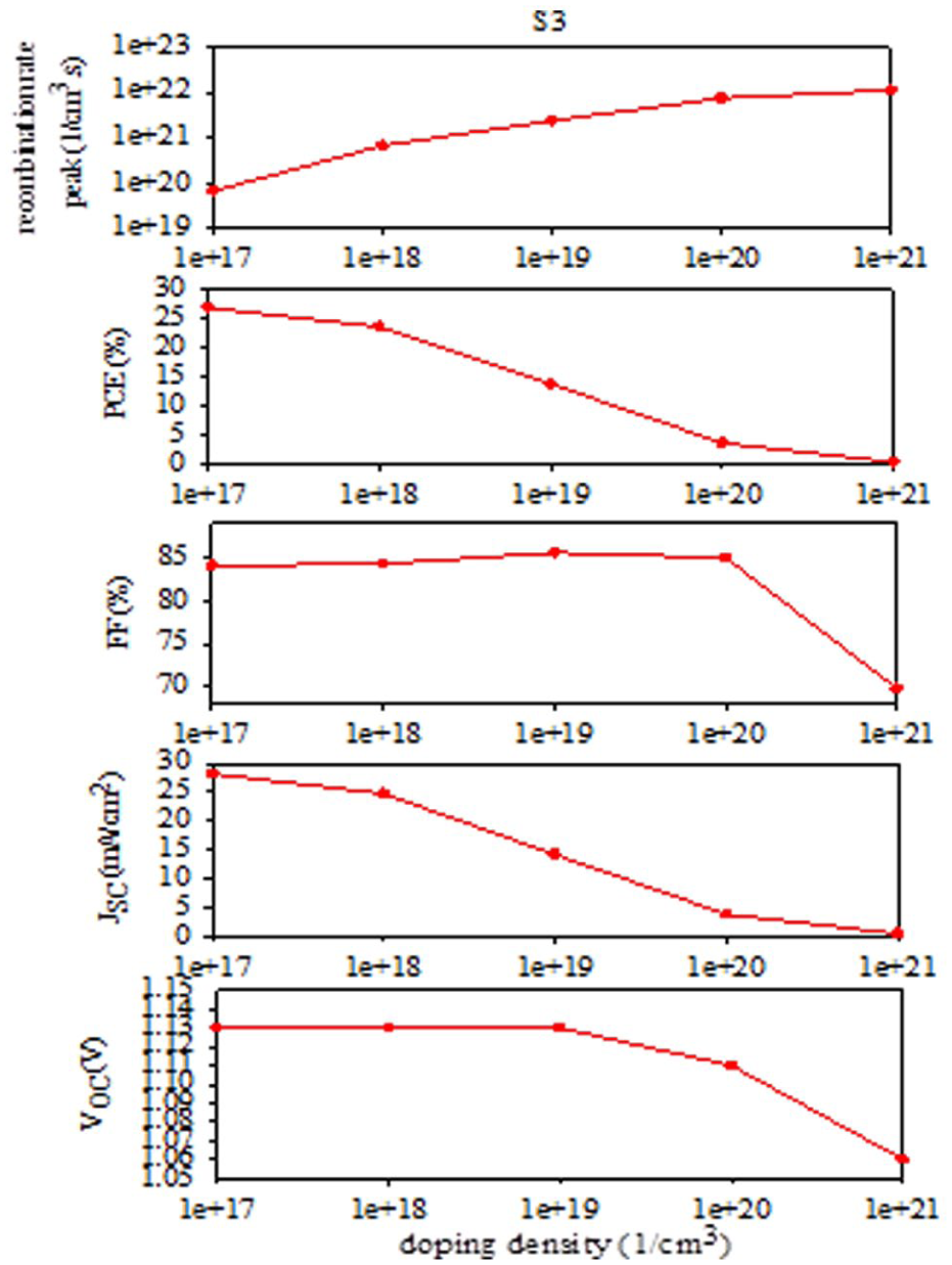
Variation of photovoltaic parameters and recombination factor as a function of perovskite doping density for the S3 PSC structure.
Perovskite doping
The doping density of a layer is another important parameter. It refers to the concentration of impurities in a material. These impurities can be either acceptors or donors, corresponding to positive and negative doping, respectively. Therefore, doping density directly affects the charge concentration in a material and, consequently, the cell’s performance.
In this study, the effect of perovskite doping density was investigated over the range of 1017-1021 1/cm3 for the S3 structure. Figure 2 shows the results in terms of performance and recombination parameters.
The diagrams in Figure 2 reveal similar trends across the variation of doping density. The performance parameters show a descending trend with increasing doping density, which can be attributed to increased recombination. Enhancing the doping density of the absorber layer facilitates greater charge carrier generation; however, beyond a threshold value, it also leads to more charge recombination. Based on the obtained results, the lowest doping density range appears to be the optimum value for all S1–S5 PSC structures considered in this study.
Working point optimization
In addition to the aforementioned layer parameters that were investigated, some general simulation conditions should be considered due to their importance. In the following, some of these general conditions will be discussed.
Temperature
The temperature of solar cells is one of the crucial conditions that should be calibrated properly. Its optimization can help experimental studies to be performed under more suitable conditions. It appears that the simulation process can be employed effectively in this case. Therefore, in the present case, we selected the temperature range of 300–400 K to determine an optimal temperature. The results in Figure 3 for S3 indicate the effect of temperature on the performance parameters of PSCs.
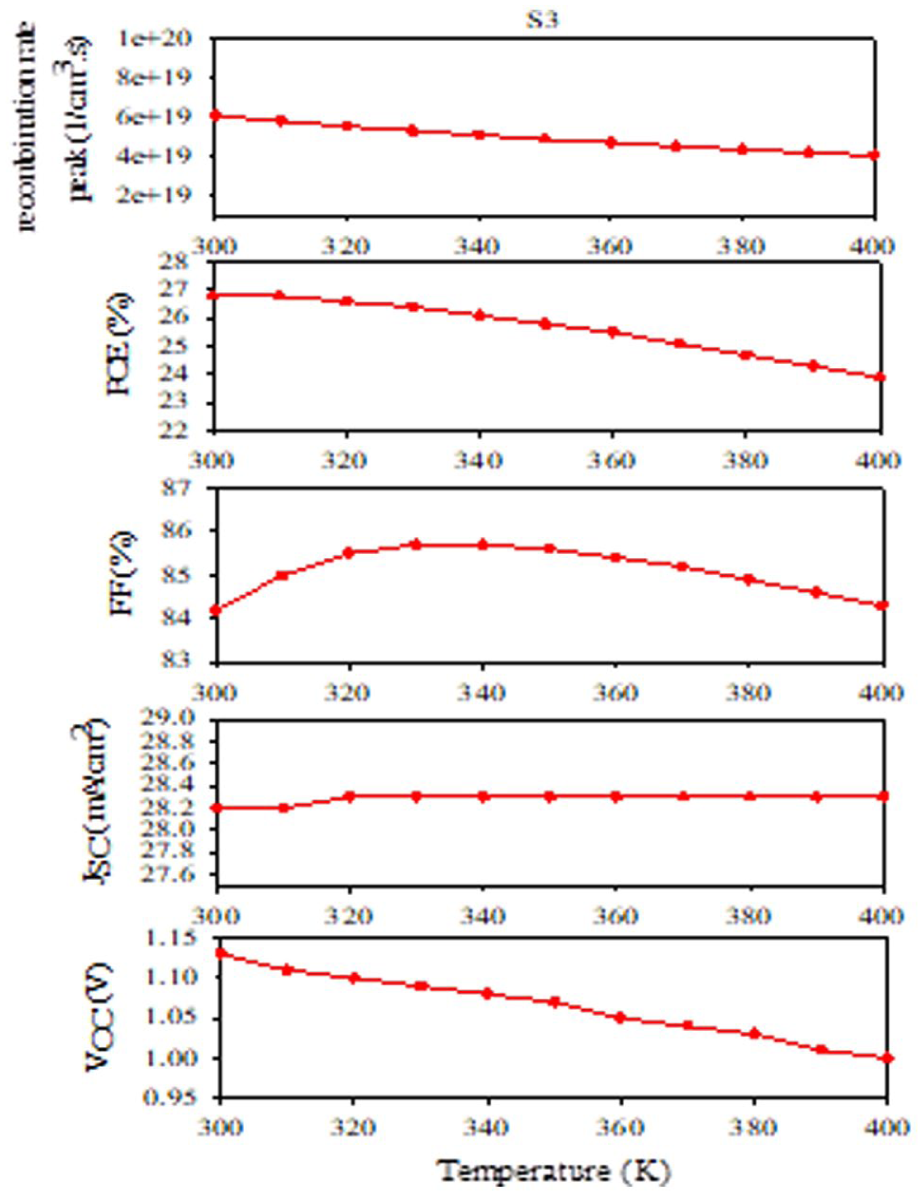
Variation of photovoltaic parameters and recombination factor as a function of temperature for the S3 PSC structure.
According to the results obtained for the S1-S5 structures, a generally descending behavior is observed with increasing temperature. Therefore, selecting lower temperatures will lead to better performance results. We considered a temperature of 300 K for all of the studied structures. This can be attributed to the higher mobility of charge carriers at elevated temperatures, which leads to greater heat dissipation and lower performance.
However, Figure 3 demonstrates that the short-circuit current density (JSC) exhibits only a weak dependence on temperature. This behavior can be explained by the intrinsic electronic structure of the FASnI₃ absorber. The perovskite bandgap shows a very small temperature coefficient, resulting in only minor shifts in the absorption edge as the temperature increases. As a result, the photogeneration rate remains nearly unchanged. In addition, the high absorption coefficient of tin-based perovskites ensures that small variations in bandgap or phonon interactions do not significantly influence photon absorption. Although higher temperatures generally enhance recombination, the thermal activation of carrier mobility and diffusion partially offsets these losses, preserving the overall charge-collection efficiency.
Series resistance
The operational mechanisms of solar cells are affected by parasitic resistances existing in their circuits. These resistances include series and shunt resistances. They are related to electron and hole generation and recombination mechanisms. Generally, series resistance and shunt resistance represent a cell’s resistance to the generation and recombination processes, respectively.10,32 Lower values are optimal for series resistance, whereas higher values are optimal for shunt resistance. In this case, the effect of series resistance was investigated in the range of 0.1-1 Ω.cm2. The results are presented in Figure 4 for the S3 PSC structure. It should be noted that the mentioned resistances do not have significant effects on recombination. Therefore, we preferred not to report them.

Variation of photovoltaic parameters and recombination factor as a function of series resistance for the S3 PSC structure.
According to the results, variation of series resistance will lessen the PCE and FF but do not change VOC and JSC anymore. At short-circuit (V = 0) the photocurrent is set by the photogeneration rate and the diode/shunt terms; the Rₛ-dependent voltage drop (I·Rₛ) is negligible for typical Rₛ values in perovskite devices, so JSC changes only marginally. At open-circuit (I = 0) there is no current so no I·Rₛ voltage drop hence VOC follows the diode balance (≈ nVₜ ln(IL/I₀ + 1)) and is essentially independent of Rₛ. 33 As mentioned above, lower values are desirable for series resistance. The results in Figure 5 confirm this as well.
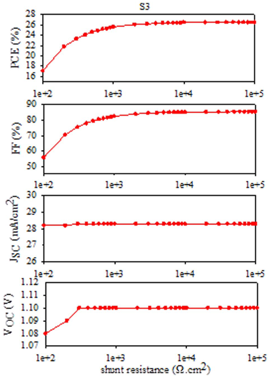
Variation of photovoltaic parameters and recombination factor as a function of shunt resistance for the S3 PSC structure.
Shunt resistance
As mentioned earlier, higher values of shunt resistance are desirable for a solar cell. As the shunt resistance increases, the cell approaches an ideal solar cell with infinite shunt resistance. To confirm this concept, we considered a relatively wide data range of 102-105 Ω.cm2 to investigate the effect of shunt resistance. However, beyond a threshold value, further increments do not occur. The diagrams in Figure 5 for S3 confirm this observation.
Reflection
In most simulation studies, reflection parameters are not considered, and the calibrations remain far from real conditions. However, in SCAPS-1D, this parameter can also be included. The reflection parameter indicates the percentage of light transmitted to the absorber layer. It is evident that with increasing reflection, the amount of absorbed light decreases, leading to lower performance. The diagrams in Figure 6 for the S3 PSC structure confirm this. However, on the other hand, lower electron-hole generation can also lead to reduced recombination. Therefore, as shown in the diagrams, a decrease is observed in recombination plots. Hence, selecting the optimum reflection depends on the objective of the study—whether to prioritize higher performance or lower recombination.
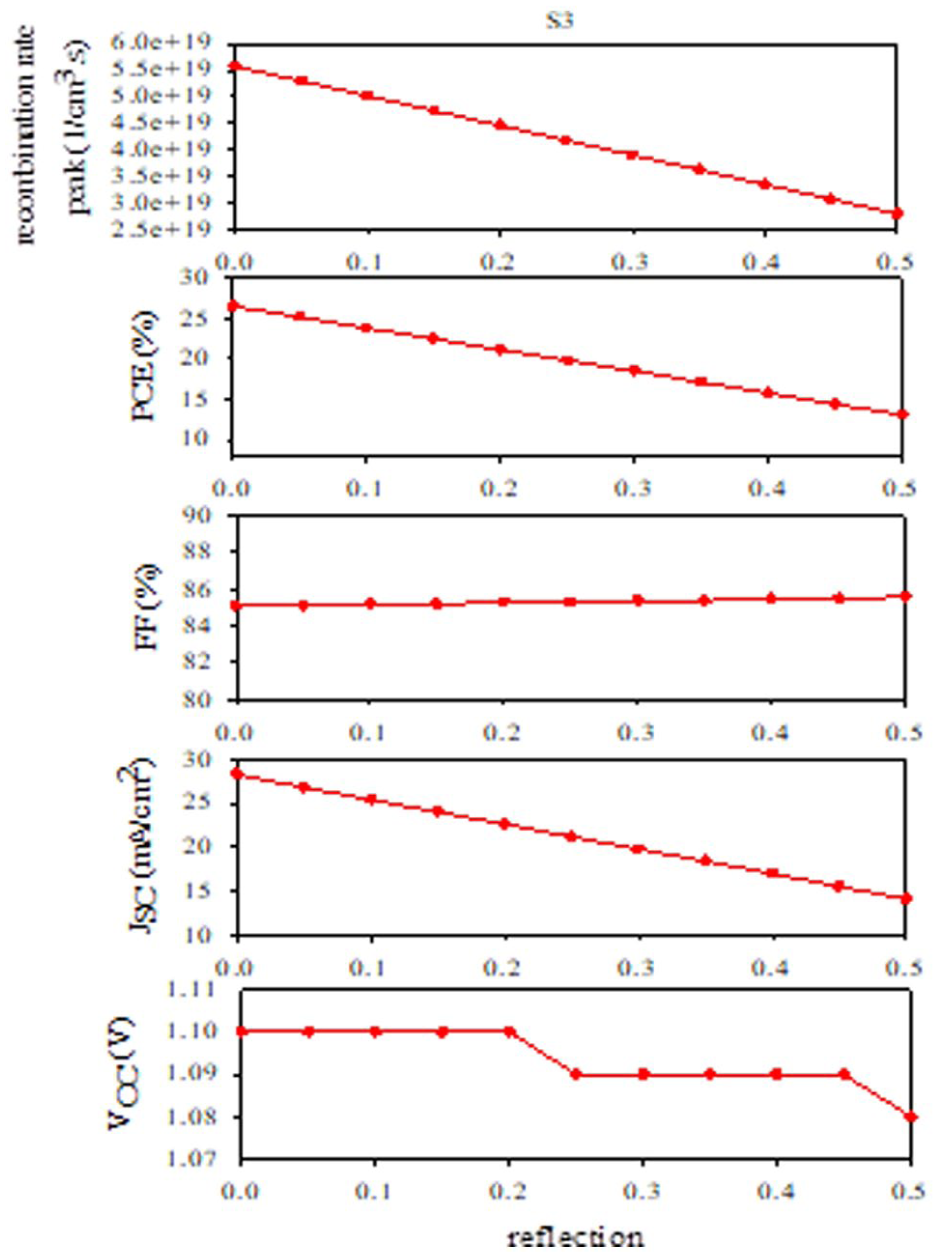
Variation of photovoltaic parameters and recombination factor as a function of reflection for the S3 PSC structure.
Final I-V results
To gain better insights, it is useful to summarize the obtained results. The total efficiency increased by about 1%. However, it should be noted that in this study the recombination factor was considered in addition to the performance factors during the optimization processes, which led to smaller efficiency increments. As a final result, it is better to choose a higher value for absorber thickness, lower for absorber density, lower series resistance, and higher shunt resistance. According to the software calculations, it is obvious to choose no reflection, but it should be considered as the experimental cell value to approach it to the real conditions.
The thickness effects observed in our SCAPS-1D simulations are consistent with experimental reports. Experimental studies on MAPbI₃ devices show an optimum absorber thickness in the few-hundred-nanometer range (for example ≈330 nm reported by Liu et al. 34 ), where JSC is high enough while recombination and transport losses remain limited. Thicker films increase optical absorption (and can raise the radiative VOC limit), but can also increase bulk recombination, series resistance and processing-related coverage/strain issues—effects which have been documented experimentally. We therefore compare our simulated trends to these experimental findings.34 –38 It is well-known that other parameters such as transport-layer conductivity (series/shunt resistance), defect/trap density, and operating temperature crucially affect real-world device performance. For example, high series resistance or low shunt resistance degrade the fill factor (and thus efficiency), even if the absorber is optimally thick. Similarly, elevated operating temperatures accelerate recombination and increase resistive losses, reducing Voc, FF and overall PCE. On the other hand, although electronic doping of the perovskite bulk is often negligible in lead-halide perovskites, trap/defect densities and transport-layer conductivity remain key. Therefore, our SCAPS-1D predictions should be interpreted as the “idealized” limit (assuming low parasitic losses and stable temperature), and further work (simulation + experiment) should address these non-idealities for realistic optimization.39 –41
To provide further insight, the total I-V curves of different processes are given in Figure 7.

I-V plots of different stages of optimization of the S3 PSC structure.
The area under the I-V curve of a solar cell represents its performance. It is evident from the I-V plots that this area increased with the progression of the optimization processes. This confirms the overall positive outcome of the present study. The results were in good agreement with the similar experimental works.18,42
Conclusion
In summary, this study presented theoretical investigations on perovskite solar cell simulation using the SCAPS-1D simulation package. Considering the vast variety of possible perovskite solar cell structures, this study was based on selecting proper PSCs among the proposed structures. For this purpose, 8 different MA-based and FA-based absorbers were considered. Moreover, various organic and inorganic materials, including TiO2, ZnO, and PCBM as ETMs, and CuSCN, PEDOT:PSS, and Spiro-OMeTAD as HTMs, were used to form 72 unique PSC structures. Among these, 5 structures were selected as good data (efficiency above 20%) for further investigation. The most suitable structure obtained as CuSCN/TiO₂/FASnI₃ attaining a maximum power conversion efficiency of 26.03%, accompanied by a short-circuit current density of 27.75 mA·cm⁻², a corresponding open-circuit voltage of 1.13 V, and a fill factor of 83.16%. Optimization of these selected structures was performed based on appropriate layer properties and working points. In general, for property optimization, relatively higher thicknesses were proposed for perovskite layers, while lower values were suggested for doping densities of the perovskite layer. For working point optimization, it was demonstrated that low temperatures and series resistances, together with high shunt resistances, are desirable for PSCs.
Supplemental Material
sj-docx-1-chl-10.1177_17475198261428588 – Supplemental material for Promotion of a perovskite solar cell structure by optimizing several parametric factors in the SCAPS-1D simulation environment
Supplemental material, sj-docx-1-chl-10.1177_17475198261428588 for Promotion of a perovskite solar cell structure by optimizing several parametric factors in the SCAPS-1D simulation environment by Nagihan Delibaş in Journal of Chemical Research
Footnotes
Acknowledgements
The Scientific Research Projects Coordinator of Sakarya University is greatly acknowledged. The author is grateful to the participating institutions, which is Sakarya University. The author also acknowledges the Research Square regarding the presence of the current article there since 19 October 2023. The mentioned pre-print version was entitled as “
Ethical considerations
Ethical approval is not applicable for the article. as it did not engage human participants or animals and was based exclusively on raw materials.
Consent to participate
Not applicable. This research did not include the direct involvement of human participants.
Consent for publication
Not applicable. This study does not include any data pertaining to individual persons in any format.
Author contributions
The author agrees to be accountable for the content and conclusions of the article. This study has only one author, with contributions as follows: All contributor roles—including Conceptualization, Data curation, Formal analysis, Funding acquisition, Investigation, Methodology, Project administration, Software, Resources, Supervision, Validation, Visualization, Writing—original draft, and Writing—review & editing—were performed by Nagihan Delibas.
Funding
The author disclosed receipt of the following financial support for the research, authorship, and/or publication of this article: This work was supported by the Sakarya University.
Declaration of conflicting interests
The author declared no potential conflicts of interest with respect to the research, authorship, and/or publication of this article.
Data availability statement
The data generated in this study are available within the article and its supplementary data files or upon request from the corresponding author.
Statement of informed consent
There are no human subjects in this article, and informed consent is not applicable.
Preprint
A preprint has previously been published by Nagihan Delibas in 2023 [35]
Supplemental material
Supplemental material for this article is available online.
References
Supplementary Material
Please find the following supplemental material available below.
For Open Access articles published under a Creative Commons License, all supplemental material carries the same license as the article it is associated with.
For non-Open Access articles published, all supplemental material carries a non-exclusive license, and permission requests for re-use of supplemental material or any part of supplemental material shall be sent directly to the copyright owner as specified in the copyright notice associated with the article.