
Abstract
Perovskite solar cells have been attracted as new representatives for the third-generation photovoltaic devices. Simple strategies for high efficiency with the long-term stability of solar cells are the challenges for commercial solar cell technology. Another challenge of the development toward industrial scale in perovskite solar cells is the production under the ambient and high humidity. In this sense, we successfully fabricated perovskite solar cells via solution depositions of all layers under ambient air with a relative humidity above 50%. Titanium dioxide (TiO2) nanoparticles with the roles for efficient charge extraction and electron transportation properties were used as an electron-transporting layer in the cell fabrication. The modification of TiO2 nanoparticles for energy band adjustment was done by doping with nontoxic cadmium sulfide (CdS) quantum dots. With the variation of CdS concentrations, energy band is not only changeable, but the enhancement of the perovskite solar cells efficiency could be achieved compared with the conventional cells made of pristine-TiO2 film and TiO2 nanoparticles.
Keywords
Introduction
Organic–inorganic halide perovskite, mainly methylammonium lead halide CH3NH3PbX3 (X = Cl−, Br−, and I−)-based one, recently shows high power conversion efficiency (PCE) of photovoltaic applications. 1,2 The existent characteristics of perovskite with high absorption coefficient, good charge carrier mobility (approximately 10 cm2/Vs), and large electron–hole diffusion length (0.1–1.0 μm) are potential to improve the PCE of the devices. 3 –5 The superior perovskite material properties have been devoted from both mesoporous and simple planar perovskite designs. 6
Typical perovskite solar cells are composed from a transparent conducting layer (fluorine-doped tin oxides (FTO) or indium tin oxides) with a perovskite material as an active film sandwiched between an electron-transporting layer (ETL) and a hole-transporting layer (HTL). The cells have two common architectures, that is, n-i-p and p-i-n junctions for ETL/perovskite/HTL and HTL/perovskite/ETL, respectively. 6,7 The important function of common ETL, such as titanium dioxide (TiO2) and zinc oxide (ZnO), can provide an electron pathway from perovskite to electrode and also reduce recombination rate of electron–hole pairs. 8,9 It should be noted that most efficient planar perovskite cells were fabricated using TiO2 thin films as the ETL. 10
High PCEs of over 20% of perovskite solar cells have been reported for only with the laboratory scales within a few years ago. 11 –14 Remarkably, the reported certified PCEs of perovskite solar cells at 25.2% from the National Renewable Energy Laboratory (NREL) chart 15 are catching up the PCEs of silicon solar cells. Besides highly efficient performance, perovskite solar cells are still facing a poor stability issue, where rapid degradation occurs under high humidity environments. 16,17
Several works reported the perovskite cells with relatively small areas fabricated under nitrogen (N2) atmosphere. For example, high efficiency of perovskite solar cells of approximately 23% (with the active area of approximately 0.09 cm2) was reported by Jeon et al. 18 Anaraki et al. developed the efficient performance of planar perovskite solar cells with PCE closed to 20% with an active area of 0.16 cm2. 19 Anyway, the fabrication of the perovskite cells under the ambient air condition always shows the lower PCEs of the cells. Xu et al. achieved the fabrication of planar perovskite solar cell configuration with Cs0.15FA0.85PbI3 as perovskite films under ambient air atmosphere, but the PCE was quite low. 20 Yang et al. studied an effect of relative humidity (RH) on perovskite solar cells fabricated via a blade-coating technique under ambient air. They reported that PCE of approximately 10% could be achieved from the cells made in RH ranging from 15% to 25%, while cells provided the lower PCEs of 3.63% and 0.35% under 40–50% RH and 60–70% RH, respectively. 21 Mohamad et al. reported that perovskite solar cells with an inverted structure configuration made under air condition using spray-coating approach showed lower PCE compared with those prepared under N2 condition. 22 Therefore, fabrications of perovskite solar cells at the ambient air atmosphere have still been focused and developed by many researchers. In other words, the fabrication of the completed perovskite cells without an inert gas-filled glovebox under high RH conditions is a crucial challenge. In addition, the chemical instability of perovskite absorber layer has been a significant obstacle to the commercialization of solar technology.
Limitation of perovskite solar cell efficiency is not only that an active layer is easily destroyed in the presence of UV light, heat, and air moisture, but the TiO2-based ETL layer is generated superoxide radicals from a dynamic photocatalytic behavior, resulting in the instability of the perovskite layer. 23 –26
Quantum dots (QDs), fine semiconductor particles with the size in a few nanometers, that have optical and electronic properties that differ from bulk particles because of quantum mechanics, are promising materials for various photovoltaic applications. This is because the bandgap of QDs can be tuned by size controlling and the extinction coefficient of QDs can enhance the light-harvesting ability for improving efficiency. Nontoxic cadmium sulfide (CdS) is a QD material that is chemically stable with a direct bandgap of 2.4 eV and excellent electron transport ability. In this sense, CdS-modified TiO2 (CdS/TiO2) is an expected material to be a good component for photovoltaic applications. 27,28 According to the energy band arrangement of CdS/TiO2 nanocomposite, the excited electron from the conduction band of TiO2 can migrate to CdS, resulting in lower recombination rates caused by photocatalytic behavior of TiO2. 26,29
CdS/TiO2 films have been prepared by various methods, including atomic layer deposition, 26,29 spin coating, successive ionic layer adsorption, and reaction, 30 –32 while pristine CdS has been reported to be prepared by thermal evaporation 33 and chemical bath deposition methods. 34,35 These techniques are quite complicated, so the alternative methods have been under development.
For metal oxide nanoparticles employed for perovskite photovoltaic devices, the uses of anatase single-crystalline TiO2 nanoparticles, compact TiO2, and mesoporous TiO2 as ETLs could enhance PCE. 36,37 Najafi et al. demonstrated utilizations of ZnO and NiO x nanoparticles as ETL and HTL, respectively, for the inverted perovskite solar cells. 38 From the opened literature, there is no report on the uses of insertion of CdS/TiO2 nanoparticles in planar perovskite solar cells as ETL and the fabrication of the cells under ambient air.
In this work, synthesis of TiO2 nanoparticles via sol-hydrothermal method is reported. The TiO2 nanoparticles are used as ETLs for perovskite photovoltaic devices, where all deposited solution layers are successfully fabricated under an open-air atmosphere. Modification of TiO2 nanoparticles by CdS QDs is revealed. The effect of variation of CdS concentrations on the efficiency of the perovskite solar cells is studied. Note that this work does not focus on the development of very high state-of-the-art efficiency in perovskite solar cells. The preparation of the planar perovskite solar cells under an open-air condition for the potential development in the tropical and humid countries and the use of CdS/TiO2 nanoparticles as ETLs are reported instead.
Materials and methods
Materials
Tetrabutyl titanate (reagent grade, 97%), calcium nitrate tetrahydrate (Cd(NO3)2.4H2O, 99%), acetylacetone (CH3CH2COCH2CH3), and sodium sulfide nonahydrate (Na2S.9H2O, 98%), for preparation of CdS-doped TiO2 nanoparticles, were purchased from Sigma-Aldrich. For perovskite fabrication, titanium diisopropoxide bis(acetylacetonate) (75 wt% in isopropanol), methylammonium iodide (anhydrous MAI, >99%), lead (II) iodide (PbI2, 99.999%), 4-tert-butyl pyridine (98%), lithium bis(trifluoromethanesulfonyl)imide (99.95%), N, N-dimethyl sulfoxide (anhydrous DMSO, 99.9%), 2,2′,7,7′-tetrakis[N, N-di(4-methoxyphenyl)amino]-9,9′-spirobifluorene, spiro-OMeTAD (high performance liquid chromatography (HPLC) grade, 99%), N, N-dimethylformamide (anhydrous DMF, 99.8%), and chlorobenzene (anhydrous, 99.8%) were obtained from Sigma-Aldrich (Germany).
Synthesis of CdS-doped TiO2 nanoparticles
TiO2 nanoparticles were synthesized via sol-hydrothermal method. 39 Tetrabutyl titanate (4.3 mL) was mixed with acetylacetone (1.3 mL) (mole ratio is 1:1). Isopropyl alcohol (20 mL) and deionized (DI) water (30 mL) were slowly dropped into the mixture under magnetic stirring. Cd(NO3)2.4H2O (2, 4, 6, 8, and 10 wt%) was then mixed to the mixture. The mixed solution was kept by hydrothermal treatment at 80°C for 12 h. The solution was dried in an oven at 80°C overnight and calcined at 500°C for 3 h to form cadmium oxide (CdO)/TiO2 powders. Afterward, Na2S.9H2O (0.02, 0.04, 0.06, 0.08, and 0.10 g) was dissolved into DI water (100 mL). CdO/TiO2 (0.6 g) was dispersed in the obtained Na2S solution for 6 h. 40 The CdS products were filtered and dried overnight at 80°C.
Fabrication of perovskite photovoltaic cells
Patterned FTO substrates were ultrasonically cleaned by a detergent, DI water, acetone, and isopropanol. UV treatment was then carried out for 30 min. CdS-doped TiO2 nanoparticles were mixed in the TiO2 precursor (0.3 M titanium diisopropoxide bis(acetylacetonate) in butanol solution). The mixed solution was spun cast on FTO at 4000 r/min for 20 s to form the ETL. To smoothen the surface of this layer, titanium diisopropoxide bis(acetylacetonate) solution was then coated on the CdS-doped TiO2 layer at 4000 r/min for 20 s. The samples were annealed in air at 500°C for 40 min, cooled down at room temperature, and then treated by UV light for 30 min prior to use.
To prepare the perovskite (CH3NH3PbI3) films with a one-step approach, a perovskite precursor solution containing PbI2 (1 mole) and MAI (1 mole) in anhydrous DMF:DMSO (volume ratio = 8:2) was prepared under N2 atmosphere in a glovebox. The solution was coated on the CdS-TiO2 layers at 2000 r/min for 30 s under open-air atmosphere (outside the glovebox). To complete the active layers, ethyl acetate (EA) solution was dropped onto the prepared substrates. 41 The perovskite films were heated at 100°C for 10 min. The spiro-OMeTAD solution as HTL was spin-coated on the perovskite surface at 3000 r/min for 30 s. The solution consisted of 72.3 mg spiro-OMeTAD, 28.8 µL of 4-tert-butyl pyridine and 17.5 µL of lithium bis(trifluoromethanesulfonyl)imide (Li-TFSI) solution (520 mg Li-TFSI in 1 mL acetonitrile) in 1 mL of chlorobenzene. Finally, silver (Ag) electrode was deposited by thermal evaporation. The active area of the cells was 0.04 cm2. The devices were also prepared under N2 atmosphere in a glovebox for comparisons.
Characterizations and photovoltaic measurements
The optical absorptions of TiO2 and CdS/TiO2 nanoparticles were measured by a JASCO V-550 UV-vis spectrophotometer. Photoluminescence (PL) emission spectra of samples were monitored by a JASCO FP-8600 spectrofluorimeter under an excitation wavelength of 450 nm. Transmission electron microscopy (TEM, JEOL JEM-2010, Japan) was used to observe morphological appearance of the CdS-doped TiO2 nanoparticles. A cross-sectional image of the perovskite cells was taken by field-emission scanning electron microscopy (FESEM, JEOL JSM-7001F, Japan). Fermi levels of TiO2 and CdS/TiO2 nanoparticles were measured by photoelectron spectroscopy in air using a Riken Keiki AC-3 instrument, Japan. Photovoltaic measurements of the solar cells were performed using WXS-155S-L2 machine with a solar simulator (Wacom Electric Co., Ltd, Tokyo, Japan) under the light intensity of 100 mW cm2 (AM 1.5 G). At least three cells were used for tests in each condition. X-Ray diffraction (XRD) patterns were performed using a Rigaku Smartlab machine with copper Kα radiation (λ = 0.15418 nm). Average crystallite sizes of samples were calculated by following Scherrer equation (1)

where D is crystallite size, K is a coefficient (0.94), λ is the wavelength of X-ray radiation, and β is full-width at half-maximum intensity of a typical peak, and θ is the diffraction angle.
Results and discussion
TiO2 and CdS QDs-modified TiO2 nanoparticles were successfully prepared by sol-hydrothermal method. 39 Figure 1(a) shows the UV-vis spectra of the TiO2 nanoparticles without and with CdS at various concentrations (i.e. 2%, 4%, 6%, 8%, and 10%). The pristine TiO2 nanoparticles exhibit absorption spectrum in the UV range (below 380 nm). CdS QDs significantly cause red shifts in the optical absorption edges, which provide better light harvesting in the visible range of 400–550 nm. The absorption toward longer wavelength indicates that CdS QDs are indeed embedded in TiO2 nanoparticles and composed on the surface of TiO2. 40 At high concentration of doping (i.e. 8% and 10% CdS), the absorption intensity is not much changeable due to the limited loading amount of CdS onto the TiO2 nanoparticles.

Optical properties of TiO2 nanoparticles without/with CdS: (a) UV-vis spectra and (b) PL spectra. TiO2: titanium dioxide; CdS: cadmium sulfide; PL: photoluminescence.
PL emission spectra of pristine TiO2 nanoparticles and the CdS QDs-modified TiO2 nanoparticles with interval wavelength between 350 nm and 800 nm were monitored at room temperature with a JASCO FP-8600 spectrofluorimeter under excitation wavelength at 270 nm, as shown in Figure 1(b). The CdS QDs-modified TiO2 showed quenching (reduction of PL intensity) compared with pristine TiO2. The higher doping, the higher quenching, is observed. Low PL intensities of TiO2 nanoparticles were found at CdS doping of 8% and 10%. This quenching phenomenon indicated that the charge separation process is effectively occurred by the electron transfer from the conduction band of CdS to the conduction band of TiO2 with low recombination rate. 33,35,36
Figure 2 shows XRD patterns of the TiO2 nanoparticles without and with CdS QDs (2%, 6%, and 10%). The characteristic peak positions at 25.3 (101), 37.6 (004), 47.9 (200), 54.7 (105), 62.7 (204), and 75.1 (215) appeared in all samples, corresponding to the anatase-TiO2 phase. 42,43,44 The expected characteristic peak of CdS was not found in all different conditions because of the high dispersion with the quantum size effect of CdS QDs. 40,45 Nevertheless, the main diffraction peaks of TiO2 presented slight shifts to lower 2θ positions for CdS-modified TiO2. This implies that the doping Cd2+ element was incorporated into the structures of TiO2 or substituted the position of titanium ions. 46 Crystallite sizes of samples were calculated by the Scherrer equation (Table S1 in Supporting Information). The particle sizes were found to be 7.1–10.4 nm with relatively uniform size dispersion. These particle sizes are corresponding to the crystallite size estimated from TEM images (Figure 3). From Table S1 in Supporting Information, the crystallite size of TiO2 nanoparticles was about 7.1 nm. With the introduction of CdS QDs on TiO2 nanoparticles, the crystallite sizes were found to increase because of the formation of agglomerated nanoparticles. 47 The crystallite sizes of the CdS QDs-modified TiO2 with 2%, 6%, and 10% doping were 10.26, 10.41, and 8.09 nm, respectively. To confirm the existence of CdS on TiO2 nanoparticles, the Cd and S elements were determined by SEM energy-dispersive X-ray spectroscopy (see Figure S1 in Supporting Information). Figure S2 in Supporting Information presents the EDX spectra of CdS/TiO2 at 2%, 4%, 6%, 8%, and 10% compared with TiO2 nanoparticles.

XRD diffraction patterns of TiO2 nanoparticles with/without CdS with reference peaks of CdS powder, anatase-TiO2 nanoparticles, and rutile-TiO2 nanoparticles. TiO2: titanium dioxide; XRD: X-ray diffraction; CdS: cadmium sulfide.

TEM images and the lattice fringes of (a, c) pristine TiO2 and (b, d) CdS QDs-modified TiO2 nanoparticles. TiO2: titanium dioxide; CdS: cadmium sulfide; QD: quantum dot; TEM: transmission electron microscopy.
Figure 3(a) and (b) illustrates TEM images of TiO2 nanoparticles with/without CdS, which indicate the shapes of nanocrystals. It was assessed whether the size of the 10% CdS QDs-modified TiO2 was not quite different from unmodified TiO2. The size distributions of both samples are also not significantly different (Figure S3 in Supporting Information). The d-spacing of lattice fringes of TiO2 nanoparticles was found as 0.352 nm, corresponding to the lattice plane of (101) anatase TiO2 structure, as shown in Figure 3(c). To confirm again the existence of CdS QDs and the formation of CdS/TiO2 heterostructure, the distinct lattice fringes of the CdS QDs-modified TiO2 with d-spacing values of 0.337 and 0.217 nm were observed, correlating with the lattice plains of CdS at (111) and (220), respectively (Figure 3(d)). 48,49
Planar perovskite solar cells with a typical device architecture of FTO glass/TiO2 (as ETL)/CH3NH3PbI3/spiro-OMeTAD (as HTL)/Ag were fabricated under N2 atmosphere in a glovebox (Figure 4(a)). A cross-sectional SEM image of the completed perovskite cells on a rigid FTO glass is shown in Figure 4(b). The perovskite function is a core of devices that generate electrons and holes after light harvesting. The FESEM image of the dense CH3NH3PbI3 perovskite surface with EA as antisolvent is presented in Supporting Information (Figure S4). From various tested cells, a champion PCE of 8.16% (with a small area of 0.04 cm2) with an open-circuit voltage (V oc), a short-circuit current density (J sc), and a fill factor (FF) of 0.87 V, 15.25 mA/cm2, and 0.61, respectively, was obtained, as shown in Figure 5 (other test results can be seen from Table S2 in Supporting Information). From a previous work, Deng et al. fabricated perovskite solar cells using a modified blade coating. The perovskite solar cells with a PCE of approximately 20% (an active area of 0.075 cm2) were achieved under an average annual humidity of 68% in Lincoln (Nebraska, USA). 14 In the reported work, surfactants were added into perovskite solution to prevent the moisture on the surface of perovskite layer. The hydrophilic group of the surfactants interacts with perovskite, while the hydrophobic group interacts with the atmosphere on the opposite side. 14 Anyhow, the country humidity is one of the main factors affecting performance and stability of the devices. As mentioned above, the performance and stability of the devices in this study have been dramatically changed when exposed to excessive humidity as an annual average humidity in Thailand is about 78%, 50 which is higher than the study of Deng et al. 14

(a) Device architecture of planar perovskite solar cells with different ETLs made of only TiO2 film, with the inserted TiO2 nanoparticles, and with the inserted CdS/TiO2 nanoparticles. (b) A cross-sectional SEM image of a perovskite solar cell with CdS QDs. CdS: cadmium sulfide; SEM: scanning electron microscopy; QD: quantum dot; ETL: electron-transporting layer; TiO2: titanium dioxide.

J-V curves of perovskite solar cells fabricated under N2 and open-air atmospheres (the curves shown are selected from the highest PCEs from three cells tested). PCE: power conversion efficiency.
To realize the effect of open-air condition to study the potential for fabrication of perovskite solar cells for practical scales, the reference cells with the same structure as described above were fabricated outside the glovebox. It was found that PCE of the cell dramatically reduced to 1.33% (about 84% reduction) with V
oc, J
sc, and FF of 0.70 V, 5.84 mA/cm2, and 0.32, respectively. Open-air atmosphere containing moisture (RH approximately 50% in this work) and oxygen causes the degradation of perovskite absorber (MAPbI3) films to form PbI2 and MAI, because of high polarity of H2O.
16,17,51
Normally, in the perovskite composition,
Perovskite solar cells made of CdS QDs-modified nanoparticles as ETL for charge extraction, as shown in Figure 4(a), were fabricated. The cells made of TiO2 film and pristine-TiO2 nanoparticles were also studied as the references. Figure 6(a) shows the corresponding current density–voltage (J-V) curves of perovskite solar cells made of films and the inserted particles. Photovoltaic characteristics are listed in Table 1. The cell made of TiO2 film revealed V oc, J sc, and FF of 0.75 V, 5.21 mA/cm2, and 0.30, respectively, with PCE of 1.18%. The device made of TiO2 nanoparticles showed decreases of V oc and FF to 0.61 V and 0.29, respectively, while J sc was found to increase to 6.70 mA/cm2. This is because of the benefit of larger interfacial areas of nanoparticles compared with the film. However, there was not much change in PCE compared with that made of the film.

(a) J-V curves of perovskite photovoltaic devices with several ETLs and (b) schematic diagrams of band alignments and charge recombination in the cells. ETL: electron-transporting layer.
Photovoltaic characteristics of perovskite photovoltaic devices made of several ETLs under ambient air.

ETL: electron-transporting layer; CdS: cadmium sulfide; TiO2: titanium dioxide; FF: fill factor; PCE: power conversion efficiency.
To determine the energy bandgap of samples, Tauc’s plot was carried out using indirect allowed transitions (n = 2) (Figure S6 in Supporting Information). The bandgaps of the pristine TiO2 and CdS/TiO2 with 2%, 4%, 6%, 8%, and 10% doping are approximately 3.00, 2.45, 2.30, 2.20, and 2.18 eV, respectively, as shown in Figure 6(b). With increasing CdS concentrations in TiO2, narrower bandgaps compared with pristine TiO2 were presented. Fermi levels of the obtained samples were measured by photoelectron spectroscopy in air (Figure S7 in Supporting Information). It was found that the Fermi level of TiO2 with CdS QDs was slightly changed and compared with the pristine one.
The device with 2% CdS/TiO2 exhibited a champion PCE of 2.40% with V oc, J sc, and FF of 0.62 V, 13.05 mA/cm2, and 0.30, respectively. J sc was significantly increased and also revealed more excited electrons as well as reduced interfacial charge recombination. 53 This result is in line with the UV-vis absorption and PL discussed above. With higher composition of CdS, a PCE of 4% CdS/TiO2 was found to drop to 2.15% due to the reduction of V oc and J sc. It can be clearly seen that the CdS QDs-modified TiO2 with 6% and 8% doping presented slightly low PCEs of 1.68% and 1.05%, respectively, because of the further dropped values of V oc and J sc. Too high concentration of CdS in TiO2 nanoparticles is ascribed to the decreased bandgap of ETL, leading to hinder charge transport, not suitable bandgap alignment in the device, and more electron–hole recombination.
The optical properties of TiO2 nanoparticles without/with CdS QDs-interface layer inserted between a perovskite film and an electrode were investigated. The light absorption in the UVA-visible range (350–750 nm) of the sample composed of CdS QDs was enhanced (Figure 7(a)). This confirms the results in Figure 1 and the positive effect of existing QDs for perovskite solar cell applications. To relatively confirm the efficient electron-charge transfer characteristic of CdS QDs-modified TiO2 in the perovskite devices, PL spectra of the ETLs without/with CdS QDs on the perovskite films were observed (Figure 7(b)). In the sample made of TiO2 ETL without CdS QDs, high PL intensity was found, implying low charge extraction in the perovskite film and TiO2 layer. This is caused by the presence of an electron trap site, resulting in high electron–hole recombination. 33 On the contrary, the queening was obviously observed in the perovskite layer with the CdS QDs-modified TiO2, implying for more electrons transfer processing at the interface of CdS and perovskite layers. 26 Therefore, a relatively great band energy arrangement of the device with CdS is again the key factor for the enhancement of photovoltaic performance.

(a) UV-vis and (b) PL spectra of perovskite films coated on TiO2 without/with CdS. TiO2: titanium dioxide; CdS: cadmium sulfide; PL: photoluminescence.
The effects of ETL thickness were studied by adding TiO2 nanofilm for one or two layer(s) on the layer of the conventional ETL discussed above (2% CdS/TiO2 nanoparticles, so called one-layer ETL, thickness = 88 ± 1.3 nm). The layer-added ones were called two-layer ETL and three-layer ETL cells with the thicknesses of overall ETLs of 120 ± 2.5 nm and 160 ± 2.9 nm, respectively (Figure 8). PCE was found to increase with increasing ETL thickness. The cell made of three-layer ETL showed the highest PCE (4.35%). J sc was found to increase to 20.58 mA/cm2, while V oc was not significantly changed. In this sense, adding TiO2 films can deserve the smooth surface morphology including low surface roughness, which match better between TiO2 and perovskite layer deposition. Note that a PCE of four-layer ETL cells (thickness = 200 ± 1.3 nm) could not be achieved due to too high thickness (Figure S8 in Supporting Information).
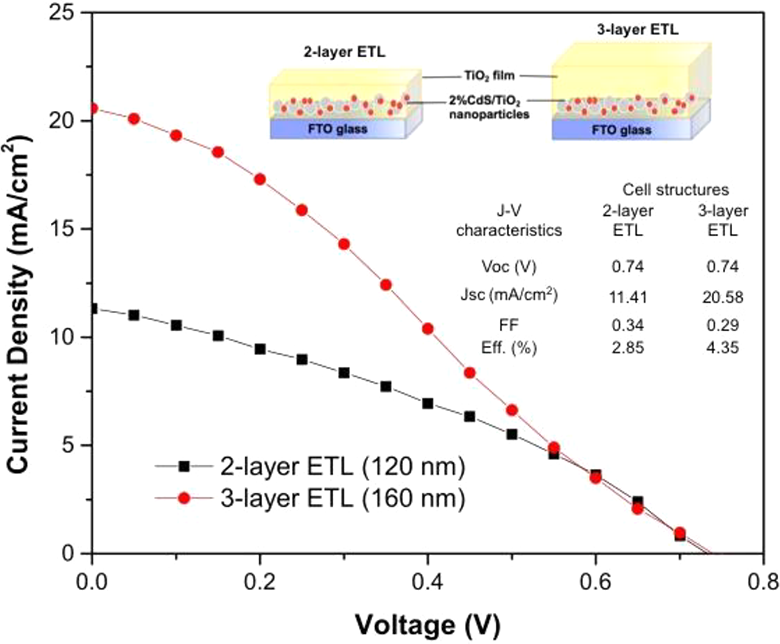
J-V curves of perovskite photovoltaic devices with two and three layers of ETLs (the first layer is 2% CdS/TiO2 nanoparticles). TiO2: titanium dioxide; CdS: cadmium sulfide; ETL: electron-transporting layer.
Conclusions
TiO2 nanoparticles modified by CdS QDs at various concentrations were synthesized by sol-hydrothermal method. The addition of CdS onto TiO2 nanoparticles mainly enhanced both optical absorption and electron transfer, as confirmed by UV-vis and PL spectra, respectively. The XRD patterns and morphologies of CdS QDs modified TiO2 nanoparticles were also demonstrated. Planar perovskite solar cells with various ETLs (i.e. TiO2 film, TiO2 nanoparticles, and CdS QDs-modified TiO2 nanoparticles) were prepared with the configuration of FTO/ETL/CH3NH3PbI3/spiro-OMeTAD/Ag. Under N2 atmosphere, a champion PCE of 8.16% was obtained from the cells made of TiO2 as the ETL. To study the potential for fabrication of perovskite solar cells for practical scales, the reference cells with TiO2 ETL were fabricated under an ambient atmosphere with RH approximately 50%. It was found that the PCE of the cell dramatically reduced to 1.33% (about 84% reduction), because the open-air atmosphere contains moisture and oxygen, causing the degradation of perovskite absorber films. With modification of TiO2 by CdS QDs, it was investigated that CdS can significantly enhance both J sc and PCE of the planar perovskite solar cells because it could enhance the charge transports. With variation of the concentrations of CdS doped on TiO2 nanoparticles, not only a changeable energy bandgap was presented but the optimum efficiency of the solar cells (2.40% from the cell made of 2%CdS QDs doped TiO2 nanoparticles) was also achieved, compared with the conventional cell made of only TiO2. The relative energy alignment of the cells with CdS is the key factor for the improvement of photovoltaic performance.
Supplemental material
Supplemental Material, 2020-07-07_Supplementary_Materials - Quantum dot-modified titanium dioxide nanoparticles as an energy-band tunable electron-transporting layer for open air-fabricated planar perovskite solar cells
Supplemental Material, 2020-07-07_Supplementary_Materials for Quantum dot-modified titanium dioxide nanoparticles as an energy-band tunable electron-transporting layer for open air-fabricated planar perovskite solar cells by Kanyanee Sanglee, Surawut Chuangchote, Taweewat Krajangsang, Jaran Sritharathikhun, Kobsak Sriprapha and Takashi Sagawa in Nanomaterials and Nanotechnology
Footnotes
Acknowledgments
The author KS would like to acknowledge Petchra Pra Jom Klao Doctoral scholarship of King Mongkut’s University of Technology Thonburi (KMUTT), Thailand. The Thailand Research Fund (TRF) (project RSA6180085) and Energy Policy and Planning Office (EPPO) (contract #801/2560), Ministry of Energy, partly supported this work. The authors thank other members of individual groups (KMUTT, National Science and Technology Development Agency (NSTDA) and Kyoto University for continuous support. In particular, we acknowledge the Department of Tool and Materials Engineering, KMUTT; Research Center of Advanced Materials for Energy and Environmental Technology (MEET), KMUTT; and Solar Energy Technology Laboratory (STL), NSTDA, for laboratory facilities.
Declaration of conflicting interests
The author(s) declared no potential conflicts of interest with respect to the research, authorship, and/or publication of this article.
Funding
The author(s) disclosed receipt of the following financial support for the research, authorship, and/or publication of this article: This research was financial supported by Energy Policy and Planning Office (EPPO) (contract #801/2560) and Thailand Science Research and Innovation (TSRI) (project RSA6180085) (Mid-Career Research Grant 2020 from National Research Council of Thailand).
Supplemental material
Supplemental material for this article is available online.
References
Supplementary Material
Please find the following supplemental material available below.
For Open Access articles published under a Creative Commons License, all supplemental material carries the same license as the article it is associated with.
For non-Open Access articles published, all supplemental material carries a non-exclusive license, and permission requests for re-use of supplemental material or any part of supplemental material shall be sent directly to the copyright owner as specified in the copyright notice associated with the article.