
Abstract
The research focuses on the applicability of silver (Ag) and molybdenum disulfide (MOS2) nanoparticle synthesized in situ in dimethylformamide solution as dielectric material for micro-electro discharge machining. Ag nanoparticles (~120 nm size) and MOS2 nanoparticles (~20 nm size) were synthesized in dimethylformamide solution using a combination of nanoparticle solution synthesis routes. A setup for micro-electro discharge machining was developed in-house with an arrangement to generate spark at varying voltages. The setup was integrated with a precise linear height gauge to measure the spark gap during the experiments where Ag and MOS2 nanoparticles in dimethylformamide solution served as dielectric. The debris was collected and was characterized for each of the experiments. The feature size of the crater generated during the micro-electro discharge machining was also studied. The experiments were repeated with silver and MOS2 nanoparticle powder mixed with dimethylformamide as dielectric. It was observed that in situ prepared nanoparticles in dimethylformamide offered much better machining performance in terms of process stability, crater size and material removal rates. On use of in situ synthesized nanoparticle dielectric, the material removal rate increased by nearly two to three times whereas the spark gap increased by about two times.
Keywords
Introduction
Powder-mixed dielectric for micro-electro discharge machining (EDM) is gaining significant popularity in research of late due to its large number of advantages such as high material removal rate (MRR), enhanced spark gap, higher process stability and better shape of machined features.1,2 In powder-mixed micro-EDM, electrically conductive powder is mixed and well dispersed in the dielectric of micro-EDM, which reduces the insulating strength of the dielectric fluid and increases the spark gap between the tool and the workpiece. As a result, the process becomes more stable thereby improving the MRR and surface roughness.3,4 The performance of such powder-mixed dielectric depends on factors such as powder size, conductivity of the powder and uniformity with which the powder is mixed with the dielectric. Although size and conductivity of the power-mixed fluid can be controlled easily, the uniformity while mixing is difficult to be assured as the physics behind mixing of a solid powder with a fluid can be of varying nature such as solid suspension and solid deagglomeration. 5
To ensure the uniformity of the mixed powder in the dielectric during EDM process, several researchers have proposed methods to impose external energy to the powder–dielectric mixture. Few of them include use of ultrasonic bath during EDM process,6,7 use of external stirrer for maintaining uniformity of the dielectric 8 and so on. Although such methods were found to be effective to disperse the powder uniformly in the solution, they require continuous source of external energy which is region-specific to the powder-mixed dielectric and depends on the location of energy source. Furthermore, the mixed powder particles settle down rapidly as a result of agglomeration of the dispersed particles due to lack of capping (stabilizing) agent in the powder particles. 9
To alleviate these issues, we propose a new technique of in situ nanoparticle (NP)-synthesized dielectric for micro-EDM in which NPs of less than 150 nm size are prepared in dimethylformamide (DMF) as solvent using standard NP synthesis routes. To universalize the process, we selected metallic (silver) NPs and semiconducting (MOS2) NPs synthesized in DMF as dielectric medium for micro-EDM. The performance measures of synthesized NP in situ in DMF are compared with NP powder mixed in DMF as dielectric for micro-EDM in terms of spark gap, debris formed, amount of material removed and size of crater.
Materials and methods
Dielectric synthesis and characterization
We used DMF as the solvent for preparation of Ag and MOS2-NP-based dielectric as it is simple to synthesize NPs in situ in DMF using regular synthesis routes. 10 Briefly, for synthesis of Ag-NPs, 20 mg polyvinylpyrrolidone (PVP) as capping agent was mixed in 40 mL DMF. The mixture was heated at 150°°C for 5 min with continuous stirring. About 10 mg AgNO3 and 5 mg NaBH4 were mixed with the solution. The entire mixture was stirred magnetically at 1240 r/min for 24 h. The resultant brownish colored solution was subjected to ultrasonication for 1 h at 70°°C and the solution was filtered using grade-4 filter paper. The solution was subjected to centrifugation at 9000 r/min for 15 min and the supernatant was separated. The supernatant served as the solution containing silver NPs. 11
Synthesis of MOS2-NPs was conducted by mixing and ultrasonication of 20 mg MOS2 powder with 40 mL DMF containing 10 mg PVP using a probe sonicator for 1 h followed by centrifugation of yellowish black mixture at 7000 r/min for 10 min. The supernatant hosted MOS2-NPs synthesized in situ in DMF solution.
Synthesis of Ag nanopowder- and MOS2 nanopowder-mixed DMF (dielectric) was conducted by mixing these commercially available nanopowders (silver nanopowder <150 nm particle size and MOS2 nanopowder ∼90 nm particle size from Sigma–Aldrich company) in DMF and continuous ultrasonication during experiments. The amount of nanopowders mixed was controlled in a manner such that the density of nanopowder-mixed dielectric and the in situ NP-synthesized dielectric is equal. Accordingly, 0.12 mg Ag nanopowder and 0.6 mg MOS2 were mixed in DMF for preparation of powder-mixed dielectric.
The in situ synthesized NP dielectric was characterized using field emission scanning electron microscope (FESEM). The NP solutions were also characterized using NP analyzer (NanoSight NS500). The factor-based increase/decrease in dielectric constant of in situ synthesized Ag and MOS2-NP dielectric and the powder-mixed dielectric over DMF solution was evaluated using cyclic voltammetry (CV) using PARSTAT 4000A potentiostat. A standard test cell with platinum working electrode, Ag/AgCl reference electrode and glassy carbon counter electrode were used for CV setup. The capacitance of each of the dielectric was calculated using equation (1) 12
where iavg is the average value of maximum current sweep magnitude in the CV curve, s is the scan rate and C is the capacitance measured.
The relative change in dielectric constant for the NP/nanopowder dielectric over DMF solution was assessed using equation (2)
where Cr is the measured capacitance of the reference sample (DMF), Cm is the measured capacitance of the nanopowder/NP containing dielectric and εt is the factor by which the dielectric constant of the nanopowder/NP containing dielectric is higher/lower than DMF.
Experiments for micro-EDM
A setup for micro-EDM was developed in-house which comprised a micro-EDM tool, a container for housing the liquid dielectric, the workpiece, a spark generation circuit and a linear height gauge for measurement of spark gap. The linear height gauge was fixed with a linear translation stage which can move along the Z-axis thus moving the tool up or down. The micro-EDM tool was fixed on the linear translation stage. The tool and the workpiece were connected to an electrical continuity testing instrument (multimeter). The experimental setup and the spark generation circuit are shown in Figure 1.
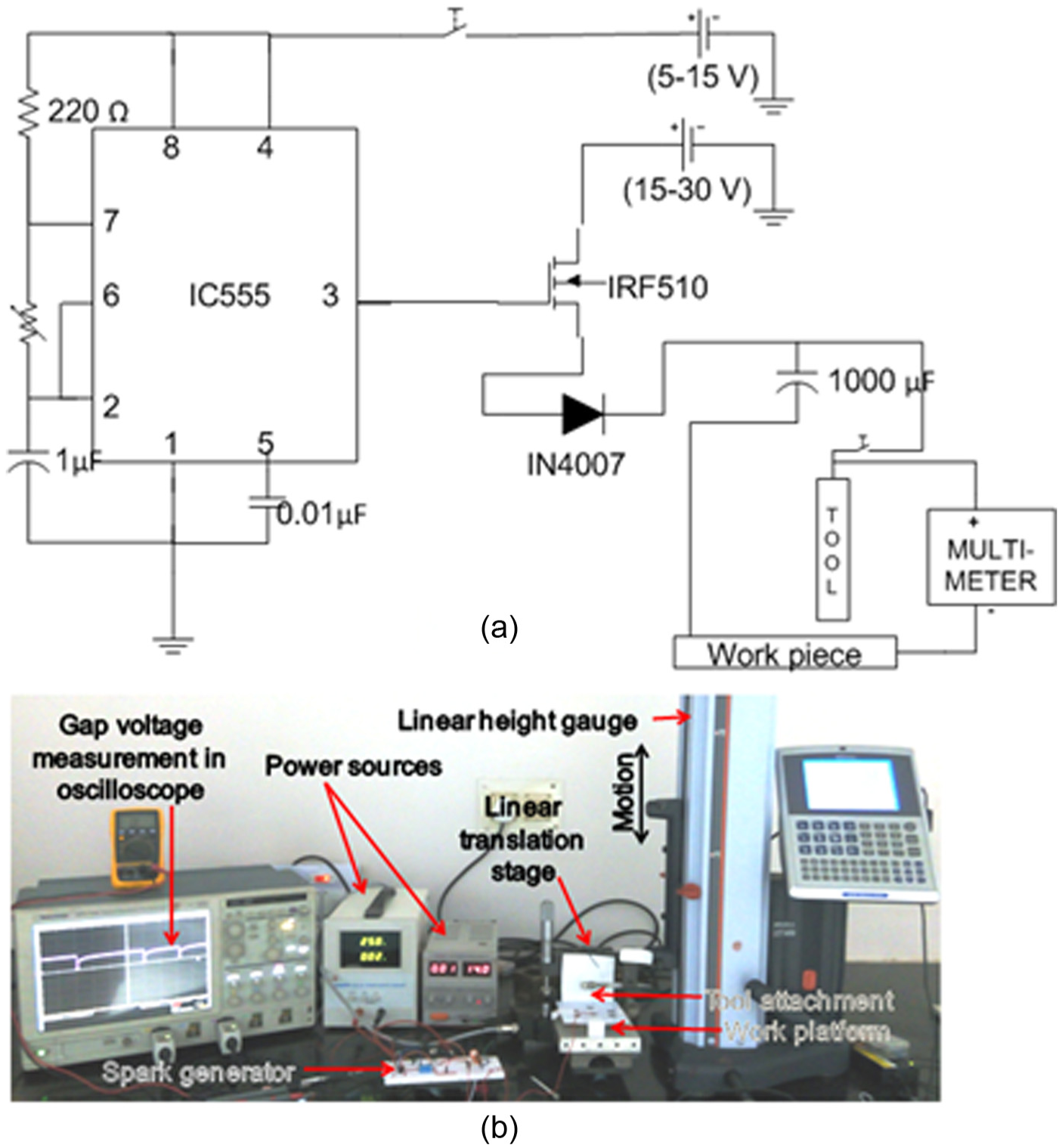
(a) Spark generator circuit used for micro-EDM experiments and (b) experimental setup for micro-EDM and measurement of spark gap.
Micro-EDM was conducted on Aluminum-6061 at three different spark gap voltages, namely, 20, 25 and 30 V for DMF, in situ synthesized MOS2-NP in DMF, in situ synthesized Ag-NP in DMF, powder-mixed MOS2-NP in DMF and powder-mixed Ag-NP in DMF as dielectric. For generation of spark and measurement of spark gap, the Z-axis stage was lowered so that the tool attached to it touched the work. The tool–workpiece touch was confirmed using continuity test, and the reading on the height gauge was recorded. The tool was again retraced back, and the spark generator circuit was activated. The tool was lowered slowly, and the spark occurring at a certain height was identified by a pop sound. The height gauge reading was again recorded at the moment the pop sound occurred. The difference between height gauge reading at tool–workpiece touch point and spark point rendered the spark gap length.
After each experiment, the dielectric fluid was collected separately. The fluid was centrifuged at 7000 r/min which led to settlement of the debris out from the dielectric solution. The debris was dried and was characterized using FESEM. Furthermore, the experiments were repeated for 50 times (50 sparks) to collect measurable amount of debris. The weight of debris obtained from 50 sparks at each gap voltage for each dielectric was measured using a precise balance. The micro-machined samples with single spark were analyzed for their crater size using FESEM.
Experimental results
The CV plots for DMF, in situ synthesized MOS2-NP in DMF, in situ synthesized Ag-NP in DMF, powder-mixed MOS2-NP in DMF and powder-mixed Ag-NP in DMF are shown in Figure 2.
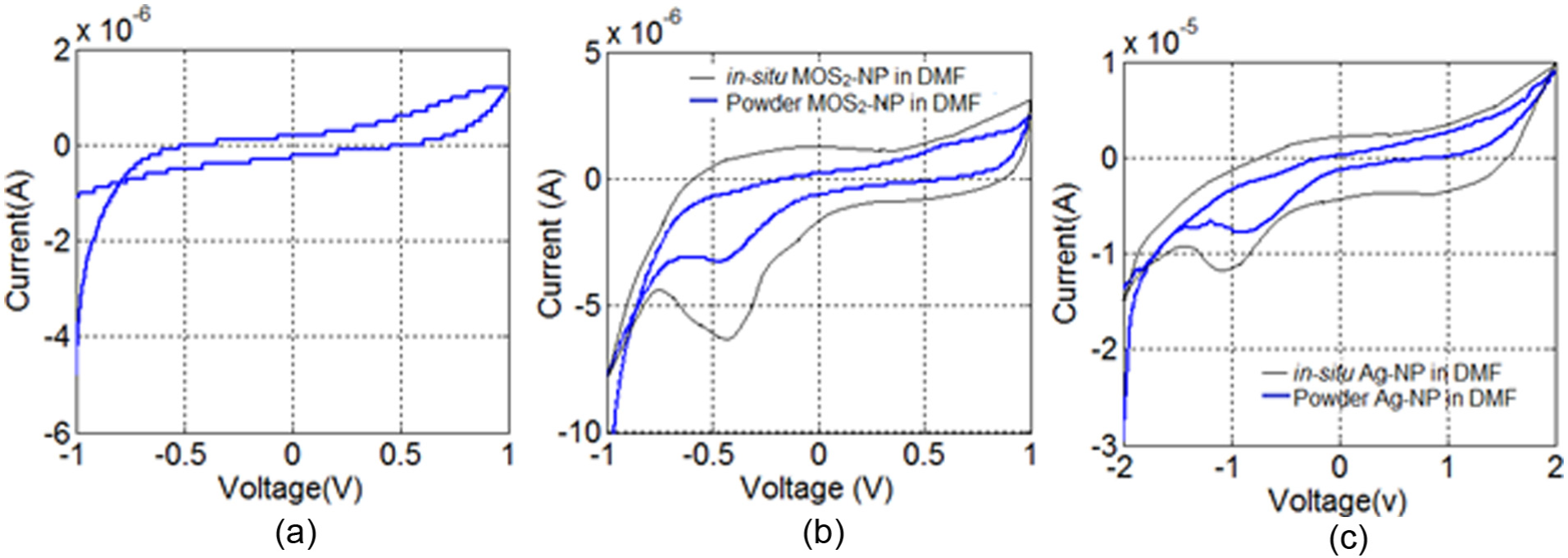
Cyclic voltammetry plots for (a) DMF, (b) in situ synthesized MOS2-NP in DMF and powder-mixed MOS2-NP in DMF and (c) in situ synthesized Ag-NP in DMF and powder-mixed Ag-NP in DMF.
The relative changes in dielectric constant of the materials with reference to DMF were calculated using equations (1) and (2). The dielectric constant of powder-mixed Ag-NP dielectric in DMF, in situ synthesized Ag-NP dielectric in DMF, powder-mixed MOS2 dielectric in DMF, in situ synthesized MOS2 dielectric in DMF were 6.57, 14.47, 4.07 and 9.47 times higher than DMF, respectively.
The FESEM images of in situ synthesized MOS2-NP in DMF and in situ synthesized Ag-NP in DMF are shown in Figure 3.
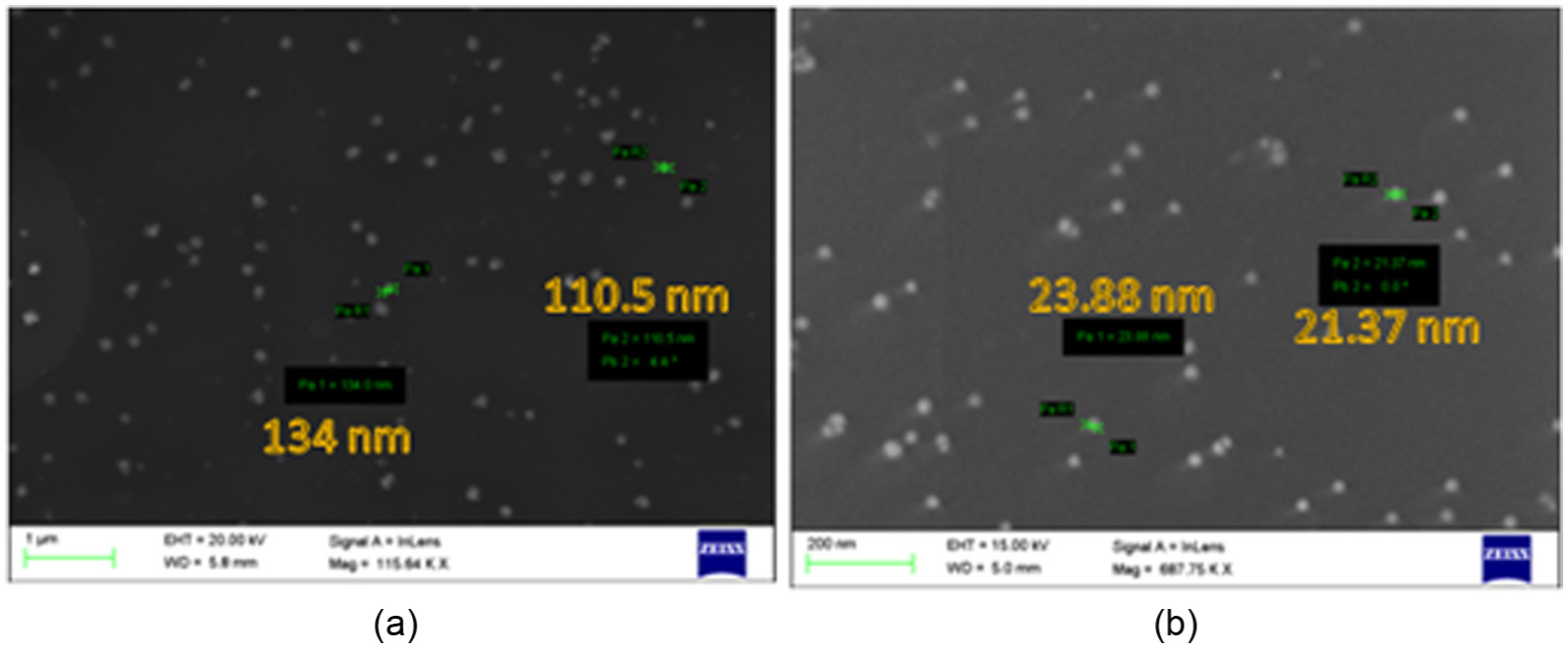
FESEM image of the in situ synthesized: (a) Ag-NP in DMF and (b) MOS2-NP in DMF.
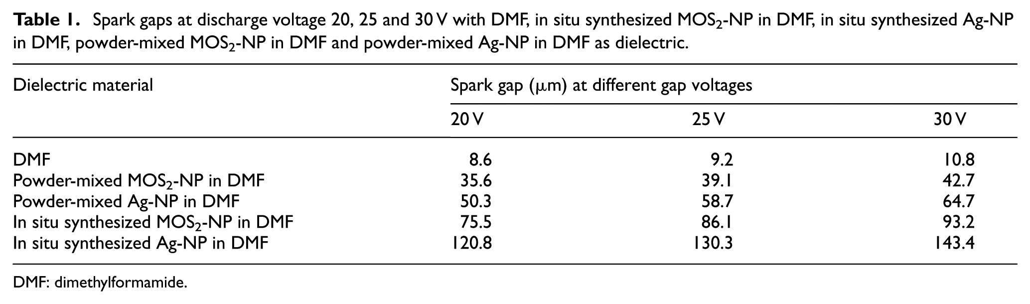
The NP solutions were also characterized using NP analyzer (NanoSight NS500) where the size of Ag-NP was found to be 120 nm and the size of MOS2-NP was 20 nm. The spark gap obtained during micro-EDM process at 20, 25 and 30 V discharge voltage with DMF, in situ synthesized MOS2-NP in DMF, in situ synthesized Ag-NP in DMF, powder-mixed MOS2-NP in DMF and powder-mixed Ag-NP in DMF as dielectric are shown in Table 1.
Spark gaps at discharge voltage 20, 25 and 30 V with DMF, in situ synthesized MOS2-NP in DMF, in situ synthesized Ag-NP in DMF, powder-mixed MOS2-NP in DMF and powder-mixed Ag-NP in DMF as dielectric.
DMF: dimethylformamide.
The FESEM images of debris collected after each experiment for spark gap voltage of 25 V are shown in Figure 4.
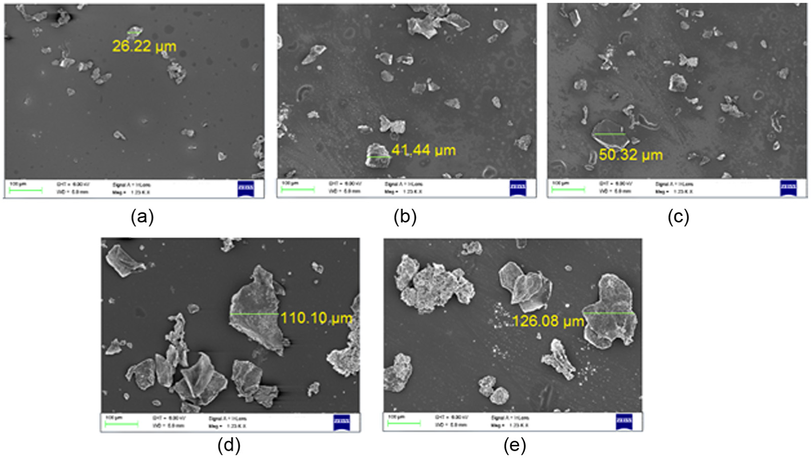
FESEM images of debris generated during the experiments with dielectric: (a) DMF, (b) powder-mixed Ag-NP in DMF, (c) powder-mixed MOS2 in DMF, (d) in situ synthesized MOS2 in DMF and (e) in situ synthesized Ag-NP in DMF.
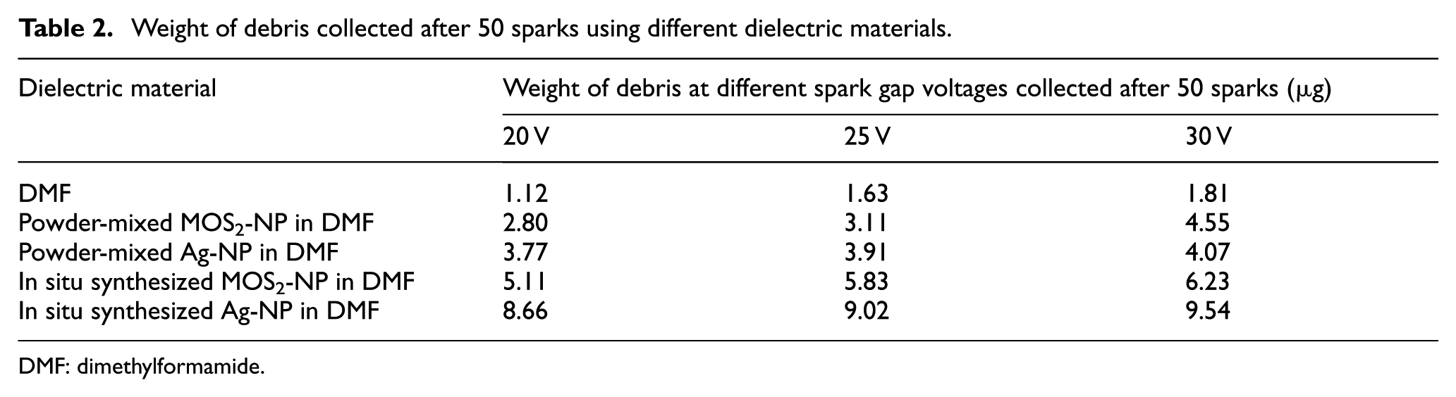
The weight of the debris generated for 50 sparks at three different gap voltages with different dielectric materials is shown in Table 2.
Weight of debris collected after 50 sparks using different dielectric materials.
DMF: dimethylformamide.
The crater morphology as found using FESEM at spark gap voltage 25 V is shown in Figure 5.
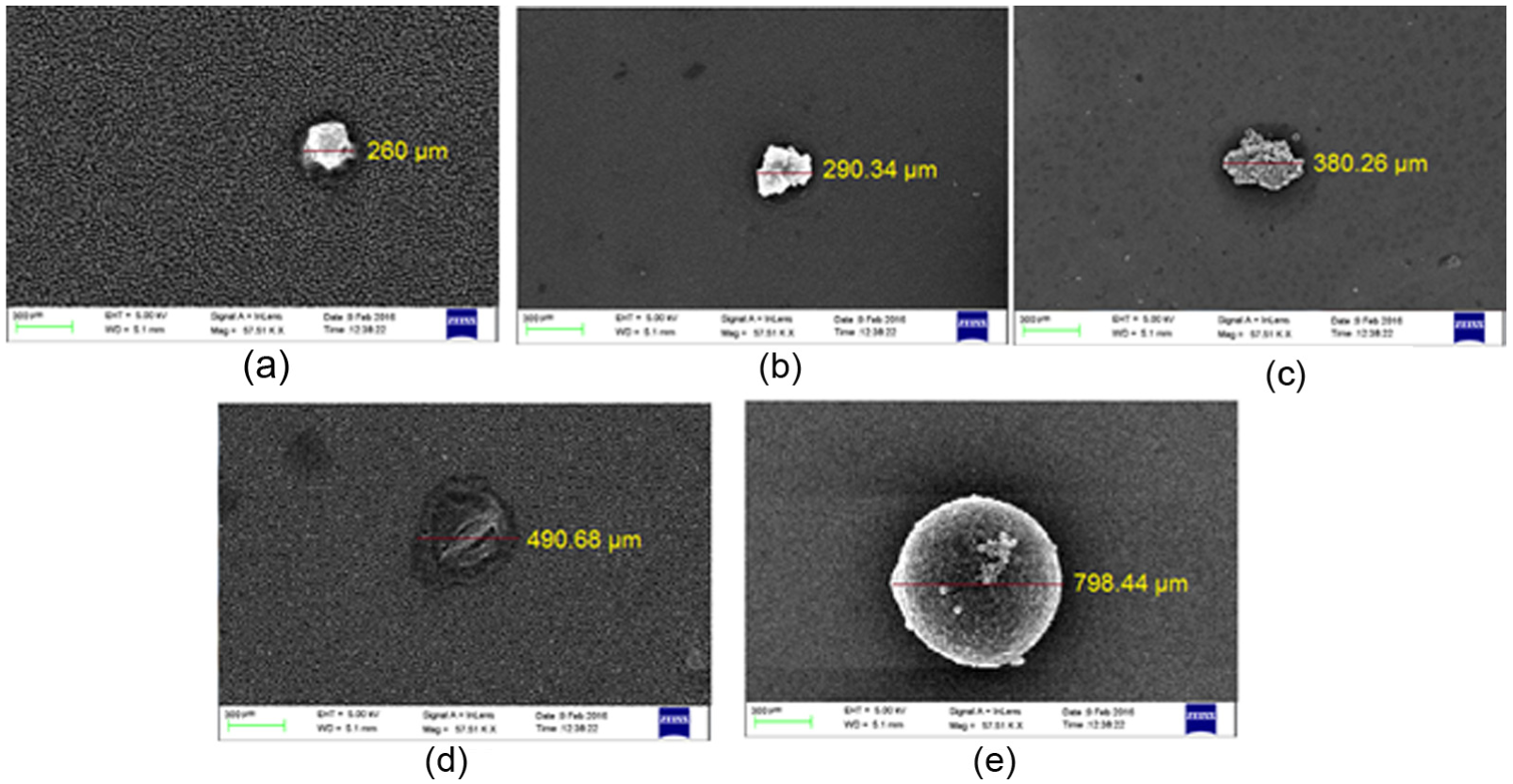
FESEM images of machined craters with dielectric: (a) DMF, (b) powder-mixed Ag-NP in DMF, (c) powder-mixed MOS2 in DMF, (d) in situ synthesized MOS2 in DMF and (e) in situ synthesized Ag-NP in DMF.
The following could be inferred from the experimental results:
The use of in situ NP-synthesized dielectric renders better micro-EDM results as compared to nanopowder-mixed dielectric in terms of process stability. The spark gap while using in situ NP-synthesized dielectric increases twofold as compared to nanopowder-mixed dielectric (Table 1). This might be due to better stability and lack of agglomeration of NPs in solution due to use of stabilizing agent for in situ NP-synthesized dielectric.
The increase in spark gap can be justified from Figure 1 and the dielectric constants of in situ synthesized NP dielectric and -mixed dielectric. As stated earlier, the dielectric constant of powder-mixed Ag-NP dielectric in DMF, in situ synthesized Ag-NP dielectric in DMF, powder-mixed MOS2 dielectric in DMF and in situ synthesized MOS2 dielectric in DMF were 6.57, 14.47, 4.07 and 9.47 times higher than DMF, respectively. The spark gap for powder-mixed Ag-NP dielectric in DMF, in situ synthesized Ag-NP dielectric in DMF, powder-mixed MOS2 dielectric in DMF and in situ synthesized MOS2 dielectric in DMF also increased by approximately similar factors (Table 1). This shows that there is a direct correlation between the dielectric constant of the dielectric and spark gap length.
The FESEM images of the debris as shown in Figure 4 show that the debris generated while using powder-mixed dielectric were smaller and without any agglomeration, whereas the debris generated while using in situ nanopowder-based dielectric were larger and shows agglomeration. This indicates the fact that in micro-EDM process, in situ synthesized dielectric leads to higher spark gap energy as compared to nanopowder-mixed dielectric. The higher energy may be due to higher dielectric constant (better polarizability) of in situ synthesized dielectric as compared to nanopowder-mixed dielectric.
The weight of debris on use of in situ NP-synthesized dielectric increased two- to threefold than powder-mixed dielectric (Figure 4). This confirms the fact that use of in situ NP-synthesized dielectric renders higher MRR in micro-EDM process than powder-mixed dielectric.
The higher MRR can also be confirmed from Figure 5 wherein the size of machined crater was higher on use of in situ NP-synthesized dielectric. Furthermore, on use of in situ NP-synthesized dielectric, uniform circular crater structure could be found which indicates uniform distribution of energy in the spark gap. This is due to better and uniform distribution of the NPs in situ NP-synthesized dielectric as compared to nanopowder-mixed dielectric.
Conclusion
The use of powder-mixed dielectric for improvement of machining parameters for micro-EDM is an emerging area of research. In this work, a modification of the powder-mixed EDM process was conducted wherein NPs were synthesized in situ in a dielectric media (DMF) instead of continuous mixing and stirring of the powder with the dielectric. The results and inferences indicated that use of in situ synthesized NP dielectric in micro-EDM process enhances the MRR by two to three times and spark gap by two times while maintaining uniformity in distribution of spark gap energy. Moreover, increase in spark gap enhances the stability of micro-EDM process by eliminating unnecessary arcing phenomenon. Additionally, higher and uniform spark gap energy leads to higher MRR and better shape of the machined features. The process is particularly beneficial for machining industries where process stability and enhancement of MRR in micro-EDM is a major concern. The process also bears benefits in terms of energy conservation as external stirring or energy needs not to be applied continuously to the dielectric.
Footnotes
Declaration of conflicting interests
The author(s) declared no potential conflicts of interest with respect to the research, authorship and/or publication of this article.
Funding
The author(s) received no financial support for the research, authorship and/or publication of this article.