
Abstract
Surface textures, especially micro-dimple arrays, can significantly improve the friction performance of engineering parts. Through-mask electrochemical micromachining is an effective method for generating micro-dimple arrays. In this article, a new method is introduced to fabricate a large-area polydimethylsiloxane mask containing micro through-holes. Using this technique, a stainless steel mould with micro-pillar arrays is generated by wire electrical discharge machining. A combination of pressure and weight of electrolyte is then proposed to keep the polydimethylsiloxane mask closely attached to the workpiece, which helps to achieve high machining accuracy. The effects of applied voltage, effective machining time and pulse duty cycle on the micro-dimples are investigated. The profiles of the micro-dimples are not sensitive to applied voltage, but pulse duty cycle is a significant factor influencing the depth of the micro-dimples. Micro-dimples of width 95 µm, depth 19 µm and a machining area of diameter 40 mm are successfully generated using a polydimethylsiloxane mask, and the standard deviations of the micro-dimple width and depth are only 0.84 and 0.23 µm, respectively. The present experiments verify that it is feasible to obtain large-area micro-dimple arrays with high machining accuracy using this technique.
Keywords
Introduction
In recent years, surface texturing technology has proven to be a suitable method for improving the friction performance of engineering parts. Possible surface textures include micro-dimples, micro-prisms, micro-grooves and micro-pillars; among these, micro-dimple arrays are widely used because of their excellent tribological properties. Micro-dimple arrays can reduce friction and wear on automobile engine pistons, improve lubrication sealing properties and enhance energy efficiency.1,2 Using surface textures can preserve lubricating oil and enhance the retention of a lubricating thin film to improve lubrication between components. 3 It has been observed that compared to a flat, smooth surface, it is feasible for a surface with micro-dimple arrays to reduce friction by more than 30%. 4 Moreover, using surface textures on a cutting tool for difficult-to-machine materials can increase tool lifetime, as it can enhance the tribological properties of the tool. 5 It has also been proved that compared to smooth surfaces, textured surfaces can enhance evaporation efficiency in spray cooling. 6
A number of methods have been used to generate micro-dimple arrays: micro-milling, 7 electrical discharge machining, 8 laser beam machining, 9 abrasive jet machining 10 and electrochemical machining (ECM).11,12 Among these, ECM is a popular method because of the advantages of being unaffected by material hardness and toughness, the lack of a heat-affected layer and residual stresses, the absence of tool wear and high efficiency for large-area machining. Natsu et al. 13 fabricated micro-dimples 20 µm in depth on a plate and a cylindrical surface by electrolyte jet machining. The workpiece material exposed to the jet, which was ejected from the cathodic nozzle, was removed due to electrochemical dissolution. Wang et al. 14 fabricated micro-dimples with a diameter of 440 µm by electrochemical micro-drilling using a tool electrode. However, the efficiency of machining large areas was poor because the micro-dimples were generated individually. Park and Chu 15 fabricated micro-dimple arrays with multiple tool electrodes. Schonenberger and Roy 16 proposed a method for transferring micro-scale patterns without photolithography of substrates. In this method, the cathode was covered with a resist pattern and the anode was fully exposed. Square dimples of width 120 µm and depth 1.5 µm were fabricated on a copper disc of diameter 1 cm, with a low localization of the removal area.
In recent years, through-mask electrochemical micromachining (TMEMM) has been an effective method for generating micro-dimple arrays. Using this technology, all the micro-dimples can be generated at the same time, and their size, location and density can be controlled. In conventional TMEMM, a mask with through-holes is prepared by photolithography using photoresist, following the procedures of spin coating, prebaking, exposure, development and postbaking. The workpiece is covered with an insulated mask containing through-holes. When the electrolyte flows into a through-hole, a micro-dimple at the exposed region is generated by electrochemical dissolution. Using this method, Madore and Landolt 17 fabricated micro-hemispherical cavities with a diameter of 30 µm on titanium, but the machining surface area was only 1 cm2. Yan et al. 18 fabricated micro-dimple arrays with a diameter of 50 µm and a depth of 20 µm on a ring. However, it is complicated to generate micro-dimple arrays using photoresist, because the photoresist needs to be removed after ECM, and it is expensive for mass production. In addition, it is difficult to obtain a large area of patterned mask because of the limitations of photolithography, which therefore limits the application of micro-dimple arrays on the surfaces of engineering parts. Qu et al. 19 used a dry-film photoresist as a mask for the production of micro-dimple arrays on a cylindrical inner surface. The dry-film photoresist was attached to the workpiece after exposure and development. However, the dry-film photoresist could only be used once.
Polydimethylsiloxane (PDMS) is widely used in many applications because of its chemical resistance, high flexibility and high moulding capability. Chen and colleagues20,21 developed a new method for fabricating a PDMS mask with micro through-holes to generate micro-dimple arrays, with the advantage that it has a high localization of machining area. In this method, a mould (fabricated out of SU-8 photoresist) with micro-pillar arrays was filled with PDMS gel. A PDMS mask was obtained when the PDMS gel solidified. The PDMS mask thus generated is reusable; however, the SU-8 mould is disposable and a large-area PDMS mask with micro through-holes is difficult to prepare because the SU-8 micro-pillar arrays easily fall off the substrate. In previous work, the maximum machining area of a PDMS mask, prepared using an SU-8 mould, has only had a diameter of 10 mm.22,23 Although large-area micro-dimple arrays are potentially useful in engineering applications, it is still a challenge to prepare sufficiently large-area PDMS mask with micro through-holes.
In this article, a method for fabricating a large-area PDMS mask with through-holes is presented. A stainless steel mould with micro-pillar arrays, generated by wire electrical discharge machining (WEDM), is used. A vacuum-aided process is used to fill the mould with the PDMS gel, and after solidification of the PDMS gel, the mask can be separated from the mould. The large-area PDMS mask with micro through-holes can be easily prepared by the presented method.
It is critical to achieve high machining accuracy by ensuring that the PDMS mask stays closely attached to the workpiece surface during ECM, which prevents the electrolyte from permeating into the interface between the PDMS mask and workpiece. However, it is hard to keep the PDMS mask closely attached to the workpiece surface, especially for a large-area PDMS mask. In this article, a combination of pressure and weight of electrolyte is used to keep the mask closely attached to the workpiece surface during ECM. The gap between the cathode and anode is 10 mm, and the weight of the electrolyte is helpful to keep the PDMS mask closely attached to the workpiece surface. Moreover, back pressure was also introduced so that a high hydraulic pressure was exerted on the PDMS mask to prevent the electrolyte from permeating into the interface between the PDMS mask and workpiece. The effects of applied voltage, machining time and pulse duty cycle on the micro-dimples are investigated. Micro-dimple arrays of width 95 µm and depth 18.9 µm can be generated on a disc of machining diameter 40 mm, with an effective machining time of 24 s.
Fabrication of a PDMS mask
Materials and methods
Stainless steel 304 with a polished surface was used to fabricate the PDMS mask. PDMS gel (Slygard 170; Dow Corning Corp., USA) was poured into the mould. A WEDM (Agiecut Challenge Ecut 2F; Agie, Switzerland) was used to fabricate the stainless steel mould. A scanning electron microscope (S3400N; Hitachi, Japan) and a three-dimensional profilometer (DVM500; Leica, Germany) were used to analyse the stainless steel mould, the PDMS mask and the micro-dimple arrays.
In this study, the fabrication of a PDMS mask with through-holes was divided into two steps: mould making and PDMS moulding, with mould making being the most important step.
Fabrication of a stainless steel mould
Figure 1 presents a schematic diagram of the fabrication process for a stainless steel mould. First, a plate of stainless steel 304 was mechanically polished. Second, micro-grooves on the polished surface were generated using WEDM with an electrode wire of diameter 0.1 mm fed transversely after generating a groove (Figure 1(b)). Third, micro-pillar arrays were generated by longitudinal WEDM (Figure 1(c)). The current was 13 A and pulse duty cycle was 80% during WEDM, and dielectric liquid was deionized water. The electrode wire was parallel to the polished surface and the micro-pillar arrays of the stainless steel mould were square. A stainless steel mould with micro-pillar arrays is shown in Figure 2. The width and height of the micro-pillar arrays were 85 and 240 µm, respectively, and a mould of width 50 mm and length 100 mm was fabricated.
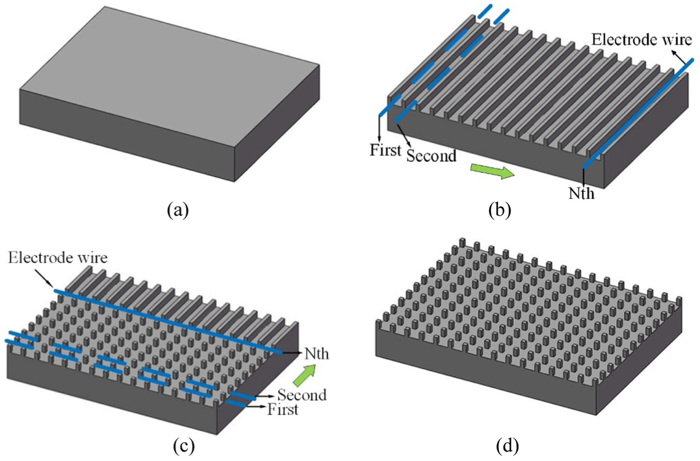
Fabrication process for a stainless steel mould with micro-pillar arrays: (a) polishing, (b) transverse WEDM, (c) longitudinal WEDM and (d) mould with micro-pillar arrays.
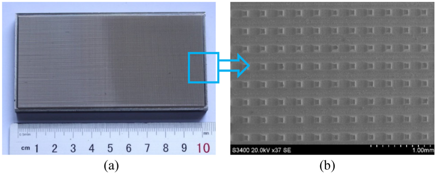
Stainless steel mould with micro-pillar arrays: (a) image of a mould and (b) scanning electron microscope image of micro-pillar arrays.
Fabrication of a through-hole PDMS mask
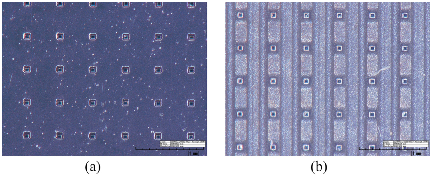
Details of the fabrication procedure of a PDMS mask using a mould have been described in our previous work. 20 Figure 3 presents a schematic diagram of the fabrication process for a through-hole PDMS mask. First, an adhesive tape was stuck onto the mould to form a semi-enclosed space. Second, the mould was put in a container and the micro-pillar arrays were filled with PDMS gel in a vacuum chamber. Third, the mould containing the PDMS gel was put into an oven at 70 °C for 30 min and the PDMS gel solidified. Finally, the through-hole PDMS mask was separated from the stainless steel mould and adhesive tape. A fabricated through-hole PDMS mask is shown in Figure 4. One side of the PDMS mask is smooth (Figure 4(a)), and the other side is rough (Figure 4(b)). The smooth side corresponds to the adhesive tape on the polished surface. There are grooves in the rough side because the bottom of the mould was machined by WEDM. A PDMS mask with through-holes of width 85 µm and thickness 240 µm was fabricated. The through-holes of the PDMS mask were square and the micro-dimples generated by the PDMS mask were therefore also square. Yu et al. 24 reported that compared to circular dimples, square dimples have a better friction reduction effect.
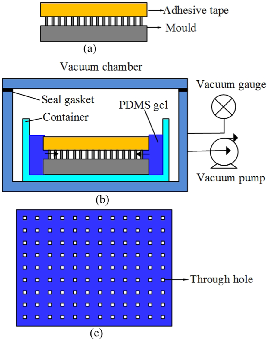
Fabrication process for a PDMS mask: (a) adhesive tape stuck onto the mould, (b) micro-pillar arrays filled with PDMS gel and (c) solidified PDMS mask separated from the mould.
Fabricated PDMS through-hole mask: (a) smooth side and (b) rough side of a PDMS mask.
ECM experiments
A PDMS mask with through-holes of width 85 µm and thickness 240 µm was used to generate micro-dimple arrays by TMEMM. The adhesion between the PDMS mask and workpiece is an important factor that influences the generation of micro-dimple arrays and helps to achieve high machining accuracy. Figure 5 presents a schematic diagram of ECM with the PDMS mask. A cathode with a multislit structure (shown in Figure 6) was designed to improve the uniformity of electrolyte flow, because the electrolyte flows through the slit structure and the electrolyte flow modes on the workpiece are the same. The multislit structure of slit width (L) 0.2 mm and a distance (L 0) between slits of 0.8 mm was generated using WEDM. An electrode wire passing through a through-hole was produced on the cathode, and then, a slit was generated by WEDM.
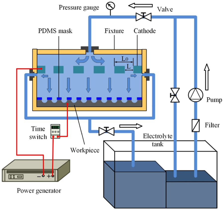
Schematic diagram of ECM with a PDMS mask.
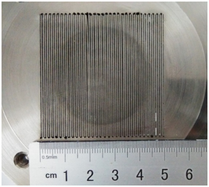
Image of a cathode with a multislit structure.
It has already been demonstrated that the proportionate distribution of an electric field over a workpiece does not alter with changing inter-electrode gap. 19 To prevent the electrolyte from permeating into the interface between the PDMS mask and workpiece, a combination of the pressure and weight of the electrolyte was used to keep the PDMS closely attached to the workpiece surface during ECM. The gap between the cathode and anode is 10 mm, and the liquid outlet is far from the workpiece, located on the surface of the cathode, so that the weight of the electrolyte will keep the PDMS mask closely attached to the workpiece surface; this is different from conventional TMEMM. Moreover, back pressure was also introduced so that a high hydraulic pressure was exerted on the PDMS mask to prevent the electrolyte from permeating into the interface between the PDMS mask and workpiece, which is essential for high machining accuracy.
The electrolyte was sodium nitrate (NaNO3) solution at a concentration of 100 g/L, a temperature of 25 °C and a pressure of 0.2 MPa. The workpiece was stainless steel 304 of diameter 50 mm, and a PDMS mask with a distance between through-holes of 500 µm was cut into a circle. The frequency of pulsed current was 120 Hz. Three groups of experiments with different machining parameters including applied voltage, effective machining time and pulse duty cycle were conducted. The effects of these parameters on the width and depth of the micro-dimples were investigated.
In this article, the effective machining time is the time of current pulse at a high level, and total machining time is all the cycles’ time of the pulsed current. When the effective machining time was t 0, the total times at different pulse duty cycles can be expressed as
Results and discussions
Effects of machining parameters on micro-dimple profiles
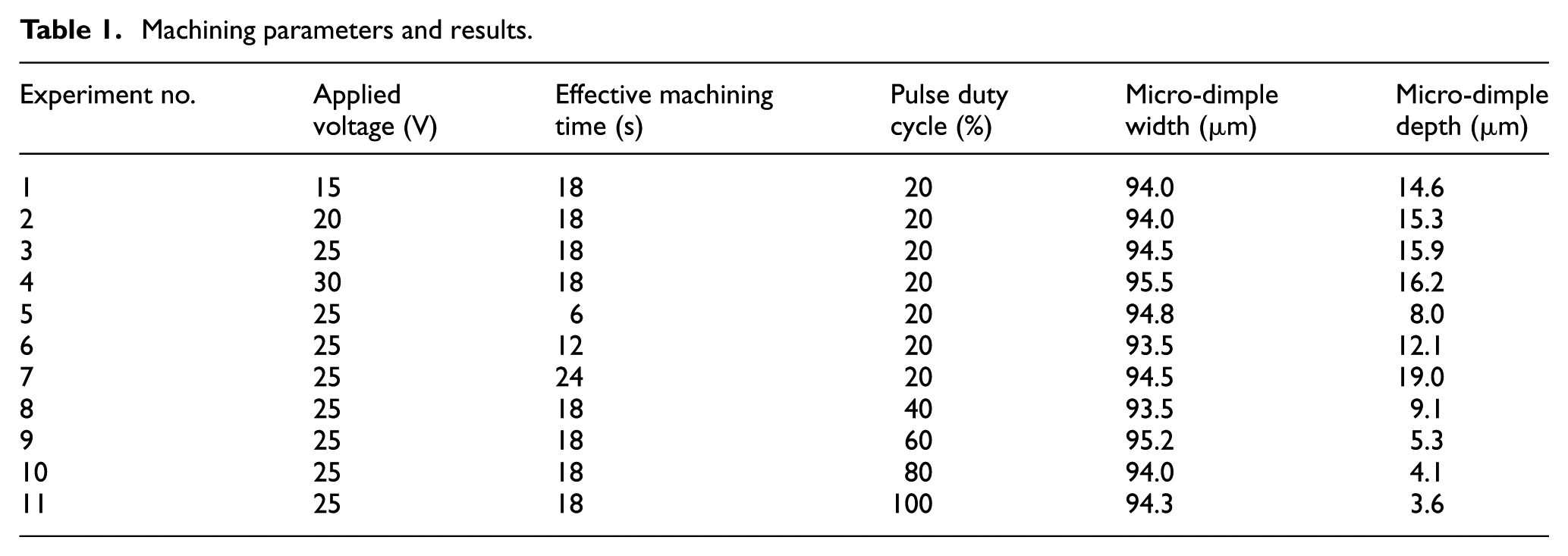
Applied voltage, effective machining time and pulse duty cycle were varied to investigate the effects of these parameters on the micro-dimples. The machining parameters and results are given in Table 1. Experiments 1–4 were performed to investigate the effects of applied voltage on the micro-dimples; experiments 3, 5, 6 and 7 were performed to investigate the effects of effective machining time on the micro-dimples; and experiments 3 and 8–11 were performed to investigate the effects of pulse duty cycle on the micro-dimples. The effects of applied voltage on the width and depth of micro-dimples at an effective time of 18 s are shown in Figure 7(a). As the applied voltage increased, the micro-dimple width ranged from 94 to 96 µm and the depth ranged from 14.5 to 16.2 µm. Generally, a higher current density should enlarge the profiles of dimples, so the width and depth of the micro-dimples increase as the applied voltage increases. Qu et al. 19 reported that using a dry-film photoresist mask with micro-holes of 50 µm diameter in TMEMM, as voltage increased, led to an increase in the diameter of the micro-dimples from 84 to 110 µm and an increase in the depth from 11.4 to 16.7 µm. In TMEMM, the distribution of electrical field on the workpiece was non-uniform because of the marginal effect of electrical field. 22 According to Faraday’s law, the non-uniform distribution of electrical field might lead to the non-uniform material removal rate (MMR) of micro-dimple arrays and a low machining accuracy. In contrast, with the method described here, the width and depth of the micro-dimples can be seen to increase over only a narrow range with increasing voltage. Therefore, the profiles of the micro-dimples are not sensitive to applied voltage, which weakens the effect of non-uniform distribution of electrical field on generating micro-dimple arrays. It can be concluded that this method can achieve a high machining accuracy with PDMS mask.
Machining parameters and results.
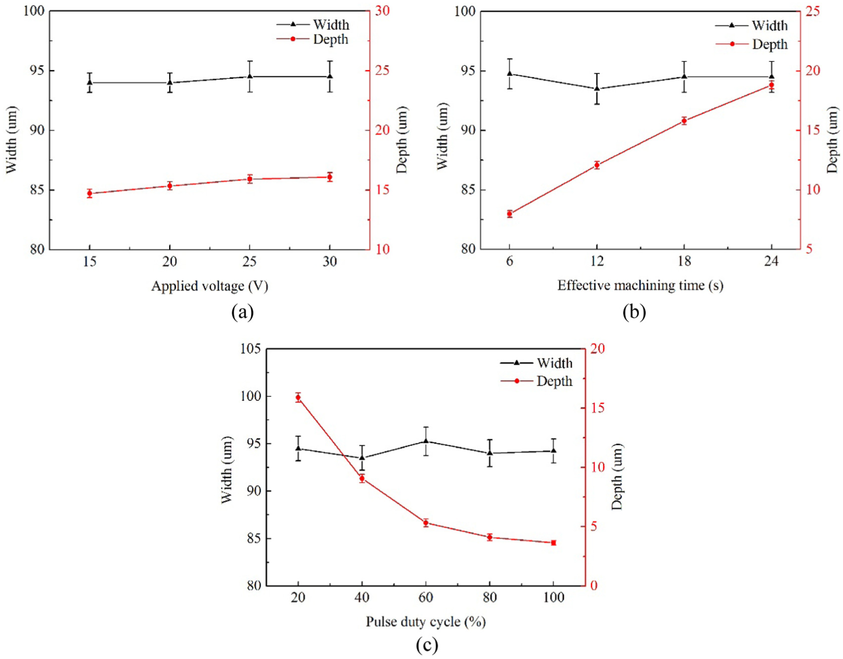
Effects of (a) applied voltage, (b) effective machining time and (c) pulse duty cycle on the width and depth of micro-dimples.
In this article, the workpiece is stainless steel 304 and the reactions at the electrodes could be described as follows
At the anode

At the cathode

where M represents the metal of workpiece. It has been observed that oxygen bubbles were produced in micro-dimples during the workpiece dissolving. 25
In this study, the aspect ratio of the through-holes is more than 2.8, which leads to the accumulation of the reaction products in the through-holes and micro-dimples because the escape of them slows down. As the applied voltage increases, the reaction products increase, which increases the inter-electrode resistance and weakens the increase in current. Thus, the profiles of the micro-dimples are not sensitive to applied voltage.
Figure 7(b) shows the effects of effective machining time on the width and depth of the micro-dimples. As the effective machining time increases, the width of the micro-dimples shows no obvious change, but the depth of the micro-dimples increases. The depth of the micro-dimples increased from 12.1 to 15.9 µm as the effective machining time increased from 12 to 18 s, while the depth became 19.0 µm at an effective machining time of 24 s . It was found that the increase in depth slowed with prolonged effective machining time. This is because, as the depth increases, the removal of the reaction products and replacement of electrolyte become increasingly more difficult.
Experiments 3 and 8–11 were performed to investigate the effects of pulse duty cycle on the micro-dimples. The effective machining time was 18 s and the total machining times at pulse duty cycle of 20%, 40%, 60%, 80% and 100% were 90, 45, 30, 22.5 and 18 s, respectively. Figure 7(c) shows that there is little change in the width of the micro-dimples. As the pulse duty cycle increases from 20% to 100%, the depth of the micro-dimples decreases rapidly at the same effective machining time, which indicates that the pulse duty cycle is a significant factor influencing the depths of the micro-dimples. This phenomenon can be attributed to the reaction products, especially the oxygen bubbles occurring in the micro-dimples. When the effective machining time is fixed, as the pulse duty cycle decreases, the relaxation time of zero current becomes longer, which is beneficial to the removal of reaction products and replacement of the electrolyte; hence, the current increases and the depth of the micro-dimples increases. The relation of pulse duty cycle and MRR or profile of the micro-features has been investigated. Rathod et al. 26 reported that the increase in MRR was slowed after 40% of pulse duty cycle. This indicates that at a higher pulse duty cycle, the profiles of grooves will decrease at same effective machining time. The depth of micro-dimple sharply reduced from 20 to 6.4 µm at an effective machining time of 15 s when the duty cycle increased from 20% to 80%. 23 Figure 8 shows scanning electron microscopic images and three-dimensional profiles of micro-dimple arrays with different pulse duty cycles. It can be concluded that both pulse current and direct current are capable of generating micro-dimple arrays with good profiles.
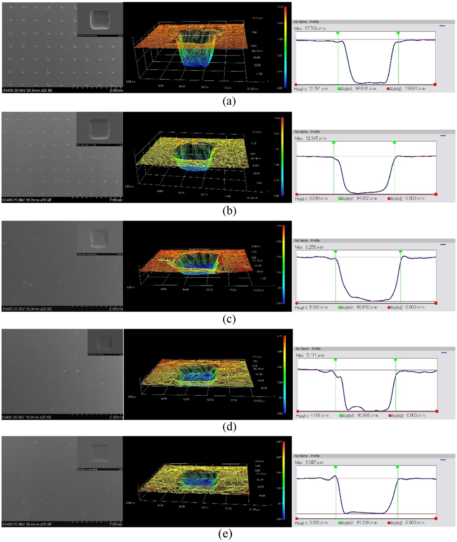
Scanning electron microscopic images and three-dimensional profiles of micro-dimple arrays generated with different pulse duty cycles: (a) 20%, (b) 40%, (c) 60%, (d) 80% and (e) 100% duty cycle.
It is difficult for oxygen bubbles to escape from the through-holes and micro-dimples because of the pressure and weight of the electrolyte. Hence, many oxygen bubbles accumulate on the inner surfaces of the micro-dimples and will slow down the dissolution rate of the workpiece, which helps to achieve a higher machining accuracy.
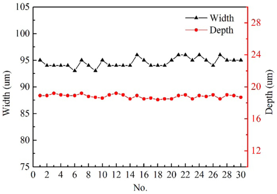
Machining accuracy of micro-dimple arrays generated with large-area PDMS mask
The uniformity of the micro-dimple arrays indicates the machining accuracy of micro-dimple arrays generated using a PDMS mask. To investigate the machining accuracy of the micro-dimple arrays, an experiment was performed with an applied voltage of 25 V, a pulse duty cycle of 20% and an effective machining time of 24 s. The width of the through-holes of the PDMS mask was 85 µm. Figure 9 shows an image of a workpiece with a round machining area of diameter 40 mm. A total of 30 observations were taken uniformly in the machining area, and the width and depth of the micro-dimples are shown in Figure 10. The standard deviations of micro-dimples’ width and depth are used to quantify the amount of dispersion of width and depth. They are correlated with the machining accuracy and can be calculated as follows 26
where SW is the standard deviation of the micro-dimple width, Wi is the micro-dimple width at the ith measurement, W is the average width of the micro-dimples, SH is the standard deviation of the micro-dimple depth, Hi is the micro-dimple depth at the ith measurement, H is the average depth of the micro-dimples and N is the total number of measured micro-dimples. SW and SH mean the spread of width and depth about average values. Lower values of SW and SH are preferred, and it signifies uniform micro-dimples and high machining accuracy.
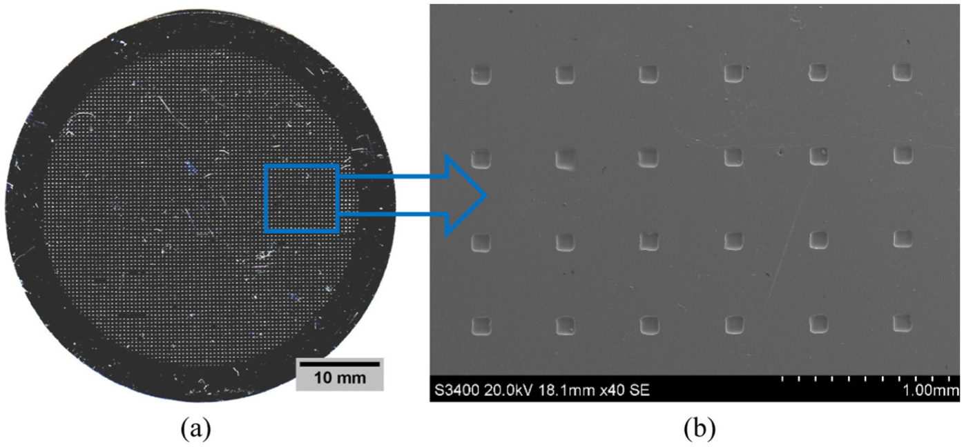
(a) Image of the workpiece with a round machining area and (b) a scanning electron microscopic image of the micro-dimple arrays.
Width and depth of micro-dimple arrays at different locations.
In this experiment, the average width and depth of micro-dimples were 94.6 and 18.8 µm, respectively. The width ranged from 93 to 96 µm, and the depth ranged from 18.4 to 19.2 µm. From equations (4) and (5), the standard deviations of the micro-dimple’s width and depth were only 0.84 and 0.23 µm, respectively. Zhang et al. 27 fabricated micro-dimples using a movable dry-film mask; when the diameter and depth of the micro-dimple arrays were 109.71 and 11.89 µm, respectively, the standard deviations of the micro-dimple’s diameter and depth were 2.018 and 1.287 µm, respectively. It can be concluded that in the present experiment, the width and depth of the micro-dimple arrays did not significantly change in different locations, and the machining accuracy of the micro-dimple arrays was high.
Figure 11 shows three-dimensional profiles of micro-dimple arrays at the edge, at half of the radius and at the centre of the machining area. As Figure 11 shows, the profiles of micro-dimples at different locations did not significantly change and the micro-dimples were square with uniform profiles. The micro-dimples are square because the through-holes of the PDMS mask are square, which gives a high machining accuracy in TMEMM with PDMS.
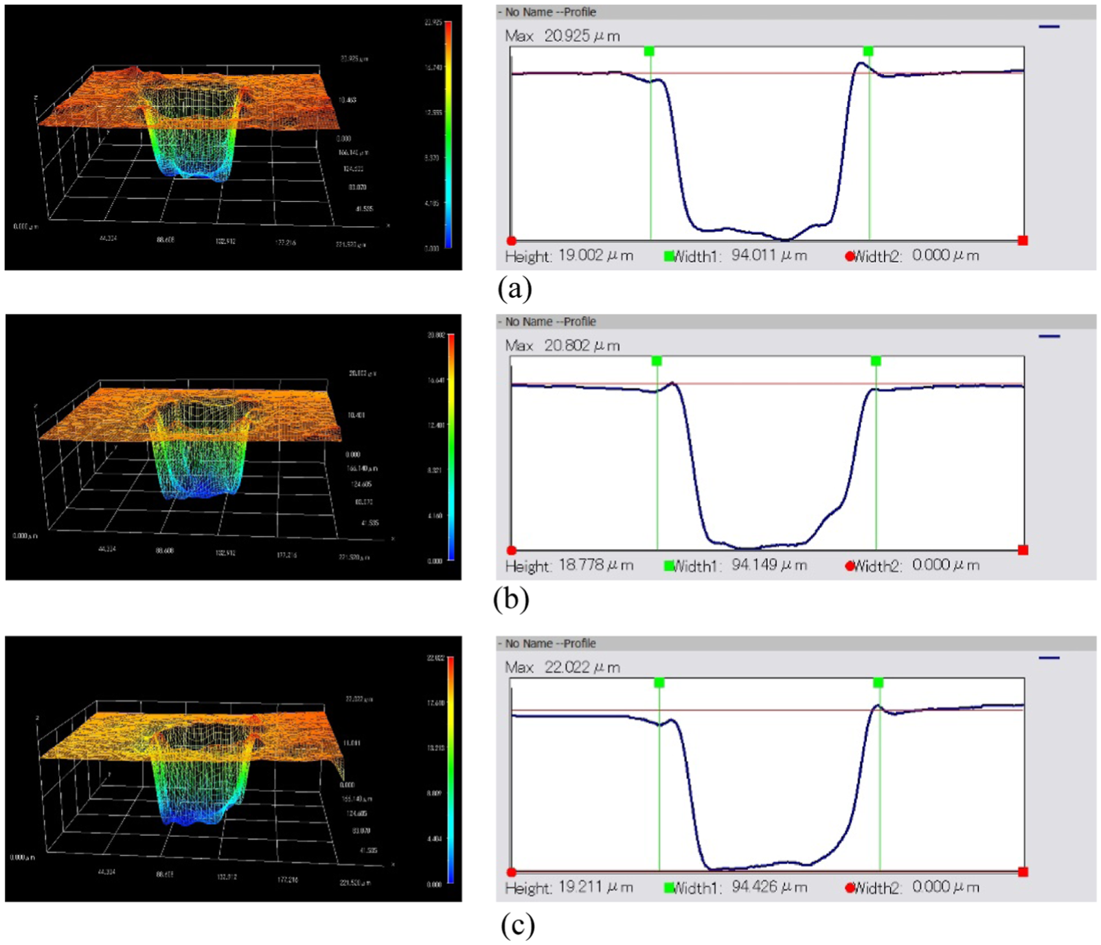
Three-dimensional profiles of micro-dimples at different locations: (a) edge, (b) half of radius and (c) centre.
Zhang et al. 28 fabricated square micro-dimple arrays with high machining accuracy using sandwich-like electrochemical micromachining with dry-film photoresist. However, the mask could only be used once and must be peeled off from the workpiece after machining, making it expensive for mass production. Compared to the dry-film photoresist, the PDMS mask is reusable and can short the lead time in fabricating micro-dimple arrays.
Conclusion
A new process for fabricating a PDMS micro through-holes mask has been proposed to generate large-area micro-dimple arrays. A combination of pressure and weight of electrolyte was demonstrated to successfully keep the PDMS closely attached to the workpiece surface during ECM, which is essential for achieving high machining accuracy. Based on the experimental investigations, the following conclusions can be drawn:
Large-area PDMS masks of length 100 mm and width 50 mm were fabricated successfully using a mould generated by WEDM.
The profiles of the micro-dimples were sensitive to pulse duty cycle. As pulse duty cycle increased, the depth of the micro-dimples decreased rapidly at the same effective machining time.
The present method improved machining accuracy of large-area micro-dimple arrays because the profiles of the micro-dimples were not sensitive to applied voltage, which weakens the effect of non-uniform distribution of electrical field on generating micro-dimple arrays.
Micro-dimple arrays of width 95 µm, depth 19 µm and a machining area of diameter 40 mm were successfully generated using PDMS mask, and the standard deviations of the micro-dimple width and depth were only 0.84 and 0.23 µm, respectively.
Footnotes
Appendix 1
Declaration of conflicting interests
The author(s) declared no potential conflicts of interest with respect to the research, authorship and/or publication of this article.
Funding
The author(s) disclosed receipt of the following financial support for the research, authorship, and/or publication of this article: This work was supported by the National Basic Research Program of China (973 Program, Grant 2015CB057502) and the Fundamental Research Funds for the Central Universities (NZ2016106).