
Abstract
Micromanufacturing processes are expanding in their length and breadth as long as the related research and development (R&D) activities and applications are concerned. Products are getting miniaturized and their performance efficiency is getting enhanced by the addition of micro/nanofeatures and devices. In the set of these two articles (Part I and Part II), an attempt has been made to review the latest R&D activities of the selected micromanufacturing processes. This article (Part I) deals with a review of the literature related to attrition (subtractive, or machining and finishing) processes (both types—traditional and advanced) including microturning, micromilling, microdrilling, abrasive jet micromachining, laser beam micromachining, electrochemical micromachining, magnetorheological finishing, abrasive flow finishing, magnetic abrasive finishing, ion beam micromachining and so on. Apart from the subtractive processes, an overview of the X-ray lithography has also been presented. An attempt has been made to report some applications to help the readers to evolve more new applications of these processes. At the end of different sections/subsections, some research areas have been identified, which would hopefully fill the gaps between the theoretical analysis, experimental work and applications.
Keywords
Introduction
Micromanufacturing has received great attention of researchers in the recent years because of various merits in the miniaturized products, namely, low material consumption, low energy consumption, lightweight and portable, high sensitivity (less energy requirement for actuation of a micro-component/product) and comparatively low cost-to-performance ratio. Micromanufacturing is the process of fabrication of micro part/product or creating microfeature on a large surface or component using different scaled down manufacturing processes. Nowadays, micro parts are becoming inevitable for a large number of products. This has provided significant impetus to develop new machine tools or modify the existing ones to use them for micromanufacturing. However, manufacturing of micro parts cannot be done by simply scaling down the size of the machine tool. There are many issues that are usually neglected during meso/macro-scale manufacturing, which are important during micromanufacturing. R&D activities in micromanufacturing related to machine tool design, process principle, theoretical analysis and so on are going on in different parts of the globe. Miniaturized products/systems have a huge demand for microelectromechanical systems (MEMS), micro-optical electronics systems (MOES), micro-reactors, fuel cells, micro-mechanical devices, micro-medical components and so on. Miniaturized products are widely used in automobiles, aircrafts, telecommunication, mobiles, computers, laptops, home appliances, medical devices and bio-implants. Many diverse strategies and methodologies are being developed to manufacture micro products/features.
Micromanufacturing processes include material removal (or subtractive), material addition (or layered manufacturing), joining and mass containing (microforming and microcasting) processes for fabrication of micro-components or for creation of microfeatures. Furthermore, nanofinishing is also an important area of micromanufacturing and it is widely used for fabrication of highly precise and close tolerance components. Figure 1 shows a general classification of micromanufacturing processes.
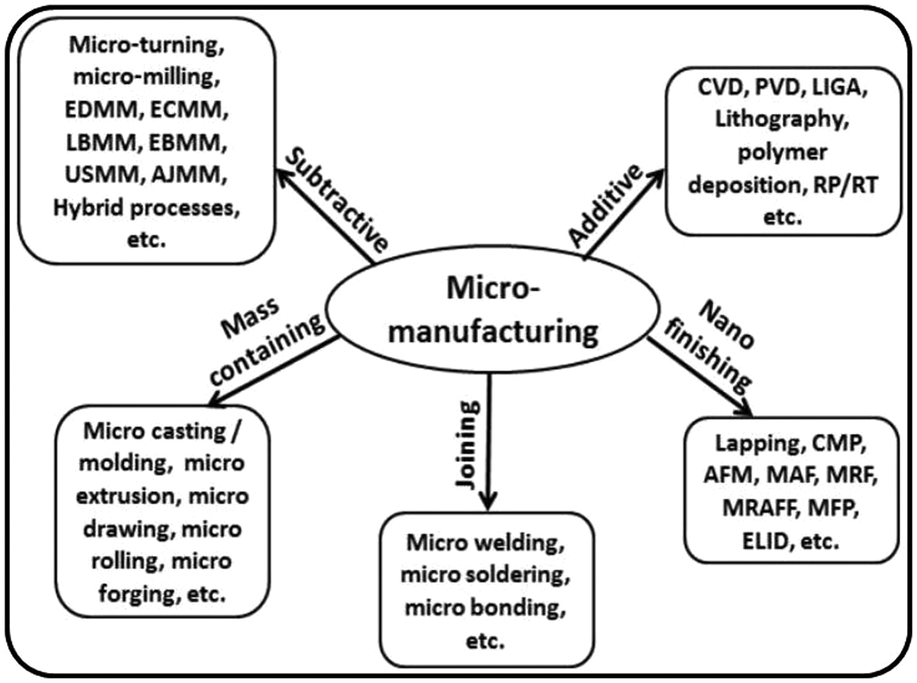
Classification of micromanufacturing processes.
In view of the space limitation, this review article has been divided into two parts: Part I deals with microsubtractive processes such as micromachining and nanofinishing, and lithography processes, while Part II discusses microforming, microcasting and microjoining processes. Since the material is being removed in case of both micromachining and nanofinishing processes; hence, they have been coupled together in Part I of the two review articles. Furthermore, in this review article, focus is on the mechanisms of material removal and related R&D. However, from operations’ sequence point of view, nanofinishing is always the last operation; hence, it could be kept in Part II in place of Part I. But operations’ sequencing is not our concern in these two articles. In these two articles, an attempt has been made to make a review of the available selected literature related to some of the micromanufacturing processes (Figure 1).
Microsubtractive (micromachining) processes
Micromachining is a process of creating submillimeter-sized component or feature on a micro- or macro-size component by removal of material in micrometer or even nanometer range. As shown in Figure 2(a), micromachining processes can be classified into three main categories: mechanical energy–based micromachining, thermal energy–based micromachining and chemical, electrochemical and biochemical energy–based micromachining. All these processes have certain merits and demerits; therefore, researchers have developed a few hybrid micromachining processes by combining two or more than two micromachining processes, to make it more efficient than the constituent processes and to expand the horizon of applications. Some of the hybrid processes are electrochemical spark micromachining (ECSMM), ultrasonic-assisted electric discharge micromachining (UA-EDMM), electro-discharge diamond grinding (EDDG), electrolytic in-process dressing (ELID) grinding and so on.1,2Figure 2(b) shows different types of abrasive-based nanofinishing processes classified into two categories: traditional and advanced nanofinishing processes.
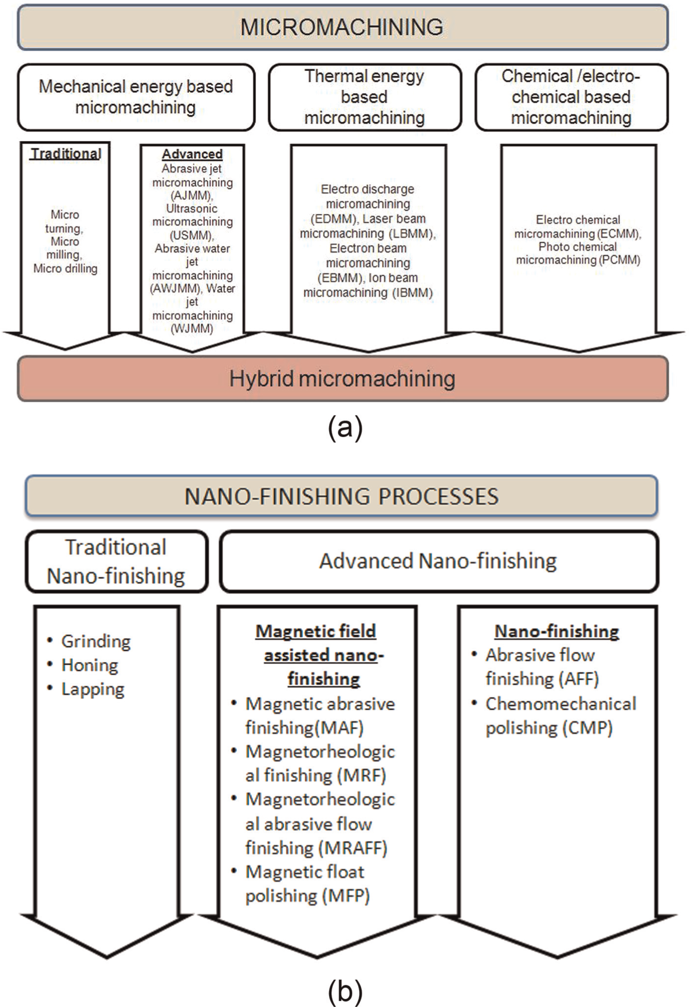
(a) Classifications of micromachining processes based on type of energy used and (b) classifications of nanofinishing processes.
Based on the period of evolution of micromachining processes, they can also be classified into traditional micromachining processes and advanced micromachining processes (AMMPs). 3 A review of micromachining processes of both these classes is given in the following sections.
Traditional micromachining processes
The commonly used traditional micromachining processes can be divided into three classes: microturning, micromilling and microdrilling.
In traditional micromachining processes, material removal takes place by physical contact between workpiece and tool. The tool has a well-defined cutting edge. These processes are widely used for making micro slots, micro holes and three-dimensional (3D) features. One of the most difficult tasks is fabrication of micro tools for these processes. Apart from grinding and polishing for making micro tools, electric discharge machining (EDM) and wire-EDM (or wire-electrical discharge grinding (WEDG)) are also used as alternative methods to fabricate micro tools for these processes. 4 The stiffness and strength of a micro tool depend on its size (diameter or cross section) and length. Tool for microdrilling is subjected to torsional moment. It is also subjected to thrust force, which causes buckling and transverse force that causes bending. In case of micromilling tool, torsion and side bending occur during machining. 5
Micro tools are made of mono crystalline diamond, tungsten carbide or cubic boron nitride (CBN). If a micro tool is made of mono crystalline diamond, then its use is limited to nonferrous and non-carbide forming materials due to diffusion of carbon from the diamond tool. In case of hard metals, it is very difficult to get a sharp and uniform cutting edge. Generally, micromachining by micromilling or microdrilling is carried out at comparatively low rotational speed (r/min) of the tool, resulting in low material removal rate (MRR). However, it is necessary to consider some factors before selecting revolutions per minute of a tool such as tool life, true running accuracy, stability of tool and dynamic behavior of machine.6,7 A brief review of the mechanical micromachining processes is presented in the following sections.
Microturning
Microturning is an ultra-precision machining process to generate features of small dimensions with sub-grain level of uncut chip thickness. Microturning significantly differs from macro/mesoturning in many ways, notable among them are the following: the diameter of the component being machined is generally smaller than 1 mm; sub-grain cutting mechanism that is the chip cross section is generally smaller than the grain size of workpiece material and lack of rigidity of the workpiece results in deflection of the component. The tolerance on the component in microturning is difficult to maintain in the same ratio as in macroturning; the size of the machine is smaller and it should be highly accurate to achieve such uncut chip cross sections. In view of these, micromachining cannot be achieved by simply scaling down the macro/mesoturning process parameters and the machines. Even though the microturning is practised over a century by watch-making industries for very specific products, the research in this area is not widely pursued and published due to the lack of applications till late 1980s.
Undesirable effects on the microturned components, namely, variation in shape, size and surface finish, are caused by different factors like machine tool accuracy, cutting tool geometry, work material properties especially hardness and grain size, cutting parameters, machining sequence and thrust force generated during cutting. Since the material removal takes place at sub-grain level, feed and depth of cut need to be controlled precisely; hence, microturning machines are built with very high level of positioning accuracy and repeatability. Rigidity of the machine tool affects size, shape and surface finish control; lack of rigidity also causes tool and component to vibrate during microturning process. Requirement of high response of the moving parts necessitates the total machining system to be small with low inertia. Therefore, machines for microturning need to be built with very high level of accuracy, rigidity and fast response.8–10
The shape and size of a microturned component are mainly affected by thrust force. Cutting tool geometry, particularly tool cutting edge sharpness and tool nose radius, significantly affects the thrust force acting during machining. The thrust force in conjunction with frictional force causes center height of the component with respect to the tool to change; this change subsequently causes the component to ride over the tool rake face and bend or break. Balancing reaction force to the thrust force is the effective way of overcoming this problem. Machining with multiple tools mounted in the same plane and application of “step-type turning” instead of turning the entire length continuously are some of the common methods employed to balance the thrust force.11,12 A typical micro shaft is shown in Figure 3.
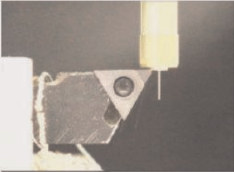
Microturning with PCD tool (micro-shaft diameter 0.05 mm × 2 mm long).
There exists a correlation between the cutting edge sharpness and uncut chip thickness for efficient cutting. When the uncut chip thickness is smaller than a certain threshold value, for the given cutting edge sharpness, either rubbing or burnishing takes place and when it is more than the threshold value, material is removed by shearing in ductile material and by brittle fracture in brittle material. Since smaller uncut chip thickness is aimed in microturning for better control of size, shape and surface finish, the cutting edge radius becomes very critical. Larger tool nose radius causes higher thrust force and conditions for chatter, whereas smaller tool nose radius results in increased tool wear. However, larger tool nose radius results in better surface finish on the component. 13 Hence, optimum values of tool nose radius and sharpness of cutting edge are the critical requirements of microturning. 14 Furthermore, grain size of the workpiece significantly affects cutting force during machining, as the grain size of the workpiece increases, the thrust force as well as the deflection of the workpiece increases. 15
Diamond turn machining
Diamond turn machining (DTM), which is also called as deterministic nano regime machining process, is capable of controlling the size tolerance, shape error and surface finish within few tens to few hundreds of nanometer (nm) on nonferrous materials using ultra-sharp single-crystal diamond tools. Since DTM is a path-controlled process, the machine tool accuracy needs to be extremely high; a typical DTM machine has a spindle run out of 20 nm and positioning accuracy of the tables within 10 nm. Machines for DTM incorporate various features like vibration isolation for the entire machine, hydrostatic tables to have better damping, water-cooled aero static spindle head and online tool off-set measurement system, to achieve nanofinishing on optical quality surfaces. To achieve optical quality on machined surfaces, applying very small uncut chip thickness, combination of ultra-precision machine along with high-quality single-crystal diamond tool with predefined crystallography orientation and sharpness to the tune of less than 200 nm is employed. Large number of research publications is made from the middle of the last century in the areas of machines for DTM and single-crystal diamond tools.16–19 Experimental studies including machining of various optical materials like silicon and germanium, optimization of machining parameters and tool wear studies were some of the major research areas that were explored by many researchers.20,21 Research work in the area of material removal mechanism by nano cutting/DTM led to the emergence of newer areas like application of molecular dynamic simulation (MDS) and ductile regime machining of brittle materials.22,23 Since metal and nonmetal optic applications are continuously increasing, DTM is becoming popular not only in academic research but also in industrial domain. Many advances are still taking place in the area of DTM. Application of DTM in aspheric surfaces integrates facilities like online or offline measurement of the generated surface with DTM to regenerate corrected tool path automatically for subsequent machining; other developments include application of fast tool servo and freeform machining to generate complicated 3D surfaces.
Micromilling
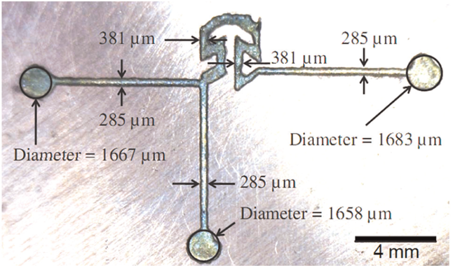
Micromilling is an important process in the manufacture of micro- and meso-scale products, and it has an advantage of creating complex 3D geometry in a wider variety of materials. 24 Figure 4 shows a typical stainless steel Y-mixer manufactured by micromilling, which efficiently mixes two different fluids by diffusion process. The mixer has two input ports through which the fluids to be mixed are admitted under pressure. When the fluids pass through the serpentine microchannels, they get thoroughly mixed and the mixture reaches the collection reservoir. Even though the micromilling process mechanism is similar to that of macromilling, it cannot be considered as a scaled down version as it involves a number of other issues.
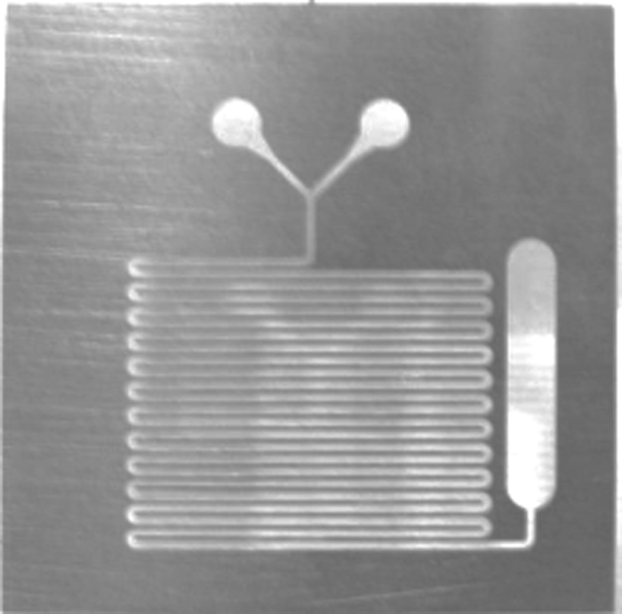
Micromilled Y-mixer (microchannel depth 100 μm × width 270 μm).
Micromilling phenomenon differs from macromilling due to size effects; the cutting edge radius of a micro tool is comparable to the uncut chip thickness, resulting in cutting at large negative rake angle. 25 This is particularly evident at low feed rates, where the effects of ploughing are more significant. 26 In micromilling, specific shear energy increases significantly when the uncut chip thickness is smaller than the minimum chip thickness due to ploughing phenomenon. 27 Elastic recovery increases friction between the flank face of the tool and the workpiece and amplifies the effect of process damping. The size effect due to material specific cutting force at the micro-scale is much higher than at the macro-scale and it makes micromilling of difficult-to-machine materials even more hard. 28 High specific cutting force cannot be sustained by a micro-sized tool, which usually results in a catastrophic failure of the tool and poor surface finish.
One of the challenges in micromilling is regenerative chatter due to changes in chip thickness that causes severe wear and breakage of the tool.29,30 Since the tolerances are generally tighter, the chatter can cause serious damage to the generated micro-scale feature. Most of the tools employed in micromilling process are fragile in nature, and it is a major source of tool failure. Small chip thickness is used to minimize excessive loads, to prevent tool breakage and to avoid large tool deflection. Interrupted cuts cause variation in cutting force and lead to tool failure. The study on the effects of vibration parameters on the surface roughness and tool wear 31 indicates that two-dimensional (2D) vibration-assisted micro-endmilling can reduce surface roughness and tool wear as compared to traditional micro-endmilling. Unlike macro machining processes, the size and volume of the burrs generated in micromilling are comparable to the size of the generated microfeature itself. 32 A proper machining strategy to minimize generation of burrs in micromilling is important because their removal and subsequent edge conditioning result in degradation of the micro-milled feature. At times, loosely attached chips and burrs interfere with the tool and lead to breakage. Prediction of burr height in micro-endmilling is challenging due to complex geometry of material removal and microstructural effects encountered during cutting at that length scale. 33
Microdrilling
Microdrilling still stands as the most popular machining operation for product manufacturing. There are several methods for making micro holes using AMMPs as discussed in the following sections. Each of them has its own merits and limitations concerning the machining capability, investment cost, running cost, workpiece material properties and so on. However, mechanical microdrilling is widely used because it can produce holes with good roundness, straightness and surface roughness in a short processing time.34,35 Mechanical microdrilling has been used to drill 50-μm-diameter hole in a human hair at Bhabha Atomic Research Centre (BARC), Mumbai, India. Unfortunately, mechanical microdrilling is not an easy machining process due to poor stiffness of the tool, difficult-to-remove burrs, difficulty in accurate-positioning of the tool and so on. It is difficult to supply cutting fluid to the cutting zone and to remove chips in case of deep hole drilling including high aspect ratio (HAR) hole; most of the time, the machining state becomes unstable and the tool breaks.36,37 Other difficulties in HAR microdrilling are wandering motion during inlet stage and high temperature at the drill tip. The most undesirable difficulty is an increase in drilling force and torque as the drill penetrates deeper into the workpiece due to chip-related effects. Peck-drilling is thus widely used for deep hole drilling despite the fact that it leads to low productivity. Although conventional machining and micromachining show many similarities, the cutting parameters of conventional machining, like cutting speed, feed and depth of cut, cannot be off hand down scaled into micro range due to the size effects. 38 The size effect has a major impact on the cutting forces, process stability and resulting surface finish in microdrilling.
One of the significant reasons for tool breakage in microdrilling is burr–drill interaction especially at the exit side of the hole. When the helical flute of the rotating tool encounters the exit burr—whose thickness is gradually reducing from the root to the top of the burr—the free end of the burr, which is very thin, entangles with the drill and exerts undue torque on it and leads to the tool breakage. Hence, prevention of exit burr formation will enable to reduce tool breakage in microdrilling. During drilling with conventional size drills, decreasing drill diameter decreases the burr size, while in microdrilling, 39 below a certain critical drill size, the burr size begins to increase.
AMMPs
These processes can be classified into three basic groups: mechanical energy–based advanced micromachining, thermal energy–based micromachining and chemical and electrochemical energy–based micromachining. A brief review of the selected AMMPs from each group is presented in the following sections.
Mechanical energy–based advanced micromachining
Abrasive jet micromachining (AJMM), water jet micromachining (WJMM) and abrasive water jet micromachining (AWJMM) are more or less similar in terms of configuration of machines as well as principle of material removal. The only difference is in the supply of machining energy in the form of abrasive particles jet, water jet or mixture of abrasive particles and water jet. Figure 5 shows a schematic diagram of these processes. These processes are widely used for micromachining of glass, polymethylmethacrylate (PMMA), elastomers and polymers such as polydimethylsiloxane (PDMS), acrylonitrile butadiene styrene (ABS), polytetrafluoroethylene (PTFE), metal sheets and ceramics.40–42
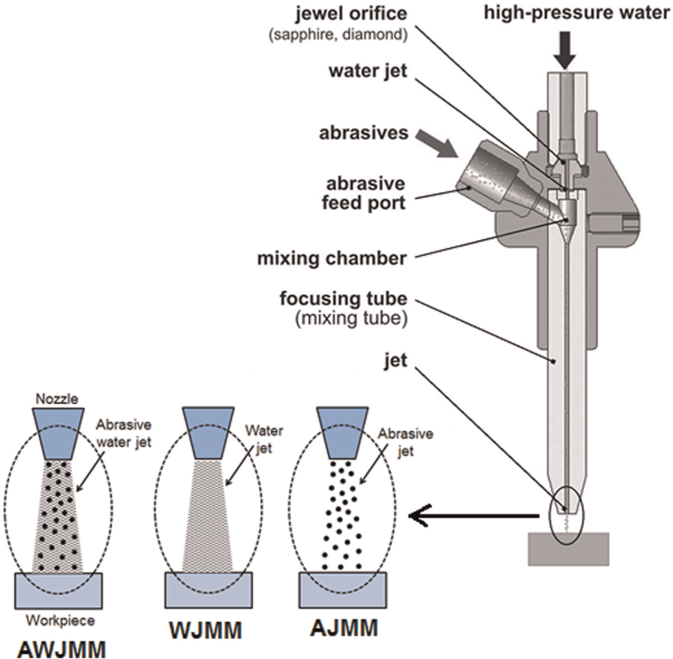
Schematic diagram of AWJMM, WJMM and AJMM processes.
One of the major issues in using these processes in micromachining domain is the control of stream of abrasive particles and water to the smallest possible diameter. Since the feature size is in micrometer range, the diameter of the stream should be smaller than the feature size, to account for overcut. There are many parameters that affect the size of contact area in these processes such as standoff distance, diameter of nozzle and pressure. Therefore, many times, masking of workpiece surface is required to minimize or eliminate the damage to the machined surface. 43
Extensive work has been done related to macro-scale machining by these processes. The efforts are being made to make these processes applicable to micro domain and complex 3D machining. Some of the gray areas of research for these processes are as follows:
Modeling is one of the areas that need more work to be done, related to understanding the jet characteristics and its performance. Modeling of these processes generally concentrates on the calculation of volumetric MRR, interaction of abrasive particles (in case of AJMM and AWJMM) or water jet (in case of WJMM) with workpiece.
3D microcutting ability is one of the thrust areas of any micromachining process. It is necessary to develop multi-degree freedom of movement of jet for cutting complex shapes. Computer numerical control (CNC) feature added to these machines would play an important role in achieving these movements.
Research work also needs to be focused on extending the applications of these processes to the operations such as turning (say, abrasive water jet microturning), nanofinishing, microdeburring and similar others.
Use of nano-size abrasive particles is necessary to reduce the size of overcut and to improve accuracy of the feature to be machined. However, mixing, storage and flow of very fine abrasive particles are not as easy as that of bigger size abrasive particles. Therefore, new methodologies and techniques are necessary for dealing with such issues.
Ultrasonic micromachining (USMM) is widely used for machining ceramics and other brittle materials irrespective of electrical conductivity of workpiece material. It consists of a tool vibrating system and abrasive slurry feeding system. The tool is vibrated at high frequency (≈20–40 kHz) with amplitude of vibration in micrometer range. The slurry consists of micron-size abrasive particles and liquid medium. It is fed into the gap between the vibrating tool and the workpiece. When the vibrating tool hits the abrasive particles, they attain momentum and impact workpiece surface resulting in micro chipping. Extensive research work has been done on macro USMM. However, USMM has not been explored to that extent. 44 Use of USMM for micromachining is challenging because of micro tool, micro/nano-size abrasive particles and its feeding system.
The stability of tool against vibration and bending during machining significantly affects dimensional accuracy of the feature to be created. A new method was proposed 45 in which vibrations were given to the workpiece instead of to the tool. This has enabled a better tool holding and use of a high-precision spindle mechanism. Using WEDG technique, tools of various types ranging from 5 μm to several hundred micrometers are easily produced with good reproducibility. Straightness and repeatability are the main issues for fabrication of micro tools by WEDG, which can be taken care of, by selecting appropriate levels of process parameters. 46
Tools for USMM are generally made of stainless steel, brass or mild steel to reduce tool wear. Some researchers have also proposed a viscoelastic thermoplastic composite material for fabrication of tools for USMM process. 47 In situ tool manufacturing is a good solution to the problem associated with micro tool mounting. A small deviation in mounting of micro tool results in noncircular hole and tool breakage. Microfeature machining by USMM faces another challenge of handling of very fine abrasive particles such as uniform distribution in the slurry, effective removal of abrasive particles from the machining zone and cleaning of machined components.
Thermal energy–based micromachining
Thermal energy–based micromachining processes use high-intensity heat as a machining tool, which is produced by different ways such as laser beam, electron beam, sparking or plasma column. HAR structures can also be fabricated by appropriate selection of process parameters. However, some disadvantages of these processes are heat-affected zone (HAZ), recast layer, vacuum environment (in case of electron beam micromachining (EBMM)), thermal residual stresses and so on. Therefore, selection of the process depends on the quality, cost and time required for micromachining the component.
EDMM is a widely used process for fabrication of microfeatures on difficult-to-machine but electrically conducting materials. EDMM is a process that can be used for performing operations such as milling, drilling, turning and grinding. Recently, it has been employed for nanofinishing of hard materials. 48 The philosophy behind employing the EDMM process for nanofinishing is to create the craters in nano size. When these craters overlap with each other, much better surface finish is obtained. Nano-size craters can be achieved by substantially lowering down the values of input parameters. A variant of EDMM is wire-EDMM used for fabrication of micro tools for other micromachining processes, 49 dies for metal forming processes and others. Jahan et al. 50 developed HAR micro tool electrode on the EDM machine, and then the same tool was used on the same machine without disturbing setting, for vibration-assisted ED microdrilling in tungsten carbide. Applications of ceramic materials increase substantially due to some of the favorable properties such as high hardness, heat resistance and oxidation resistance. The presence of electrically conductive secondary phase makes it possible to machine them by EDM. Several applications of micro EDM are demonstrated by machining of ceramic composites such as Si3N4-TiN 51 and ZrO2-TiN 52 for fabrication of micro-compressor, 3D gas turbine impeller, micro molds, micro extrusion die and air bearing components.
Sophisticated drives and instrumentations are required for making EDMM more efficient in machining microfeatures. Some of the advancements in equipment technology of EDMM are as follows:
EDMM machines use ball screws in servo drives for different axes. Precise and quick movement of z-axis is very important. Linear motors are more powerful and precise than ball screws to avoid backlash. Fast movement of electrode improves machining speed and flushing, which results in better surface finish.
High level of automation of EDMM process improves output and accuracy of the product. Robotic transfer of tool electrode from its fabrication point (CNC milling or any other process) to the EDMM machine spindle and then its automatic loading/unloading would reduce man-made errors. In such a way, round the clock utilization of EDMM machine would become feasible.
Electrode wear in EDMM makes it difficult to accurately calculate machining time and to achieve the desired shape and size of the feature/product. Therefore, the philosophy of in-built electrode wear compensation of CNC EDM can be employed in case of EDMM process also.
Very fine tuning of spark energy is required for machining of micro-components as well as microfeatures. Advanced spark generator circuit enables finer control of the spark and its waveform. A closed-loop CNC system is required for monitoring of spark and to take corrective action if need arises.
In ED micromilling, selection of a suitable type of dielectric fluid is important. Chung et al. 53 have used deionized water in place of kerosene as a dielectric fluid. Machining characteristics during ED micromilling, such as tool wear, interelectrode gap (IEG) and MRR, were investigated. Micro hemispheres were milled to study machining efficiency of kerosene and deionized water as dielectric fluid and they were compared.
It is reported that during micro-ED milling, the problem of electrolytic corrosion arises because workpiece material used was susceptible to electrolyzation. To solve this problem, a mixture of compressed air and deionized water spray was injected into the machining gap, and high-quality micro grooves were machined on the WC-Co workpiece with no electrolytic corrosion and minimum possible electrode wear. 54
EBMM, laser beam micromachining (LBMM) and ion beam micromachining (IBMM) are the beam-based processes. Intense heating of workpiece by beam (except ion beam) results in material removal at micro/nano level. Therefore, they are widely used for fabrication of complicated features, drilling holes, fabrication of nanostructures and many more. EBMM has been used to fabricate filters for textile and food industries having holes as small as 6 μm diameter, 200,000 holes/cm2 as holes density and taking about 2 μs/hole as drilling time. Research has also been focused to reduce HAZ using pulsed electron beam. Laser-assisted micromachining (LAMM) is a promising technology offering desired capability of producing complex 3D and HAR microfeatures in various difficult-to-machine materials.
Apart from the above applications, LAMM has been used for micro/nano texturing or structuring. Furthermore, LAMM is a maskless process for fabrication of micro/nano-scale devices that are used in electronics, MEMS and medical components. Photolithography is a widely used process for fabrication of the above components that require a master mask to transfer patterns onto a substrate. Therefore, laser direct imaging (LDI) is an alternative process to reduce processing or fabrication time for making micro-scale structures on printed circuit boards, glass and epoxy. 55 Micro patterning on biodegradable polymers is also attempted by ultraviolet (UV) and femto-second laser for development of drug delivery and tissue engineering devices. 56 Application of femto-second laser pulses is found in fabrication of silicon photovoltaic cells. 57 In this application, laser pulses are used for reducing solar light reflection by fabrication of micro-spikes on the silicon surface. One of the problems of LAMM is thermal damages, which occur during melting and vaporization of workpiece material. These damages to workpiece surface and subsurface occur due to excessive heat and redeposition of ejected molten materials. Effect of such damages is significant when the feature size is micron or submicron. The damages can be minimized to certain extent by pico- or femto-second pulse lasers. However, the cost and capability of ultra-short-pulsed lasers make them unsuitable for high MRR applications. Therefore, other inexpensive yet efficient technique such as water jet–assisted laser micromachining can be used to reduce thermal damage to the workpiece. 58
Modeling of thermal energy–based micromachining processes has been attempted by various researchers.59,60 However, the main problems in modeling are the application of appropriate type of heat source and prediction of heat dissipation in the material, atmosphere and so on. As a result, extensive experimental data are required to understand the workpiece–energy interface in different types of materials.
Electrochemical and chemical energy–based micromachining
Chemical energy–based micromachining processes use acidic chemicals to remove material, while electrolyte is used in case of electrochemical micromachining (ECMM) for anodic dissolution of workpiece material. ECMM is an anodic dissolution process where an electrolytic cell is formed by connecting tool to the negative terminal (cathode) and workpiece to the positive terminal (anode). When a suitable electrolyte (acid, basic or neutral) flows through the IEG between workpiece and tool with appropriate applied voltage (2–5 V), material is removed from the anode (workpiece) according to Faraday’s laws of electrolysis. 61 This process has some advantages over other processes such as good surface finish, absence of residual stresses, theoretically no tool wear, no burr formation and no distortion of the features. Furthermore, the use of ECMM with a CNC machine has been extended to milling, 62 multiple hole drilling 63 and surface structuring. 64 Figure 6 shows a micromixer fabricated using ECMM process and the width of the microchannel ranging between 180 and 300 μm. 65
Micromixer fabricated using electrochemical micromachining process.
In ECMM, control over the region on which material removal is taking place is important. Therefore, insulation of tool surface and masking of workpiece surface are required to get high-dimensional accuracy. Undercut can be minimized by this technique. 2 Figure 7 shows a diagram representing a tool with mask and exposed area (top view) under which machining is to take place on the workpiece. IEG is the machining gap in which electrolyte flows. It also shows undesirable undercut obtained during the ECMM process (front view).
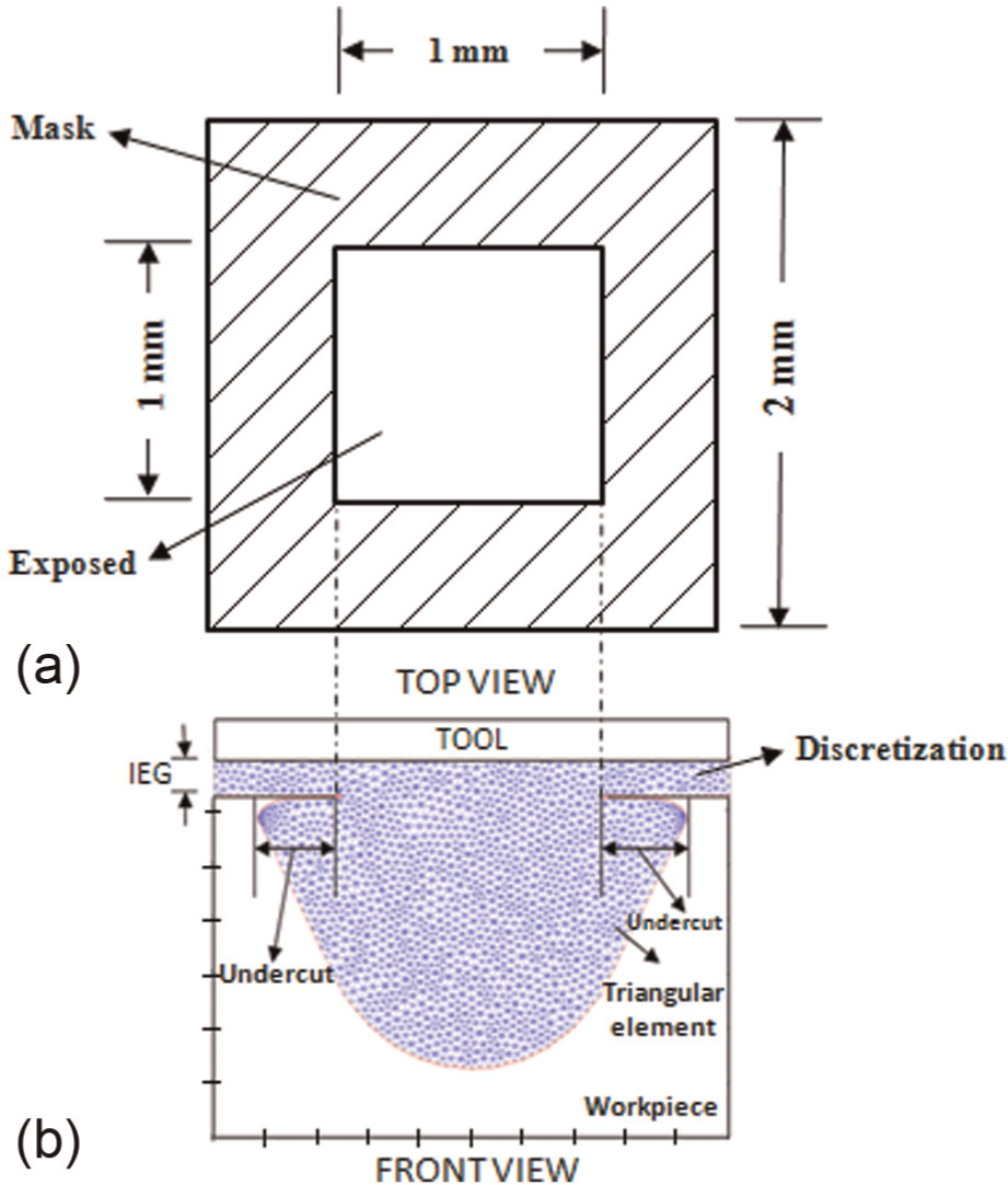
(a) Schematic diagram of the mask. (b) Machined workpiece domain and interelectrode gap with discretization.
In photochemical micromachining or wet chemical etching, material is removed by oxidation in the presence of chemical etchant, which reacts with workpiece surface. For a better control of dimensions, masking is applied over workpiece surface to avoid or minimize unwanted material removal as well as undercut. 61 In this process, electrical conductivity of the workpiece is not a prerequisite and machining or etching takes place purely by chemical reaction. Therefore, selection of appropriate etchant, material for masking and machining time are the important parameters to fabricate the desired microfeatures. To minimize the undercut, design of the tool, design of the mask and optimization of machining parameters are essential.
Focused ion beam machining
In case of ion beam micro/nano-machining, the material is removed atom by atom by the mechanical impact of ions on the top surface of the target. In this case, melting and vaporization of workpiece material do not take place. It is an extremely slow process as compared to other processes and very much suitable for nano fabrication by both subtractive and additive processes. 66
Focused ion beam (FIB) technology has high potential applications in the fabrication of small structures to make products with feature sizes at micro/nano-scale. It also facilitates fabrication of 3D structures. Not only machining, FIB is also used as a tool for additive micromanufacturing through the deposition process. This technology is also used for fabrication of micro tools/micro dies of cemented carbide and diamond for imprinting features on the workpieces made of material other than silicon.
In IBM, ions hit the atoms on the surface of the workpiece. If ion energy hitting the atom is greater than the bonding energy of the atom, then the atoms are separated out one by one from the workpiece. If ion energy is much higher than the bonding energy of an atom, then it will sputter off many atoms at a time and the ion itself may get implanted inside the workpiece leading to a defect. The depth etch rate (dz/dt) for a sputtering yield of Y surface atoms per incoming ion, using a probe of current I, is expressed as follows 67
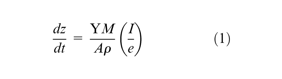
where A is the etched area, ρ is the target material density, M is the atomic mass of target material and e is the electron charge.
Gases are used for enhancing both material removal (machining) and deposition of metals on the target material. Precursor gas containing the elements to be deposited is passed through a capillary gas feeding nozzle on the substrate. Precursor gas molecules condense and an adsorbed layer is formed.
Microstructured diamond tools have been fabricated 68 using FIB machining. Such tools can be used for mass patterning/printing/stamping on the metallic and nonmetallic workpieces. There are many other applications reported in the literature, which deal with the fabrication of microcutting tools, multipoint cutting tools, tissue stabilizer and many other biotechnology-related applications.69,70
Additive/layered micromanufacturing
Apart from the material removal-based micromanufacturing (also known as top to bottom approach), additive micromanufacturing is also emerging as a promising technique (also known as bottom to top approach). Different types of additive micromanufacturing processes such as micro-stereolithography, ink-jet printing, selective laser sintering and 3D printing are used to fabricate micro-components for medical and biomedical devices, automotives, dies and molds, jewelries, electronics, aerospace and so on. 71 3D printing is being called as the third industrial revolution following mechanization in the 19th century and assembly line mass production in 20th century. Recent trends also show the application of additive manufacturing in custom-made 3D porous ceramic scaffolds for bone replacement with fully interconnected channel network for the repair of osseous defects from trauma or disease. 72 Ceramic microstructures such as gears, tubes and array of pillars are also fabricated by micro-stereolithography 73 and ink-jet printing. 74
An important benefit of additive micromanufacturing is its ability to make complex internal feature in only one step. Layered manufacturing may provide solution to the wide range of products related to medical, tooling, aerospace, architecture, consumer goods and so on. 3D printing or layered manufacturing changes the calculus of manufacturing by optimizing for batches of one, flexibility to build a wide range of products and making products without tool. It is leading toward a factory without machine tool, production lines, tooling and assembly lines and leading to minimum possible lead time.
3D printing is a factory without a factory floor and it has created a platform for innovation, enabling manufacturing to flourish in uncommon areas. Using 3D printing, researchers at the Vienna University of Technology have produced a race car approximately 285 μm long in 4 min. It is being applied for making kidney, hearing aid and so on. Intensive research activities are going on at GE Aviation to produce plane engine 1000 pounds lighter. 75
Nanofinishing processes
Finishing processes can be broadly classified into “traditional finishing processes” and “advanced finishing processes” (AFPs) The later can be further classified into magnetic field–assisted nanofinishing processes: magnetic abrasive finishing (MAF), magnetorheological finishing (MRF) and so on and general nanofinishing processes: abrasive flow machining (AFM), chemo-mechanical polishing (CMP). Final finishing of the components is necessary to make them suitable for performing their functions satisfactorily as well as to increase their service life. Nowadays, many finishing processes are in use to finish different types of components, which require surface finish in the nanometer range. It is very difficult to achieve this level of surface finish by means of conventional finishing processes, namely, grinding, lapping and honing. As a result, a new class of finishing processes called AFPs has evolved. A brief review of these AFPs is presented in the following sections.
CMP
CMP was developed at IBM for defect free and highly reflective silicon wafer surface finishing for semiconductor industries.76,77 CMP is basically a surface planarization technique where emphasis is to achieve sub-nanometer surface roughness value along with planarization. It is also used for finishing of dielectric materials such as ceramics, mica, glass and plastic. CMP uses slurry that consists of submicron-sized abrasive particles and chemicals. In this process, a silicon wafer is held at the bottom side of the rotating wafer carrier and a polishing pad is fixed over rotating table. Polishing pad has micro fibers that retain abrasive particles supplied by slurry feeding system. Relative motion between wafer and abrasive particle–laden polishing pad results in material removal from silicon wafer at micro/nano-scale. Since the CMP includes both mechanical abrasion and chemical interaction between slurry and workpiece surface, modeling for MRR is rather complex. Researchers have developed models of MRR by incorporating different theories such as contact mechanics, elasticity and bending as discussed in the following.
The well-known equation for modeling of CMP is the Preston equation. 78 It is the basic equation for calculation of MRR by considering pressure applied on the workpiece (P) and relative velocity (U) between abrasive particles and workpiece surface

where k is a Preston coefficient that depends on surface chemistry, workpiece–pad interaction, abrasion effect and so on. Researchers have modified the basic equation of Preston by introducing different terms of CMP process in place of coefficient “k.”
Shi and Zhao 79 considered soft pad and workpiece interaction to modify Preston’s equation. Abrasive particles interact with pad and wafer, and it was found 80 that large deformation between the pad and abrasive particles plays a significant role in force balancing. Preston’s equation is modified by considering polishing efficiency and dynamic friction coefficient. 81 An integrated model has been proposed 82 for evaluating wafer surface evolution during the CMP process. A new MRR model has been developed 83 using micro-contact mechanics and particle size distribution theory, including chemical role of the slurry, wafer properties, pad surface profile and so on. Recently, an integrated model has been proposed 84 that incorporates the effects of properties of particles, wafer and polishing pad, and process parameters as well as contact zones (wafer-particles, pad-particles). However, a more comprehensive theoretical model incorporating CMP process parameters is required to predict MRR compatible to the experimental results.
MRR is found to increase with decrease in abrasive particle size,85,86 while others87,88 observed the contradictory results. Apart from this, some researchers 89 observed that MRR increases initially up to a certain level with increase in abrasive particle size, beyond which it starts decreasing. Under such situations, one needs to carefully analyze the process and the results before reaching any generalized conclusion.
There are many unexplored areas of CMP including modeling. Many MRR models have been developed by researchers, but an integrated comprehensive model of CMP is still to be developed. It is also desirable to combine two or more developed models in such a way that the new model is able to correctly predict the responses comparable with experimental results. For this, both mechanical abrasion and chemical interaction between abrasive particles and workpiece surface should be accounted. Jain et al. 90 combined CMP and MRF processes to develop a hybrid process (chemo-mechanical MR finishing), which is capable to give surface roughness value on a single-crystal silicon blank as good as 0.48 nm. Modeling of such processes is still more difficult because it involves mechanical abrasive, chemical dissolution, magnetic force and magnetic field that affects the rheological properties of the finishing medium.
Abrasive flow finishing
Abrasive flow finishing (AFF) is a widely used process for finishing, deburring, and radiusing of inaccessible areas, holes, internal cavities, external surfaces, molds and dies, gears and so on. 91 AFF uses abrasive particle–laden polymer-based viscoelastic mixture called medium (also named as self-deformable stone) 3 for finishing. The medium is extruded back and forth to finish the workpiece between two vertically opposed cylinders (Figure 8). The abrasive particle in the medium works as a cutting tool for abrading workpiece surface. One of the most important parts of AFF process is the tooling, which guides flow of the medium over or through workpiece surface. 92 Rheological properties of abrasive medium, extrusion pressure, initial surface finish, finishing time and so on also play important role in governing surface roughness value of the finished surface and finishing rate (FR). 93
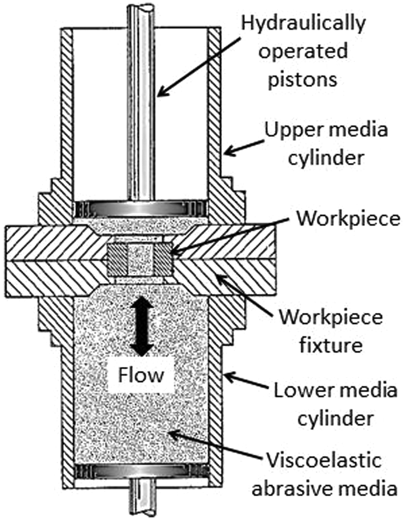
Schematic diagram of AFF process.
Experimental work related to AFF process has been extensively reported in the literature, but very few researchers have worked in the modeling of AFF process. A mathematical model to study the characteristics of the abrasive-laden medium using Maxwell and Kelvin Voigt model was proposed. 94 Jain and Jain 95 proposed a finite element (FE) model for analyzing flow of a viscoelastic medium in the AFF process. The material removal and surface roughness are studied based on the finite element method (FEM) results. The medium is considered as a polymer-based non-Newtonian viscoelastic fluid. FEM was used for evaluating the resultant pressure, velocity and radial stresses in centrifugal force–assisted AFF. 96 FE model is developed to predict forces acting on an abrasive particle for calculation of material removal from a complex external cylindrical surface. The medium is assumed to be viscoplastic instead of viscoelastic, which is a drawback of this model. It is reported 97 that long piston stroke results in high FR due to an increase in wall shear stress. However, wall shear stress depends on the extrusion pressure and medium viscosity. To study thermal aspects of AFF process, a model of specific heat capacity of the medium was developed 98 considering the mass proportion of each constituent. The developed model considered heat flow in the workpiece and medium in AFF process using one-dimensional unsteady-state heat transfer theory. However, higher dimensional (2D and 3D) model with the same approach needs to be developed for a better understanding of the process. Lately, a model was proposed 99 to evaluate forces acting on the workpiece considering the fundamental theory of grinding and compared theoretical results with the experimental observations.
An important and difficult part of modeling of AFF process is viscoelastic medium properties and the presence of abrasive particles in it. Furthermore, effect of temperature during the process needs to be investigated and modeled because viscosity of the medium is significantly affected by the temperature. As a result, models with constant temperature do not represent actual behavior of the AFF process. A relationship between temperature and medium viscosity would provide more insight into the medium characteristics and its effects on the AFF process performance.
Magnetic field–assisted finishing processes
MR fluid-based finishing (MRFF) processes
CMP and AFF processes do not have determinism in terms of externally controlling forces acting on workpiece surface. There is another group of processes in which the forces acting on workpiece surface can be controlled in real time by changing the magnetic field. Some of such processes are MAF, MRF, magnetorheological abrasive flow finishing (MRAFF), magnetic float polishing (MFP) and so on. 1 The researchers have developed different types of apparatus for finishing various size and shape of components. However, working principle or mechanism of material removal in these processes remains almost similar.
MAF uses either sintered ferromagnetic abrasive particles or homogeneous mixture of abrasive particles and magnetic particles with a little amount of oil as a binder, while MRF and MRAFF processes use MR fluid that consists of magnetic particles (normally greater than 1 μm size), abrasive particles, water or oil as a carrier fluid and some additives. MFP uses magnetic particles (magnetite) of very fine size (10–15 nm) and abrasive particles in a carrier fluid with some surfactant. 2 Singh et al. 100 conducted MAF experiments to measure forces acting on the workpiece and to find out critical surface roughness value using non-magnetic workpiece material. First time, they used pulsed power supply to the electromagnet and compared FRs and other responses with those obtained while using direct current (DC) smooth power to the electromagnet. The pulsating flexible magnetic abrasive brush gives substantially higher FR than the static flexible magnetic abrasive brush.
Kim and Choi 101 assumed triangular-shaped peaks for modeling of surface roughness in case of MAF process. The similar workpiece roughness peaks were assumed by other researchers for modeling of MAF process. FEM was used to calculate the forces acting on workpiece surface. 102 Temperature distribution on workpiece surface is also analyzed using FEM. 103 A sinusoidal profile of surface roughness peaks for theoretical analysis in magnetorheological abrasive honing (MRAH) process was proposed. 104
Figure 9(a) shows a schematic diagram of MRF process 105 , which is widely used for finishing of glass and optical materials. Surface roughness value to sub-nanometer level can be achieved by appropriate selection of process parameters and properties of MR fluid. 106 When the magnetic field is applied to MR fluid, magnetic particles create chain-like structure (Figure 9(b)) along the lines of magnetic flux. 107 Abrasive particles move toward the low magnetic field region and some of them get entangled in between magnetic particles’ chains or remain suspended in the carrier fluid. Material removal takes place due to relative motion between the active abrasive particles and workpiece surface.
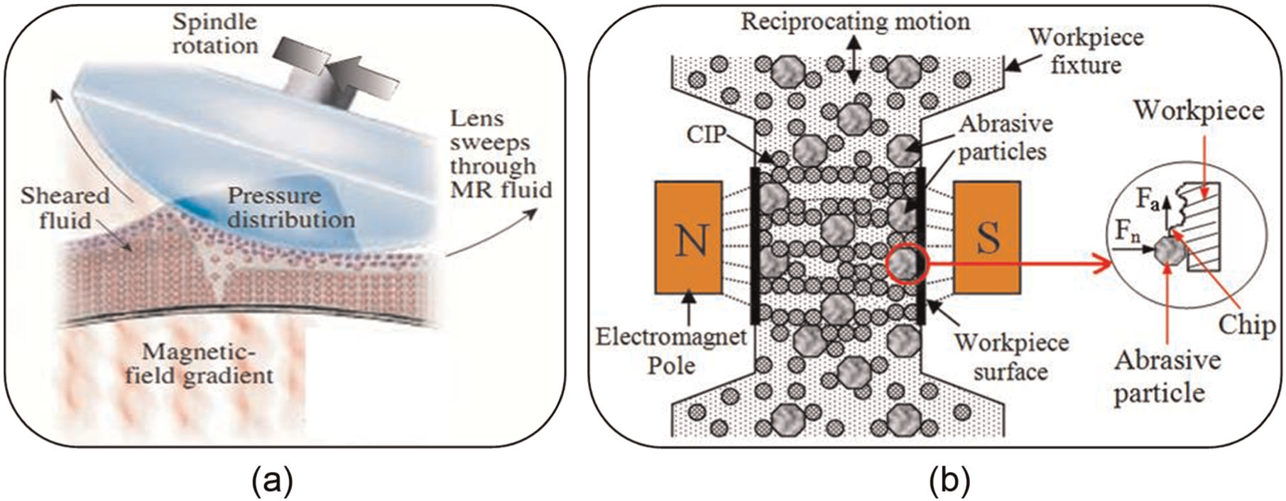
Schematic diagram of (a) MRF process and (b) MRAFF process.
The magnetic field and percentage concentration of magnetic particles in MR fluid mainly decide the strength of MR effect. The theory of magnetic levitation force (Fml) proposed by Rosensweig 108 is used for simulating the behavior of abrasive particles (non-magnetic body) in MR fluid or ferrofluid, and it is defined by
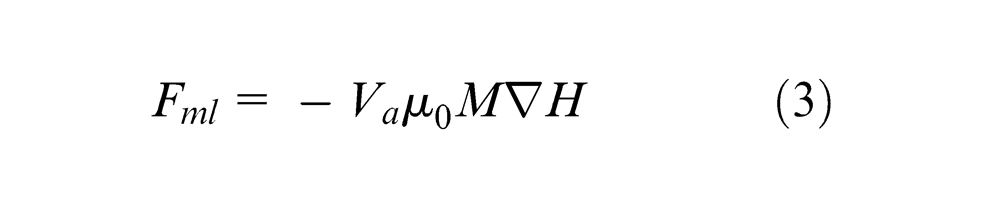
where Va is the volume of non-magnetic body (or non-magnetic abrasive particle (NMAPs)), M is the intensity of magnetization of magnetic fluid, μ0 is the permeability of free space and
However, MRF process has shape constraint, and very hard materials cannot be finished by this process. In case of AFM process, the forces cannot be controlled externally. Hence, by combining these two processes, a new process named as “MRAFF” was developed. 107 Figure 9(b) shows a schematic diagram of MRAFF process where MR fluid is extruded through the cylindrical workpiece or fixture. When magnetic field is applied, MR fluid gets locally stiffened and active abrasive particles in contact with workpiece surface perform finishing. Effectiveness of the MRAFF process can be increased by giving rotation to the magnets (electromagnets or permanent magnets), which increases contact area between abrasive particles and workpiece surface to be finished. This process is named as rotational–magnetorheological abrasive flow finishing (R-MRAFF). 109 MR fluid can also be rotated by automatically changing the magnetic poles in electromagnet at a predefined but short interval. This will produce similar effect as R-MRAFF. In case of MRAFF and R-MRAFF processes, computational fluid dynamics (CFD) and mechanistic approach are used to analyze and simulate the processes in terms of surface roughness, shear stress, forces acting on workpiece surface, distribution of magnetic flux density, flow behavior of MR fluid and so on.109–112
Location of workpiece with reference to the magnet decides the force exerted by abrasive particle on workpiece surface. Figure 10(a) shows the MR fluid located in between the magnet and workpiece. In such situation, the abrasive particles located near workpiece surface play a major role in finishing, while others that are trapped in between magnetic particles’ chains hardly play any role in finishing. The magnetic levitation theory 108 is mostly used for calculation of normal force applied by abrasive particle on the workpiece. Figure 10(b) shows a workpiece located in between MR fluid and the magnet. In this configuration, abrasive particles located far away from the magnet do not play any role in finishing. Only those abrasive particles that are trapped in the magnetic particles’ chains and touch workpiece surface can contribute toward finishing of workpiece surface. The FR is quite low in this case as compared to the earlier case (Figure 10(a)). The force acting on the magnetic particles due to magnetic field is given by Stradling 113
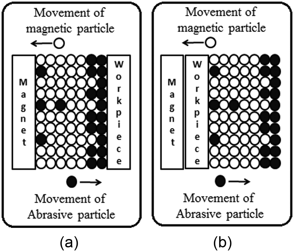
Location of workpiece with reference to the magnet: (a) magnetic fluid in between magnet and workpiece (in case of MRF, MFP processes) and (b) workpiece in between magnet and magnetic fluid (in case of MRAFF process).
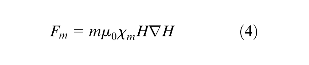
where m is the mass of a magnetic (Fe) particle, χm is the mass susceptibility of the magnetic particle, H is the magnetic field intensity,
Modeling of these processes usually includes analysis of forces acting on workpiece surface, material removal, surface finish and FR. Many researchers have developed theoretical models of surface roughness by calculating forces acting on a single abrasive particle in contact with the workpiece. MRF is a well-established process for finishing or figure correction of glass and optical materials. 114 The chemistry of MR fluid, properties of glass substrate, abrasive particles, abrasion mechanics, shear stress and so on are important parameters to understand the MRF process. 115
A theoretical model was developed 116 for estimating forces acting on a flat surface and the effect of concentration of abrasive particles using two different theories. Furthermore, theory of rolling process was used to calculate squeeze force acting on the workpiece during finishing. Similarly, Sidpara and Jain 117 developed theoretical models for forces acting on freeform surface in MR fluid–based finishing process. It is concluded that angle of curvature of surface has significant effect on the forces due to reduction in effective contact area of finishing spot of MR fluid. Analysis of forces on freeform surfaces is very important in selection of process parameters while finishing complex surfaces like medical implants. A semicircular flexible brush of MR fluid is used for finishing of complex freeform surface of a knee joint implant (Figure 11). 118 Different types of MR fluid and stepwise finishing were proposed to achieve surface finish in nanometer range. A mathematical model was developed 119 for magnetic field–induced normal force in ball end MRF process. The mechanism of material removal was explained by two-body and three-body abrasion of workpiece surface.
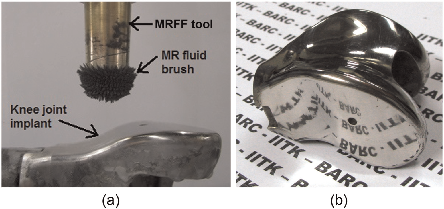
(a) MR fluid brush formation on MRFF tool. (b) Finished knee joint implant by MRFF process.
When it comes to nanometer- or sub-nanometer level finishing, material is removed at atomic level or very near to that, and it is difficult to understand the mechanism of material removal by means of FEM or similar other analytical tools. MDS is effectively used to study abrasive particle–based finishing processes at molecular level.120–123 MDS is extensively used for understanding chemical–mechanical interaction in CMP between abrasive particles and silicon surface.124–126 Therefore, application of MDS for MRF, MRAFF and allied processes will help in better understanding these processes. To understand chemical–mechanical interaction by means of MDS seems to be a future research direction, and it will certainly enhance the understanding of the science involved in nanofinishing.
Deep X-ray lithography
A brief review of usefulness of X-ray lithography (XRL) techniques for HAR microstructures and devices in polymers is presented. The strengths of this technique and main application areas are discussed with the help of a few representative product examples, manufactured by deep X-ray lithography (DXRL) beamline at Indus-2, Raja Ramanna Centre for Advanced Technology (RRCAT), Indore, India.
Microsystem design and developments are driven by the requirements of better device performance, faster response and low fabrication cost. Application-specific microsystems are fabricated by either a single step process or a combination of various microfabrication techniques. The known fabrication techniques in this regard are X-ray LIGA, deep reactive ion etching, electron beam lithography, CNC machines, wet silicon bulk micromachining, UV photolithography, UV LIGA, ultrasonic cutting, excimer laser ablation, EDM and laser cutting. 127 Conventional UV photolithography is almost exclusively used in silicon-based electronics to produce submicron features. However, microsystem requirements are not limited to the smaller features that are routinely obtained in silicon but also require HAR structures in variety of materials. The discussion here is limited to the subject of DXRL and X-ray LIGA, which are used for HAR microfabrication. LIGA is a German acronym that refers to lithography (Lithographie), electro-deposition (Galvanik) and molding (Abformung). X-ray LIGA combines processes of DXRL, electroforming and molding for batch fabrication of HAR microstructures in polymer (resist), metal and ceramic with unprecedented precision and accuracy over a large area. The core process for X-ray LIGA is XRL using synchrotron radiation source. A review of these processes and a wide range of structural devices fabricated for various applications have been discussed Malek 128 and Malek and Saile. 129 Various steps involved in X-ray LIGA process are shown schematically in Figure 12 using “RRCAT” word as an example. In a typical X-ray LIGA process, a required resist master is produced using X-ray exposure of X-ray mask and X-ray-sensitive resist bonded to the conducting base plate (Step 1) followed by developing the resist in a suitable organic developer (Step 2). The resist master on metal substrate is used in the next step for metal electro-deposition such as Ni, Cu, NiW and NiFe. Now, the resist is removed easily to leave the stand-alone metal structure and is shown in Step 4. The last step shows the released polymer structure after hot injection molding process.
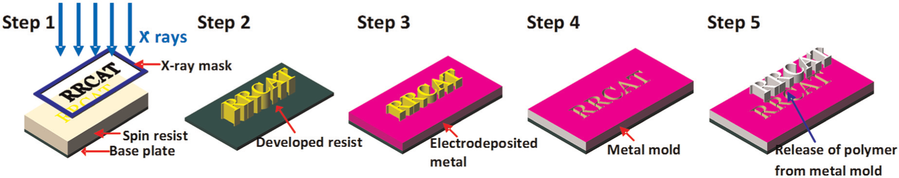
Elemental steps involved in X-ray LIGA fabrication process.
A comparison between X-ray LIGA and various other technologies used for HAR structures are summarized in Table 1. X-ray LIGA offers higher aspect ratio and steep sidewall with lower surface roughness compared to the competing technologies.
Comparison of various tools for microfabrication of high aspect ratio mold.
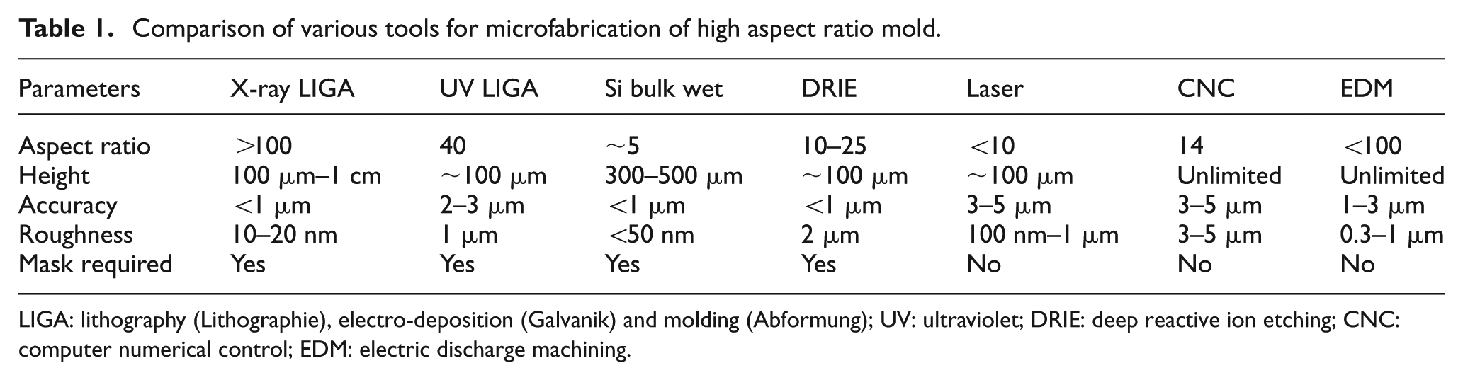
LIGA: lithography (Lithographie), electro-deposition (Galvanik) and molding (Abformung); UV: ultraviolet; DRIE: deep reactive ion etching; CNC: computer numerical control; EDM: electric discharge machining.
Process description of XRL
XRL is a unit magnification shadow printing process and uses X-ray beam from synchrotron radiation source to produce aerial image of X-ray mask for recording a latent image on X-ray-sensitive photoresist. High intensity and low divergence of X-rays from synchrotron source allow high-resolution fabrication due to reduced diffraction effects and taller structures due to higher penetration power of X-rays.
A typical XRL setup consists of a beamline and an exposure system. A synchrotron beamline offers selected X-ray energy spectra using X-ray mirrors 130 or a white X-ray beam without spectrum filtering by X-ray mirror. 131 The X-rays of suitable energy are used for the exposure of resist, up to a thickness of several millimeters. Exposure system consists of a suitable mechanical assembly for mounting X-ray mask and resist. This assembly scans in the vertical direction with suitable scanning rate delivering appropriate exposure dose to the resist without deteriorating the microfeatures. X-ray exposures and development of microstructures at higher energies (>4 keV) known as DXRL allow microfabrication with aspect ratio greater than 100. Shorter wavelength of X-rays reduces diffraction effects and thus allows fabrication of high spatial resolution structures. Resist exposure using hard X-rays is independent of substrate reflection, wafer tomography, substrate type and low atomic number dust contamination, leading to higher reproducibility of the process. Varieties of 3D microstructures are fabricated by giving inclined exposures to resist. 132 Desired dose variation is also demonstrated by giving relative movement to mask and resist with specified speeds 133 or using gray-scale X-ray mask. 134 Projection lithography in hard ray range is not possible due to unavailability of wide-range X-ray demagnification lenses.
Resist
X-rays on interaction with X-ray-sensitive resist introduce chemical changes in it. These radiological changes in the exposed area cause reduction in overall molecular weight of polymer through scissioning, or increase molecular weight of polymer by cross-linking of the monomers. Therefore, the selective dissolution of exposed (positive resist) or unexposed (negative resist) area in suitable organic developer is feasible for the creation of microstructure. X-ray-sensitive resist for X-ray LIGA should have higher sensitivity toward the wide range of X-ray wavelengths, high contrast between the exposed and unexposed region, higher radiation resistance, compatibility with electroforming process and good thermal and mechanical properties. PMMA and SU-8 are the most commonly used as X-ray-sensitive photoresist. PMMA has high contrast, and it is available in solution form or as precast sheet from various suppliers worldwide while SU-8 is available in solution form. Both the resists are used with thickness up to a few millimeters. The lower molecular weight of PMMA due to X-ray exposure is easily dissolved in organic developer solution. These developers should be able to produce HAR and non-tapered structures. Therefore, it is necessary to provide developer at deep recesses and understand surface dissolution kinetics. With increase in aspect ratio and decrease in lateral dimension, the structure may collapse during development due to surface tension and capillary effects. This has been overcome by super critical rinsing and drying in carbon dioxide. 135 Submicron structures and surface roughness of <20 nm have been demonstrated in PMMA using XRL. 136 The resolution is strongly dictated by the molecular weight and energy used for exposure dose. The major drawback of PMMA as an X-ray resist is low sensitivity and susceptibility to cracks due to internal stress. 137 To speed up the throughput, a negative resist commercially known as SU-8 available from MicroChem Corporation, USA, is used for faster development of structures. SU-8 is hundred times more sensitive than PMMA and available in various percentage of solid contents for obtaining resist thickness from 1 to 1000 μm. The limitation of SU-8 is lower resolution, higher tensile stress and difficulty in removal after exposure and hard bake. There is no damage due to bubbles or foaming or swelling observed under high radiation dose. Chemically amplified resist SU-8 on interaction with X-rays generates photoacid. This acid acts as a catalyst to enhance cross-linking of SU-8 monomers in the exposed area. However, the exposure is not sufficient to complete cross-linking and SU-8 is post-baked to generate photoacid to complete the polymerization process. The baking temperature and time depend on the thickness of the resist layer. SU-8 polymer is highly radiation resistant and chemically inert. A review on SU-8 is presented by Del Campo and Greiner 138 for HAR microstructures. The effects of nonuniform dose deposition and beam hardening as a function of depth in the resist, on factors such as surface roughness and sidewall taper, have been studied by Vora et al. 139 PTFE commonly known as Teflon is an interesting material for chemical, biochemistry, electronics and environmental applications. However, the conventional mechanical and molding processes such as micro EDM or injection molding are inadequate for PTFE microfabrication. Direct photo etching of PTFE using high-energy X-rays has opened up new applications of LIGA. 140
Mask
X-ray mask is the most critical component for performing XRL. It consists of X-ray-absorbing high atomic number (Z) material (e.g. Au, Pt, W, Ta) on a X-ray transparent ultra-thin membrane made of low Z material (e.g. C, Ti, Si, SiC, polyimide, BN, Be). The critical dimension of the absorbing pattern can range from submicron to a few tens of microns. The design of the mask depends on the X-ray energy used for exposure, fabrication route and critical dimensions required on the mask. The choice of materials for X-ray mask requires good X-ray transparency (>60%) of the supporting membrane, good X-ray absorption contrast (>100), good mechanical and thermal stability to sustain high-energy X-rays, high radiation resistance (∼MJ/cm2) and compatibility for fabrication processes using electron beam or UV-based lithography. The desired pattern is transferred on the resist either through UV lithography or by direct writing a pattern using electron beam, laser beam or collimated X-ray beam. 141 Actual absorber pattern is obtained by depositing or etching the high Z material in the resist-patterned area. X-ray masks made of titanium membrane (∼2 μm) with gold have produced the sidewall surface roughness in the range of 10–20 nm.
The X-ray LIGA process for the fabrication of a component is extremely time consuming and costly. Thus, there is a strong need to follow proper design methodology and apply design rules for reliable and cost-effective fabrication. DXRL simulation software DoseSim 142 and X3D 143 include computation of synchrotron radiation spectrum from bending magnet, the effect of optical properties of materials, exposure time calculation, insertion of mirrors, which modify the X-ray spectrum, secondary effects, Fresnel diffraction and dose deposited under absorber. For wide spread commercialization and standardization of X-ray LIGA products, rigorous metrology needs to be undertaken. Metrology of fabricated microsystem requires special tools. Meyer et al. 144 compared the results of 3D measurements using coordinate measuring machine with 2D measurements using an optical microscope.
The process of XRL has slowed down mainly due to throughput and complexity involved and also due to major developments in competing HAR fabrication technologies. Even after 30 years of active research, viability of X-ray LIGA as a commercial production tool for HAR microfabrication still remains open, although a few products produced by LIGA have been commercially launched. 145
Applications using DXRL
X-ray LIGA has been phenomenal for generating optical elements in infrared, visible and X-ray regions. The X-ray-etched microstructure has vertical sidewalls with surface roughness in the range of 10–20 nm and depth greater than 1 mm with feature resolution accuracies of few microns, which are attractive for optical device fabrication. XRL is used for fabrication of X-ray optics, 146 desktop monochromator, 147 X-ray refractive lenses and X-ray kinoform lenses. 148 Ultra lightweight X-ray micro-pore optics based on MEMS technologies using XRL and electroplating in curvilinear sidewalls through a flat wafer are fabricated and they have been stacked to form the Wolter type I telescope. 149 A static lamellar grating Fourier transform spectrometer is fabricated using modified X-ray LIGA process. This spectrometer holds unique advantages over common Michelson-type spectrometers including high time resolution, speed, compactness and robustness when they have precise HAR structures. A 16-multi-fiber connector for data communication is developed. 150 The master containing grating structures and mirror is prepared using XRL and all optical components are fabricated in a single step using hot embossing or injection molding. 151
X-ray lenses in PMMA and SU-8 are fabricated using XRL. X-ray lens produced in SU-8 material using XRL beamline on Indus-2 is shown in Figure 13(a). Micro focus characterization of these lenses is carried out at Indus-2 source producing a focal spot size of 11 μm. The X-ray lenses are used in various X-ray techniques such as imaging, microfluorescence and microdiffraction.
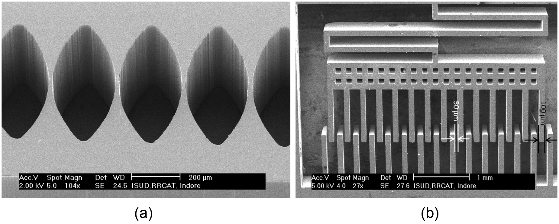
(a) SEM micrograph of SU-8 X-ray lens with geometrical aperture of 400 μm; radius of curvature of lens, 100 μm; thickness of the lens along the optical axis, 15 μm; etched depth, 500 μm. (b) SEM image of a comb-drive structure (depth = 800 μm) made by DXRL, size of each finger is 100 μm and gap between them is 50 μm.
In addition to optical MEMS, microfabrication of MEMS using X-ray LIGA is explored extensively for electrostatic sensors and actuators and radio-frequency microelectromechanical system (RF MEMS). Electrostatic comb-drives are at the heart of many present day’s mechatronic system. Comb-drive works on electrostatic principle and can be used as microactuator, 152 resonator, 153 accelerometer, 154 energy harvester, 155 voltmeter, optical shutters, microgripper and electromechanical filters.156,157 The HAR comb actuators are capable of generating higher force and displacement, useful for high-performance microactuators, micromanipulators and many other micro positioning applications. Figure 13(b) shows a microstructure of a comb-drive fabricated in PMMA by DXRL process at Indus-2. 158 Furthermore, the electrostatic micromotors work as a building block for lab-on-a-chip, microscopy, data storage, optical and biomedical systems. 159
RF MEMS is an emerging field finding applications in mobile phones, wireless data network, global positioning system (GPS), nano-satellites, radio-frequency identification (RFID) tags and sensors. The building blocks of RF MEMS are high-quality factor lumped reactive and tunable reactive elements such as capacitors, varactors and inductors, 160 couplers and power dividers, filters, 161 resonant cavity structure 162 and micromachined transmission lines. 163 Planar structures fabricated in Si are lossy due to low electrical resistivity of Si. RF applications in general require good conductors and vertical sidewall structures. The vertical metal wall RF structures produced by X-ray LIGA limit the losses and increase quality factor at higher frequency (3–300 GHz).
The Micro Harmonic Drive® system provides high reduction ratio, zero backlash, high efficiency and high torque dynamics for faster indexing applications. These systems are highly suitable for precise positioning applications in semiconductor, manufacturing equipment, medical devices, measuring equipment, optical devices, machine tools and spacecraft. 164 X-ray LIGA is used for the production of harmonic drive gear with submicron tolerances and high metallic finish. Collaborative efforts between BESSY AZM and CAMD synchrotron facilities, Micro Resist Technology and Micromotion have produced Micro Harmonic Drive of 4 μm and depth of 1024 μm. 165
In conclusion, professional X-ray LIGA-based microfabrication requires significant infrastructure with clean rooms and equipment, synchrotron-based X-ray beamline, supporting laboratories, X-ray mask making capabilities and highly qualified and trained human resource for operating these facilities. Converting a high-end research to a commercially viable product needs to address issues connected with reproducibility, manufacturability, cost acceptability and collaborative efforts of interdisciplinary fields.
Concluding remarks
From the above review, it can be seen that a gap exists in different micromanufacturing processes in which R&D activities should be concentrated to enhance the product quality and process performance. Also, new areas of the applications of these processes/products should be explored to motivate further R&D activities to lower down the overall cost of the products. Most of the micromanufacturing processes need fundamental research in the design and development of the machine tools for these processes, rather than scaling down the existing machine tools being used for macromanufacturing. The researchers should also aim on how to cut down the cost of product and how to enhance the productivity so that low-cost mass production becomes feasible. Finally, extensive work needs to be done in the area of evaluation of mechanical and physical properties of the micromanufactured products.
Footnotes
Declaration of conflicting interests
The authors declare that there is no conflict of interest.
Funding
This research received no specific grant from any funding agency in the public, commercial, or not-for-profit sectors.