
Abstract
Finishing mirror-like surfaces on chemically vapor-deposited diamond film using an in-process composite electroplating of diamond grains onto the tool surface, the tool can maintain its sharpness in a grinding process. The effect of diamond grit size of the tool on the grinding characteristics of diamond film is investigated. To promote optimum grinding efficiency, a high variation rate in the surface roughness of diamond film and a small growth rate in the coating thickness are desired. A distribution model of the diamond grits in the coating layer is deduced, and a composite electroplating in-process sharpening grinding mechanism is developed using a body-centered tetragonal structure. A two-stage composite electroplating in-process sharpening grinding procedure is used to grind the diamond film. A grit size of 25 µm is selected to conduct the composite electroplating in-process sharpening grinding for 30 min at an initial surface roughness of 1.1 µm. Then, the operating conditions are switched to a grit size of 3 µm and a grinding time of 180 min, and a mirror-like surface on the diamond film with an average surface roughness of 0.03 µm is obtained.
Introduction
Many methods are now used to grow diamond film on a substrate. However, columnar growth of chemically vapor-deposited (CVD) diamond film results in a very rough surface, resulting in limitations on the applications of diamond films. In addition, diamond is the hardest material known and has extremely stable physical and chemical characteristics, so it is very difficult to machine. Diamond machining methods can be roughly classified as mechanical grinding,1,2 thermomechanical polishing,3–6 ion-beam polishing, 7 and laser polishing.8,9 Because the equipment used in mechanical grinding is relatively simple, it is widely used in the polishing of diamond films. Moreover, many modified methods, such as the electronic in-process dressing (ELID) 10 and composite electroplating in-process sharpening (CEPIS), 11 are also used to improve the capability of grinding tools and thus the efficiency of grinding.
In traditional mechanical grinding, the hardness of an abrasive material in a grinding tool is usually higher than that of the workpiece. Hence, the grinding characteristics of the workpiece, such as the surface roughness and the material removal rate (MRR), are easily evaluated when using different grit sizes because the tendency of the grain to fracture is relatively slow. Since diamond film is such a hard material, diamond abrasives are generally used for grinding diamond film. Under this condition, the abrasives and the workpiece have the same degree of hardness, and the effect of the abrasive grit size on the MRR is hard to estimate because the grits are easily made blunt.
The coating thickness on the grinding tool and the removal amount of the diamond film were proportional to the CEPIS grinding time, as reported by Chen et al. 11 This indicated that the sharpness of the grinding tool was maintained so that the grinding tool resharpened by a procedure called dressing could be eliminated. The diamond film could be ground using this method with diamond grit size of 10 µm and grinding time of 15 min to achieve a surface roughness that was superior to that using conventional machining. This result clearly shows that the feasibility of grinding diamond using the CEPIS method to be confirmed. In this study, the CEPIS method is also used to grind CVD diamond films. The effect of diamond grit size of the tool on the grinding characteristics of diamond film is investigated.
Experimental
A schematic diagram of the CEPIS grinding apparatus is shown in Figure 1, and the plating operation is carried out in a nickel chloride electrolyte using the compositions given in Table 1. The plating procedure is described in detail in our previous article. 11 Current density is widely used to estimate the amount of electric current passing through a plating area, and it is measured in amperes per square decimeter (ASD).
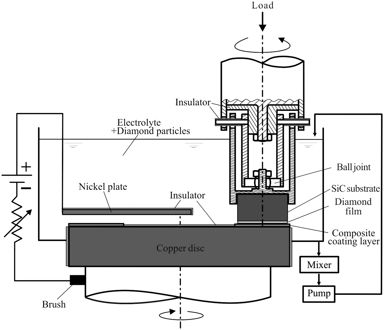
Schematic diagram of the grinding apparatus with composite electroplating in-process sharpening method.
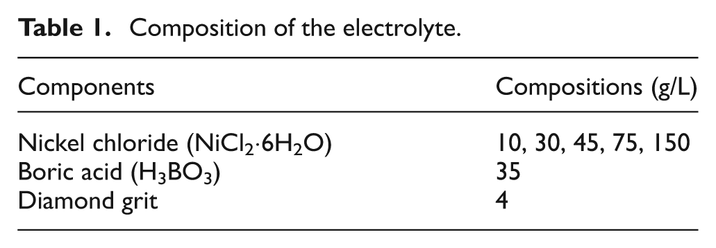
Composition of the electrolyte.
A CVD diamond film with a thickness of 25 µm and a diameter of 20 mm is deposited onto the SiC surface, and its surface structure is columnar with surface roughness Ra of about 1.1 µm, as shown in Figure 2(a). The diamond film is ground to Ra of about 0.2 µm to understand the initial effect of the surface roughness of the diamond film, and its surface structure is shown in Figure 2(b).

SEM micrographs of the CVD diamond film under different initial surface roughness, Ra: (a) 1.1 µm and (b) 0.2 µm.
After the electroplating process, it was found in the earlier study 11 that the operating parameters should be adjusted to minimize the grinding time as presented in Table 2. After grinding, the surface characteristics of the grinding tool and the diamond film are measured and observed by surface profilometer and SEM.
Operating parameters.
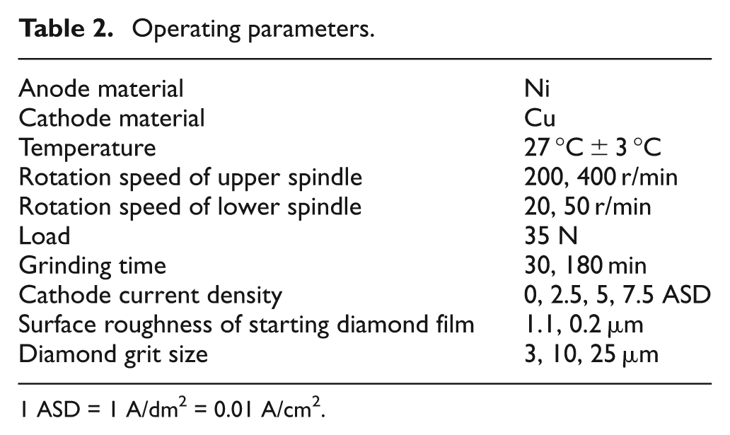
1 ASD = 1 A/dm2 = 0.01 A/cm2.
Results and discussion
Composite electroplating characteristics of the coating layer
Figure 3 shows the variations for the average coating thickness of the grinding tool at a disc speed of 50 r/min and a current density of 7.5 ASD under different diamond grit sizes in the electroplating process. Figure 3 clearly shows that the average thickness of the pure nickel is proportional to electroplating time in the plating bath without diamond grits. After an electroplating time of 30 min, the average thickness of the pure nickel is about 17 µm. This result is in good agreement with Faraday’s law. In addition, the average thickness of the Ni–Diamond composite coating increases from 21 to 52 µm with increase in grit size from 3 to 25 µm after the same electroplating time. Figure 4 shows the SEM micrographs of the coating layer. It makes clear that the diamond grits on the coating layer are uniformly distributed and that the nickel substrates are smoothly deposited using different grit sizes. Figure 5 shows the weight loss of the nickel plate in the anode during the electroplating process. It clearly shows that the weight loss of the nickel plate using different sizes of diamond grits is almost the same as that of pure nickel.
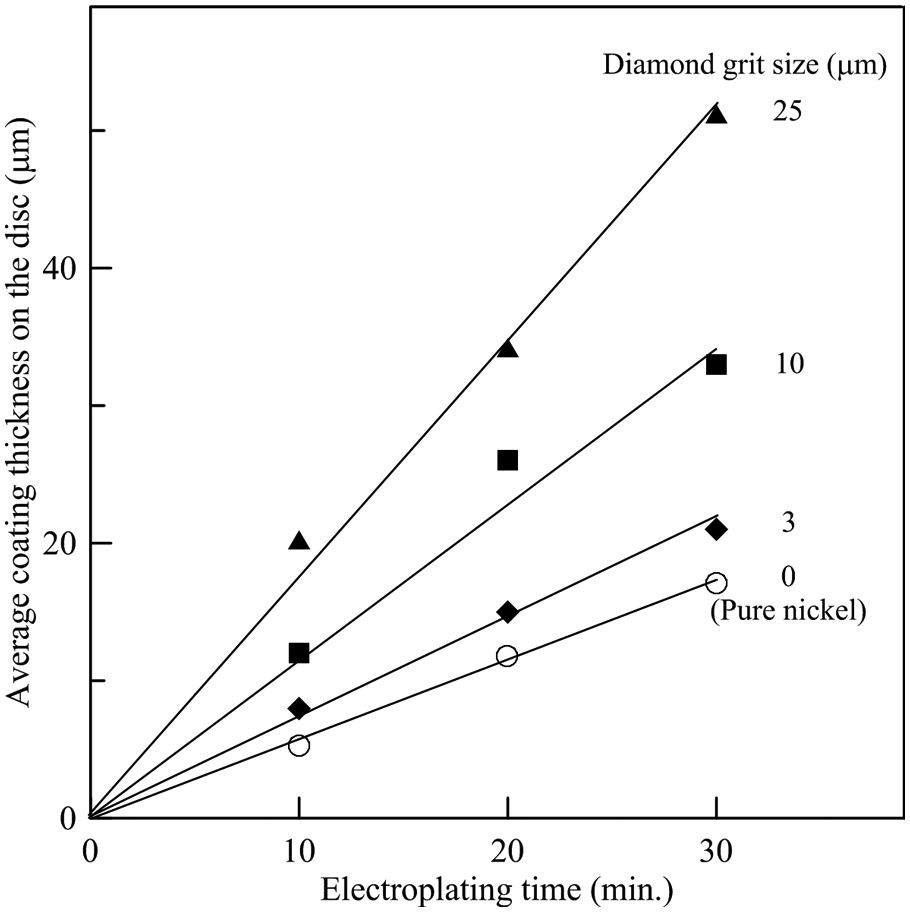
Variations for the average coating thickness on the grinding tool during the electroplating process.

SEM micrographs of the coating layer on the grinding tool under different diamond grit sizes: (a) 3 µm, (b) 10 µm, and (c) 25 µm.
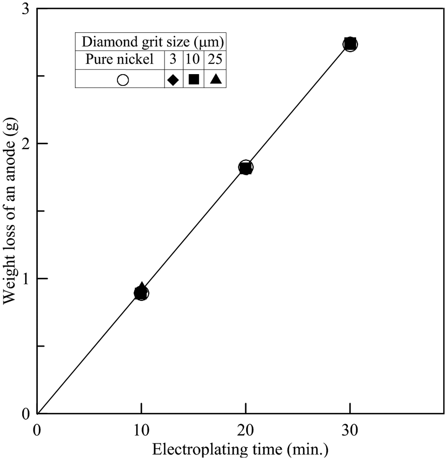
Weight loss of an anode during the electroplating process.
Furthermore, the covered area ratio, η, of the diamond grits to the surface area of the coating layer is estimated using an image analysis method. 11 This method can transform the color of the diamond grits and the nickel base into black dots and a white region, respectively. The variation for the covered area ratio of the diamond grits to the surface area is shown in Figure 6. In Figure 6, it can be seen that this ratio increases rapidly with smaller grit sizes and approaches near saturate value with larger grit sizes. This is because the grit is easily precipitated on the disc using larger grit sizes. Meanwhile, the average thickness of the composite coating increases as the grit size increases.
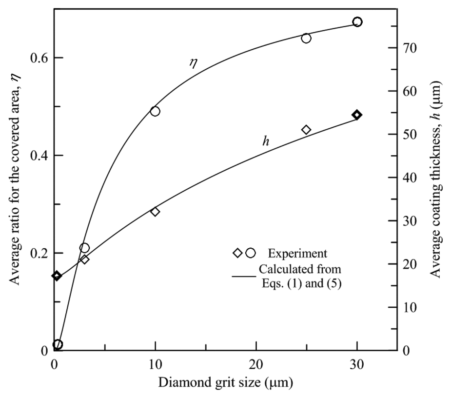
Variation for the covered area ratio of the diamond grits to the surface area and the average coating thickness under different diamond grit sizes.
Distribution of diamond grits on the composite coating layer
Figures 3–6 show that grit size significantly affects the distribution of diamond grits in the composite coating layer. Hence, an attempt is made to determine the effect of diamond grit size on this distribution. The following assumptions are made to simplify the calculation: The composite coating layer consists of diamond grits and nickel substrate only. The diamond grit is considered to be a sphere. The diamond grits are situated in a repeating or periodic array on the coating layer.
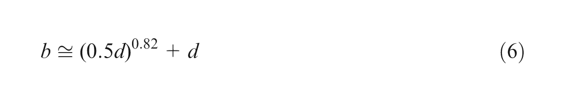
Because the diamond grits are stacked on the disc by deposition in the electroplating process, it is convenient to subdivide the coating layer into small repeated entities. After the numerical trials under the same procedure mentioned in the following, a body-centered tetragonal (BCT) structure per unit cell is selected as the model, as shown in Figure 7(a). In this cell, the grits are located at all eight corners with a single grit in the center. Hence, the edge lengths a and b can be estimated. First, the ratio, η, of the diamond grits to the surface area can be expressed as
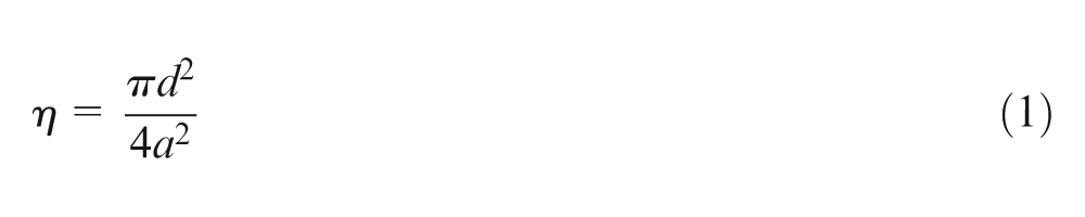
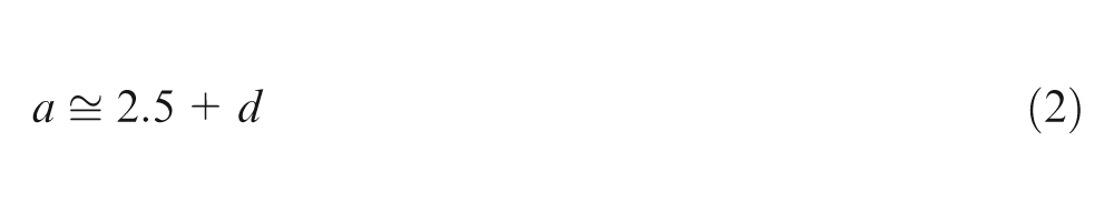
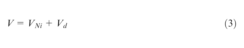
where d is the diameter of the grit and a (µm) is the edge length of the cell or the distance between the center of the two grits in the horizontal plane. For example, Figure 6 shows that η is about 0.498 at the grit size of 10 µm, and a is equal to 12.55 µm from equation (1). After all the data of a are calculated from equation (1), they can be expressed in terms of the diameter of the grit, d, by regression analysis
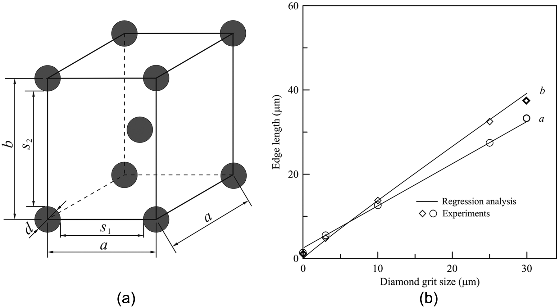
(a) Schematic diagram of the distribution of diamond grits in the Ni–diamond composite coating layer and (b) edge length for the experiments of the BCT unit cell.
The volume, V, of the composite coating layer consists of the volume, Vd, of the diamond grit and the volume, VNi, of nickel substrate. Hence, their relationship in each unit cell can be expressed as
Because the surface area of the disc remains constant, equation (3) is divided by this area to obtain the thickness relationship as
where h is the total thickness of the coating and hNi and hd are the thicknesses contributed by the nickel substrate and the diamond grit, respectively. For the BCT structure, a total of two whole grits may be assigned to a unit cell. Hence, the ratio of the hNi to h can be expressed as
It is also shown in Figure 5 that the thickness, hNi, is independent of the grit size, b (µm) is the edge length of the cell or the distance between the center of the two grits in the vertical plane. Using the experimental data of the average coating thickness shown in Figure 6, the edge length b can be calculated as
Substituting equations (2) and (6) into equations (1) and (5), η and h can be estimated, as shown in Figure 6. Figure 6 shows that the calculated values of η and h are in agreement with the experimental results.
To test the capability of the BCT structural model, five grit sizes are electroplated on the disc. The grit sizes of 0.3 and 30 µm are selected so that the grit sizes are at the extremes of the model. These experiments are made with grit sizes that are outside of those used in creating the model. Figures 6 and 7(b) demonstrate that the model can predict the distribution of diamond grits beyond the initially investigated parameters. This also means that the above-mentioned assumptions are confirmed.
Grinding characteristics of CVD diamond film
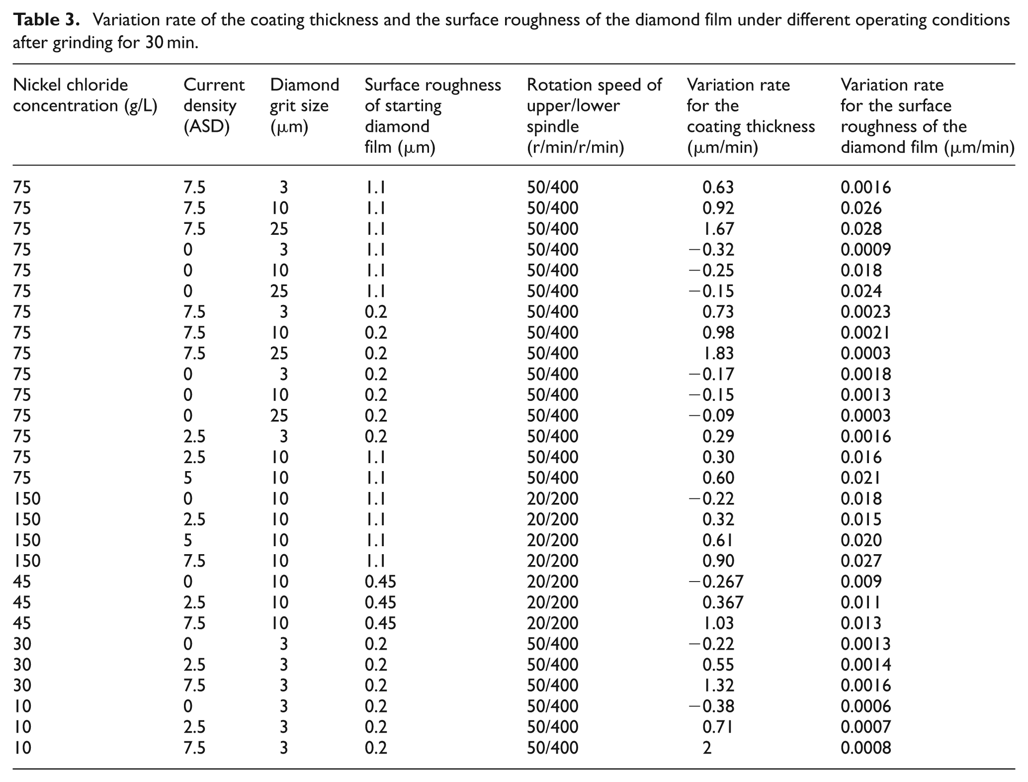
CVD diamond films are ground by composite on a disc; its grinding characteristics are investigated, and the typical results are shown in Table 3. In the traditional grinding process, the MRR is widely used to estimate the grinding efficiency. However, in this study, the MRR is too small (<0.01 mg/min) to be measured during a grinding process at smaller grit sizes. Therefore, the variation rate of the average surface roughness, Ra, of the diamond film is used to estimate the grinding efficiency. Table 3 shows that the variation rate of the coating thickness and the Ra of the diamond film are significantly affected by operational conditions. Basically, a high variation rate in the roughness of diamond film and a small growth rate in the coating thickness are desired. The effects of the operational conditions on both variation rates are outlined below.
Variation rate of the coating thickness and the surface roughness of the diamond film under different operating conditions after grinding for 30 min.
Concentration of the nickel chloride
The concentration of the nickel chloride can influence the structure of the composite coating in the CEPIS process. The coating structure is looser, and a “cauliflower” structure is formed by microcrystalline aggregates at a nickel chloride concentration of 10 g/L. Furthermore, these agglomerates are characterized with the presence of pores, and the composite coating is loosely stacked at lower concentrations. Hence, the growth rate for the coating thickness is higher, and the corresponding coatings have poor mechanical properties. Under these conditions, the variation rate of the roughness of the diamond film is poor. The size of microcrystalline aggregates decreases with increasing concentrations of 30 g/L or higher, so that “ball-like” agglomerates and fine-grained, compact deposits are formed. These corresponding coatings have better mechanical properties. Hence, a lower growth rate for the coating and a higher variation rate for the roughness are obtained. When the concentration is larger than 75 g/L, the limiting current density of the electrolyte is increased. This means that the electrolyte can maintain stability and that the coating layer can remain compact at higher current densities in the CEPIS process.
Current density
In the CEPIS process, the current density is the most important parameter because it can directly determine the deposition rate of the coating layer. The variation rate of the coating thickness is negative with no electricity. However, the variation rate for the coating thickness is positive at current densities of 2.5, 5, or 7.5 ASD. Meanwhile, the variation rate of the diamond film surface roughness is also increased. These results clearly show that the coating thickness of the grinding tool can be maintained or slightly increased, and its sharpness is also renewed in the CEPIS grinding process, leading to a higher variation rate in the diamond film surface roughness during the grinding process. When the current density is larger than 7.5 ASD or exceeds the limiting current density of the electrolyte, a looser “cauliflower” structure may be formed.
Diamond grit size and Ra of the initial diamond film
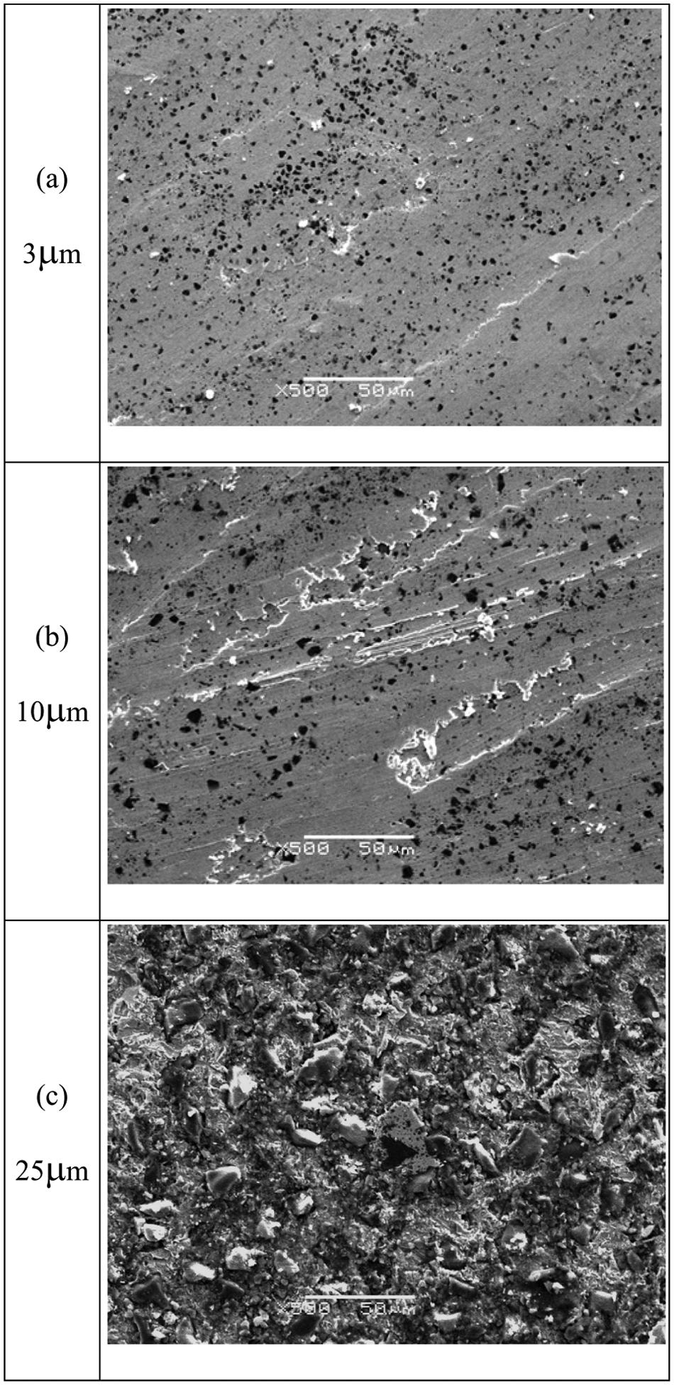
In this study, both abrasive grit and the workpiece have the same hardness, and it can be considered that they can be ground by each other. To determine which one is treated as the “tool” and which as the “workpiece” in the grinding process, the relationship between diamond grit size and the roughness of the initial diamond film plays an important role. Figure 8 shows the thickness variations for the composite coating on the grinding tool under different degrees of surface roughness in the initial diamond film and diamond grit sizes in the CEPIS grinding process. Figure 8 makes clear that the average coating thickness increases with increase in grinding time. These initial degrees of surface roughness have a roughness of 0.2 µm for the smoother diamond film and 1.1 µm for the rougher diamond film. The growth rate of the coating increases with increase in grit size, and a higher growth rate is obtained when smoother diamond film is ground. Moreover, the coated structures on the grinding tool can be observed using a scanning electron microscope. Figure 9 shows typical SEM micrographs of the coated surface under different degrees of surface roughness for the initial diamond film and grit sizes, and it is shown to be significantly different from the initial coating (Figure 4). In Figure 9, the grit sizes almost remain the same, and no obvious scratches are observed under different grit sizes after a CEPIS grinding process of 30 min. In addition, some agglomerates of the nickel and diamond are observed on the coating surface under rougher and smaller grit size conditions. The agglomerates become smaller with increasing grit size and decreasing initial surface roughness. Figure 10 shows Ra of the diamond film versus the grinding time. Figure 10 makes it clear that the diamond film can be efficiently ground using larger grit sizes on a rougher diamond film, but it is barely ground on a smoother diamond film.
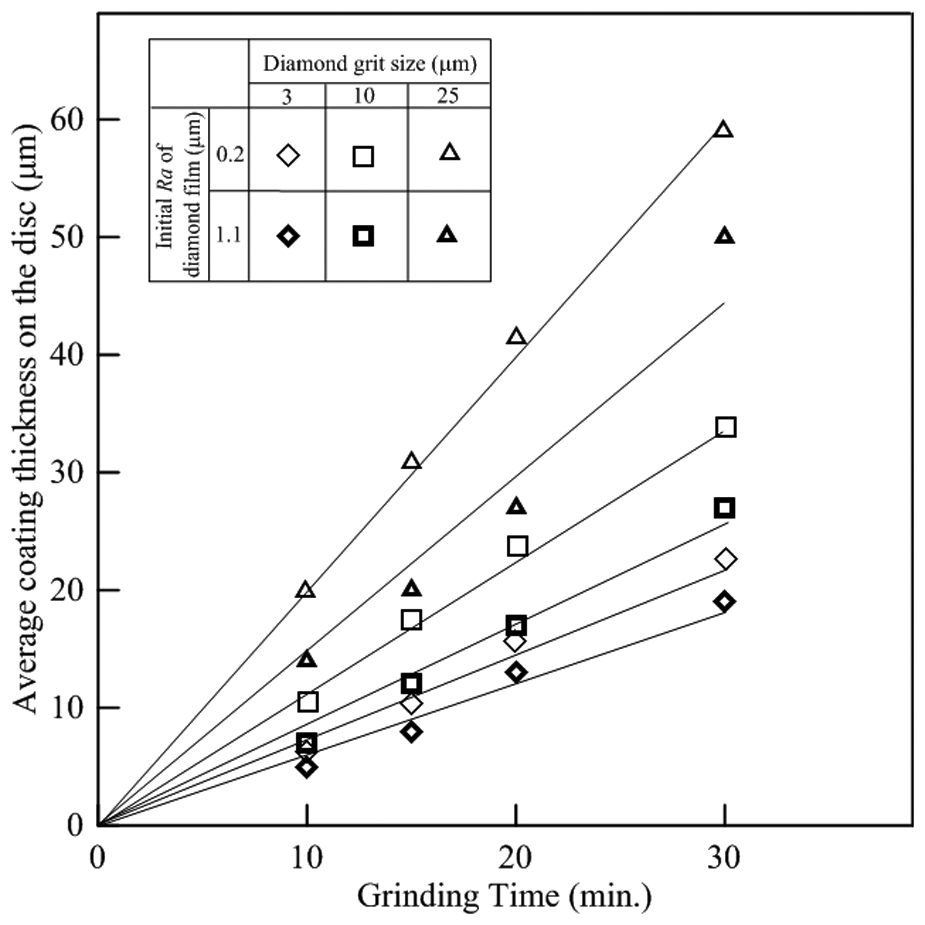
Thickness variations for the composite coating on the grinding tool under different degrees of surface roughness in the initial diamond film and diamond grit sizes in the CEPIS grinding process.
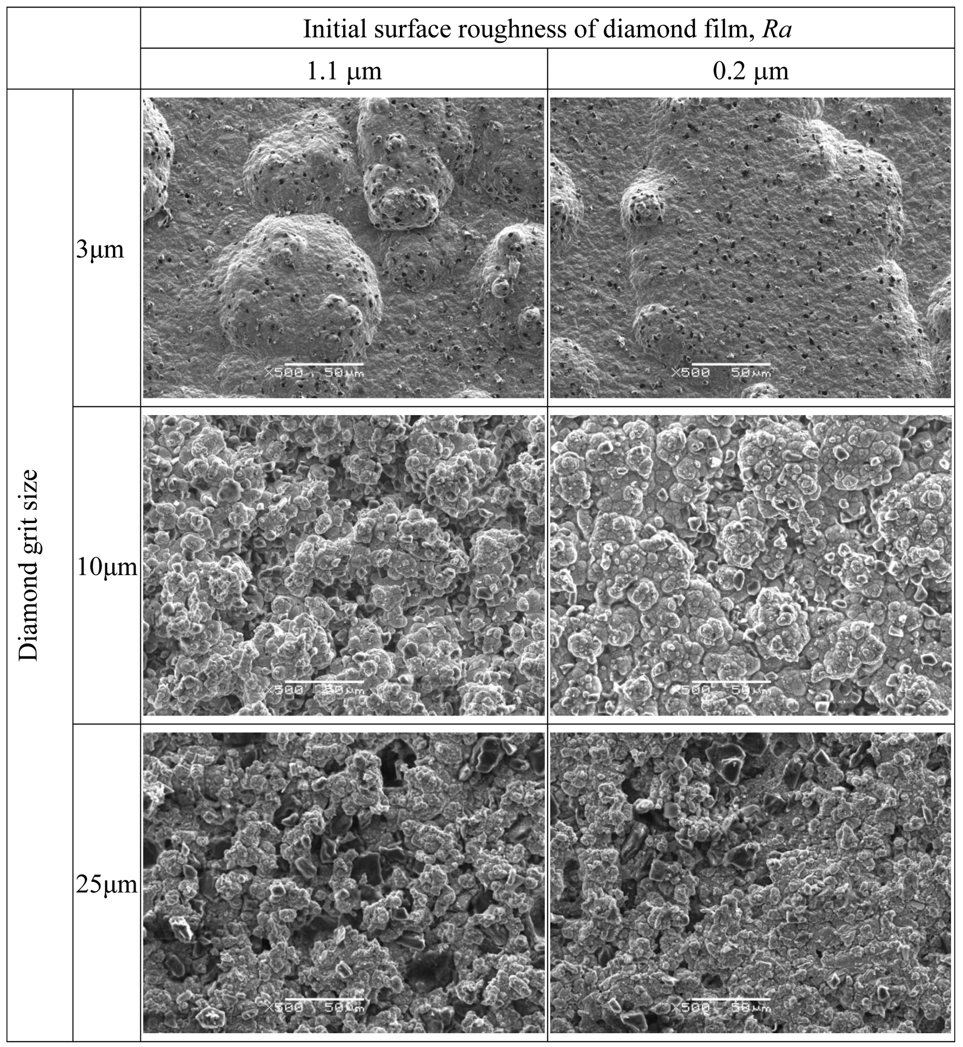
SEM micrographs of the coating layer on the grinding tool under different initial surface roughness of diamond films and diamond grit sizes: (a) 3 µm, (b) 10 µm, and (c) 25 µm.
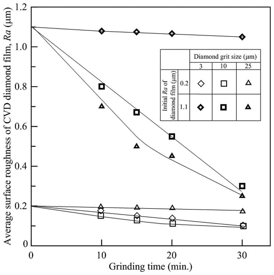
Variation for the average surface roughness of the diamond film under different initial surface roughness of diamond films and diamond grit sizes.
To determine the contact behavior between diamond film and composite coating under different grit size conditions, the diamond film is ground with no electricity. The variation rate of the coating thickness decreases with increase in grit size. This means that the coating is rapidly worn away at a smaller grit size. In addition, the SEM micrographs of the composite coating after the grinding time of 30 min are also observed, as shown in Figure 11. It can be seen that the angle of the tip of the column in the diamond film remains in the range of 85°–105°, as shown in Figure 2(a), and the gap between diamond grits on the coating in the horizontal plane remains constant, as shown in equation (2). Hence, the contact behavior is only affected by the diamond grit size. Figure 11 clearly shows that the columns are easily in contact with the nickel substrate of the coating layer through the gap between the grits at a grit size of 3 µm. Hence, both nickel substrates and diamond grits are easily removed by diamond film, as shown in Figure 11(a). In this condition, the roughness of the diamond film varied a little so that it can be treated as the “tool” and the coating as the “workpiece.” When the grit size increases to 10 µm, the columns can partially penetrate the gap between the grits, and then, the diamond grits can sustain these columns, so that these columns are relatively difficult to be in contact with the nickel substrate, as shown in Figure 11(b). In this condition, the variation rate of the roughness on the diamond film is significantly increased, and it can also be considered that both the diamond film and the coating are ground by each other. As the grit size increases to 25 µm, the columns are only in contact with the diamond grit, as shown in Figure 11(c). Hence, the diamond film is treated as the “workpiece” and the coating as the “tool.”
SEM micrographs of the composite coating after grinding for 30 min at the current density of 0 ASD under different particle sizes: (a) 3 µm, (b) 10 µm, and (c) 25 µm.
CEPIS grinding mechanisms
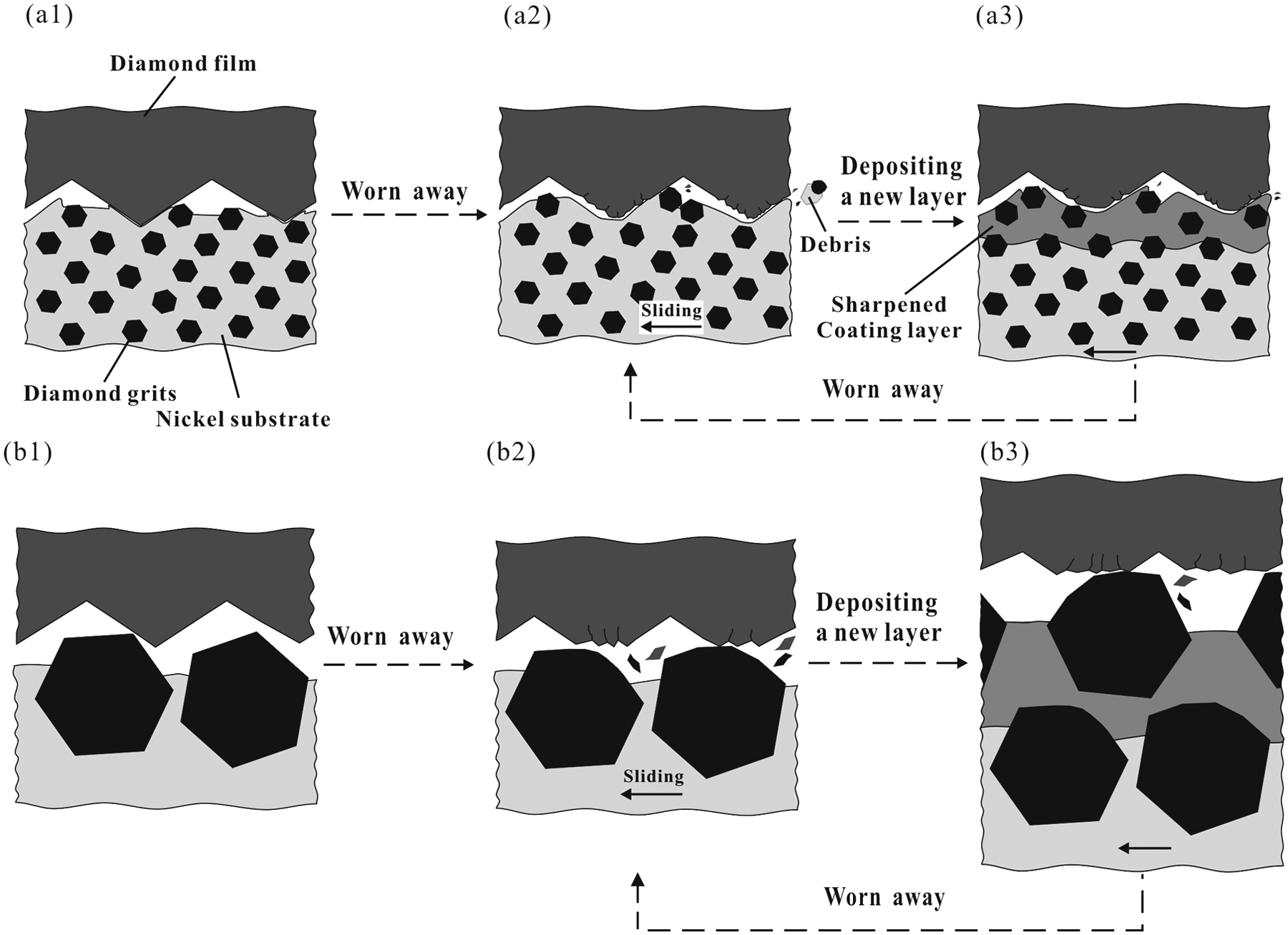
In light of the aforementioned results, the CEPIS grinding mechanisms under different grit size conditions are shown in Figure 12. When the diamond grit size is smaller than the column size in the diamond film surface, the column can directly penetrate the nickel substrate (Figure 12(a1)). The coating layer containing diamond grits is removed from the grinding tool surface during the grinding process (Figure 12(a2)). Although the coating layer is renewed using the composite electroplating method, and the new diamond grits possess new cutting edges on the grinding tool, this new layer is still easily removed by the columns in the diamond film surface. Hence, the grinding ability of the grinding tool becomes worse, and the roughness of the diamond film slowly decreases (Figure 12(a3)). When the grit size is larger than the column size in the diamond film surface, the column contacts the diamond grit, but it is difficult to penetrate the nickel substrate on the grinding tool (Figure 12(b1)). The column is rapidly removed during the grinding process (Figure 12(b2)). When the diamond grits are worn away, the coating layer in the grinding tool is renewed using the composite electroplating method so that the sharpness of the coating layer is maintained. Hence, the roughness of the diamond film decreases rapidly (Figure 12(b3)).
The CEPIS grinding mechanisms under different grit sizes: (a) when the diamond grit size is smaller than the column size on the diamond film and (b) when the diamond grit size is larger than the column size on the diamond film. The marks 1, 2 and 3 represent contacting, grinding, and sharpening process, respectively
Grinding CVD diamond film using two-stage process of the CEPIS
As mentioned above, it can be seen that the diamond film can be efficiently ground using larger grit sizes on a rougher diamond film but is barely ground using a smoother one. Hence, the two-stage CEPIS grinding procedure has to be adopted. In the first stage, the roughing operations are carried out at a large grit size. Second, the finishing operations are carried out at a small grit size.
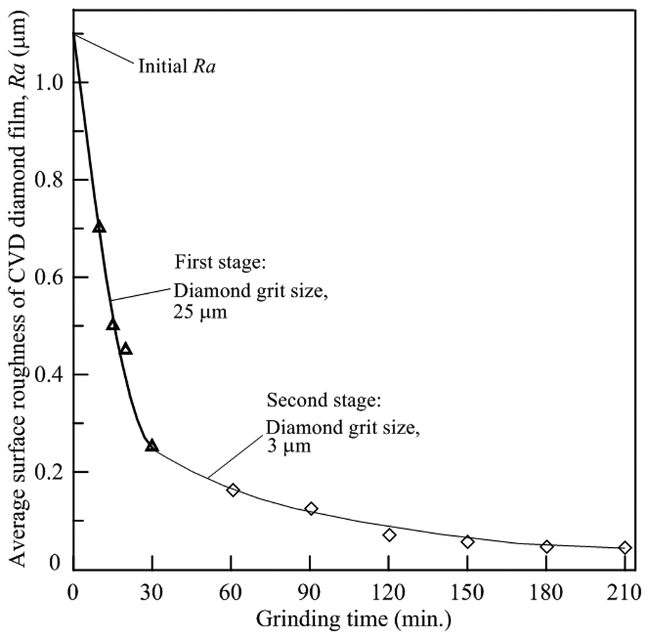
Figure 13 shows the variations for Ra of the diamond film at a load of 35 N, a disc speed of 50 r/min, and a workpiece speed of 400 r/min. First, the grit size of 25 µm is selected to conduct the CEPIS grinding for 30 min at an initial surface roughness of 1.1 µm. Then, the operating conditions are switched to a grit size of 3 µm. Finally, the average surface roughness of the diamond of 0.03 µm is obtained using a two-stage CEPIS grinding process. Figure 13 clearly shows that the rougher surface of the diamond film can be efficiently ground using this two-stage process of the CEPIS.
Variations for the average surface roughness of the diamond film at a disc speed of 50 rpm, a workpiece speed of 400 rpm using a two-stage CEPIS grinding process.
Figure 14 shows the SEM micrographs of the CVD diamond film using the two-stage CEPIS grinding method after a grinding time of 210 min. Compared with the initial diamond film (Figure 2(a)), the columns on the diamond film are shown to be removed, and a mirror-like surface is obtained after the two-stage process.
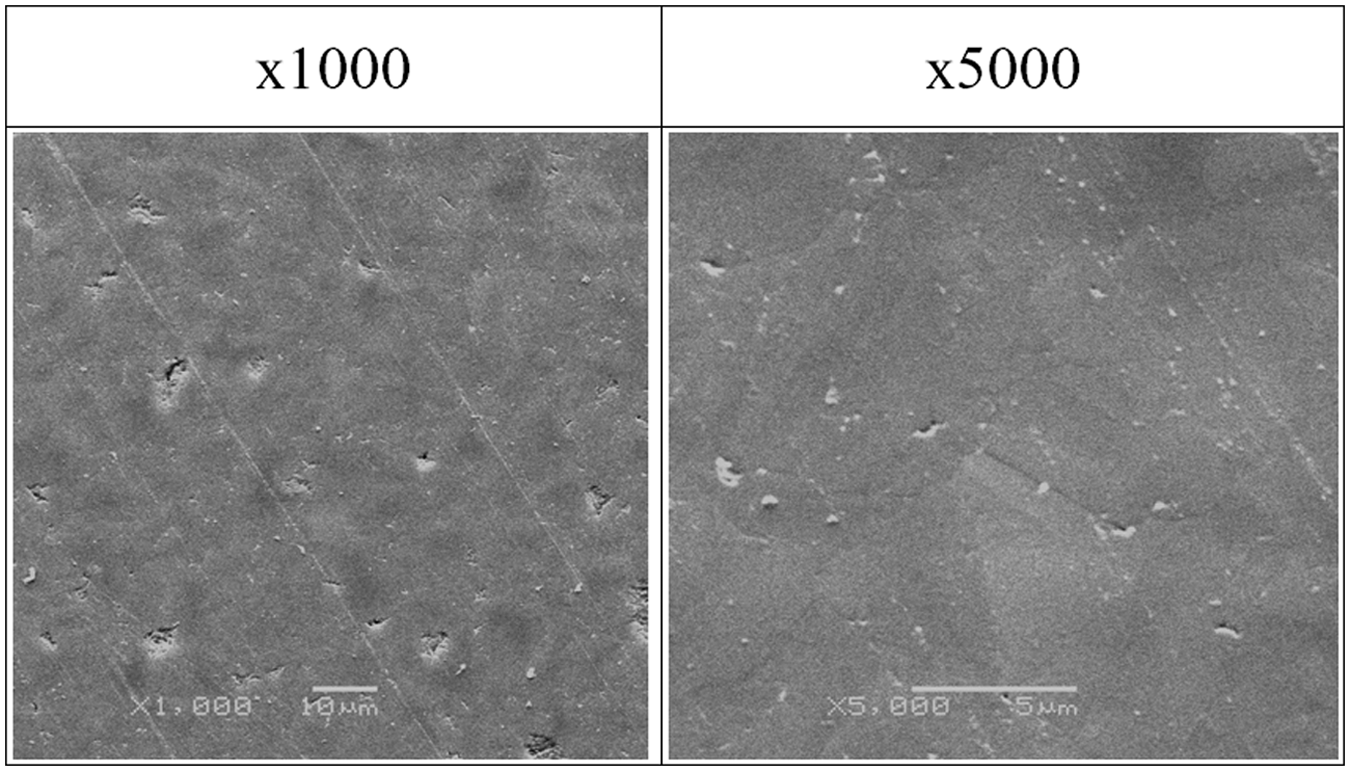
SEM micrographs of the CVD diamond film at a grinding time of 210 min.
Conclusion
CVD diamond film is ground using a CEPIS method. The effect of diamond grit size of the tool on the grinding characteristics of diamond film is investigated. Based on the experimental results, the main findings are outlined as follows:
To promote optimum grinding efficiency, a high variation rate in the surface roughness of diamond film and a small growth rate in the coating thickness are desired. To meet this demand, a current density is in the range of 2.5–7.5 ASD, a concentration of nickel chloride is in the range of 30–150 g/L, and the diamond grit size is larger than the column size on a diamond film surface.
A distribution model of the diamond grits in the coating layer is deduced, and a CEPIS grinding mechanism is developed using a BCT structure.
The diamond film treated as the “tool” can grind the composite coating at a smaller grit size because the columns can directly contact the nickel substrate on the coating through the gap between the grits. Hence, the coating rapidly wears away. The columns are only in contact with the diamond grit at larger grit size. Hence, the diamond film treated as the workpiece can be ground efficiently.
A two-stage CEPIS grinding procedure is used to grind the diamond film. A grit size of 25 µm is selected to conduct the CEPIS grinding for 30 min at an initial surface roughness of 1.1 µm. Then, the operating conditions are switched to a grit size of 3 µm and a grinding time of 180 min. Finally, a mirror-like surface on the diamond film with an average surface roughness of 0.03 µm is obtained.
Footnotes
Acknowledgements
The authors would like to express their appreciation to the National Science Council (NSC-95-2221-E-110-007-MY2) in Taiwan for financial support.
Conflict of interest
The authors declare that there is no conflict of interest.
Funding
This research received no specific grant from any funding agency in the public, commercial, or not-for-profit sectors.