
Abstract
Based on a well-designed growth procedure, a tri-material, namely, a three-layer boron-doped micro-crystalline, undoped micro-crystalline and undoped nano-crystalline composite diamond film, is deposited on the pretreated WC–6 wt% Co substrate, the basic characters of which are systematically studied and compared with some other commonly used diamond films. Besides, the growth times for three respective layers are accordingly determined. It is further clarified that the underlying boron-doped micro-crystalline diamond layer can well adhere to the WC–Co substrate due to either the reduction in the residual stress or the formation of B–Co compounds. There is no doubt that the surface undoped nano-crystalline diamond layer with relatively lower hardness and initial surface roughness is more convenient to be polished to the required surface roughness. Moreover, when the growth times for the middle undoped micro-crystalline diamond layer and the surface undoped nano-crystalline diamond layer are both appropriate, the undoped micro-crystalline diamond layer with extremely high diamond quality and hardness can effectively reinforce the surface hardness of the whole composite film. Based on the discussions on the influences of the growth times for the different layers on the performance of the composite diamond film, the growth times for the boron-doped micro-crystalline diamond, undoped micro-crystalline diamond and undoped nano-crystalline diamond layers are, respectively, determined as 4, 4 and 2 h. Under such conditions, the reinforcement effect of the middle layer on the surface hardness can be guaranteed, and the undoped nano-crystalline diamond grains have totally covered the undoped micro-crystalline diamond layer.
Introduction
Chemical vapor deposition (CVD) diamond films have extremely high hardness, high wear resistance and relatively low frictional coefficient, making them potential protective coatings on working surfaces of various wear-resistant and anti-frictional components widely used in the mechanical engineering, such as drawing dies, pivotal components used in metal cold-drawing processes; 1 cutting tools, consumables that are easy to wear in material machining processes;2,3 together with some other important mechanical parts. 4 Deposition technologies adopted for synthesizing CVD diamond films involve the microwave plasma CVD (MPCVD), hot filament CVD (HFCVD), direct current (DC) plasma jet CVD (DPJCVD) and combustion flame CVD (CFCVD), among which the HFCVD technology has attracted the most interests due to its advantages like the geometrical simplification, low cost and operational convenience, together with the practicality on complicated, large-area and inner hole surfaces. 5
The frictional performance, wear resistance and the working lifetime of diamond-coated wear-resistant and anti-frictional components as mentioned above are much related to basic characterizations and mechanical properties of as-deposited diamond films, mainly including the residual stress, film–substrate adhesion, fracture strength, surface hardness and the surface roughness. For the film–substrate adhesion, it is recognized that it is dependent on the residual stress in the diamond film and at the film–substrate interface to a certain extent, 6 and it has been proved that the wear performance and the working lifetime of diamond-coated components are sufficiently affected by the adhesion,7,8 especially for the commonly used WC–Co substrate, because the Co binder phase can promote the graphitization and significantly deteriorate the adhesion of as-deposited diamond film. 9
For the undoped diamond film, various pretreatment and special deposition methods have been proposed in order to enhance the film–substrate adhesion, such as the acid–alkali two-step pretreatment, microwave oxidation, energy ion irradiation, ion implantation and interlayers,10–13 which, however, can either cause voids generating or require more complex techniques. In addition, the boron-doped diamond (BDD) film, which is synthesized by adding some boron-containing organic compounds into reactant gas mixtures used for depositing undoped diamond films, is able to well adhere to both the WC–Co and SiC substrates and present much better wear behavior and elongated working lifetime because the boron doping technology can not only reduce the residual stress in the diamond film but also form B–Co compounds that can reduce the graphitization effect of the Co element and prohibit the deeper Co from moving to the interface.7,8,14,15
Nevertheless, there still exists a problem needing clarifying: what role is the grain size of the BDD film supposed to play in its adhesion? Concretely, which film has even better adhesion to a designated substrate (especially the commonly used WC–Co), the boron-doped micro-crystalline diamond (BDMCD) film or the boron-doped nano-crystalline diamond (BDNCD) film. It is worthy to be noted that the addition of some boron atoms probably deteriorate the diamond purity and other associated performance (e.g. the surface hardness) of the diamond film, and thus negatively affect the “absolute” wear behavior without regard to the adhesion, for which the BDD film is not suitable as the surface layer from the aspect of obtaining the highest surface hardness and the most favorable wear resistance.
In most of the wear-resistant and anti-frictional applications, the severe working condition and the production quality control put forward extremely high requirements for the surface roughness of the diamond film and it is of great significance to smooth the surface because it is supposed that for the ultra-hard diamond film, the lower surface roughness often means the less frictional resistance, lower frictional coefficient and lower wear rate. 16 Micro-sized diamond grains and high surface roughness of either the undoped micro-crystalline diamond (UMCD) film or the BDMCD film can cause remarkable mechanical scratches on the surfaces of the counterparts, and thus these films are completely unsuitable to be directly applied when cold-drawing soft materials, such as aluminum and copper. Nanocrystallization is an effective approach to refine diamond grains and reduce the surface roughness, 17 so the nano-crystalline diamond (NCD) film has attracted increasing interests. However, much more defects and grain boundaries mainly composed of graphite and amorphous carbon will form with decreasing the grain size of the diamond film, which might deteriorate the film quality, increase the residual stress and reduce the adhesion and the wear resistance.18,19
Another approach for smoothening the film surface is polishing, including mechanical polishing, laser polishing, ion beam polishing, plasma etching polishing, chemo-mechanical polishing, electric discharge polishing, thermo-chemical polishing and so on, 20 among which mechanical-related polishing methods are the most common in industrial applications, and the polishing feasibility and efficiency are closely related to the surface performance, for instance, the initial surface roughness, the hardness and the chemical inertness. The excellent surface performance of the diamond film and the polishability are a pair of contradictions which should be reconciled in applications. For example, the undoped NCD (UNCD) film, which performs a lower initial surface roughness and diamond purity, is easier to be polished to required surface smoothness, but presents much lower surface hardness and wear resistance. Owing to the fact that the polishing of the diamond film is tremendous time-consuming, the UNCD film is preferred as the protective coating in many applications, but certain prescriptions should be employed to guarantee its adhesion and reinforce the surface hardness and wear resistance as much as possible.
It is effective to realize the performance enhancement of the diamond film by composing the advantages of different types of diamond films, including UMCD, UNCD, BDMCD and BDNCD films. In many previous literatures,19,21,22 two-layer or multi-layer undoped micro-crystalline and undoped nano-crystalline composite diamond (UM-UNCD) films, along with ultra-smooth composite diamond films composed of the polished UMCD and UNCD films have been studied in depth, demonstrating that there are relatively tighter mechanical bondings between the micro-sized diamond grains and the substrate, and surface UNCD or ultra-smooth layers reveal reduced surface roughness. A special boron-doped micro-crystalline and undoped micro-crystalline composite diamond (BDM-UMCD) film is designed to obtain favorable adhesion, extremely high surface hardness and wear resistance, facing to the applications making few demands on the surface roughness. 7 Moreover, on the basis of the BDM-UMCD film, in order to further reduce the surface roughness, a tri-material, namely, a three-layer boron-doped micro-crystalline, undoped micro-crystalline and undoped nano-crystalline composite diamond (BDM-UM-UNCD) film, is also proposed in our recent research. 23 Nevertheless, the previous research is only focused on the frictional and wear performance of a representative BDM-UM-UNCD film synthesized using empirical deposition parameters, but the growth mechanism, the enhancement of the film–substrate adhesion, the interplays of the different diamond layers and the appropriate growth times for the respective layers are still needed in further researches, which are accomplished in this study.
Experimental details
Substrate
The cobalt-cemented tungsten carbide (WC–Co) with a cobalt content of 6 wt% (Yg6/K20) is selected as the substrate in the present investigation due to its extensive applicability for producing various wear-resistant and anti-frictional components in the mechanical engineering. Besides, it is convenient to deposit diamond films on the WC–6 wt% Co substrate after simple pretreatments. It should also be emphasized that diamond-coated WC–6 wt% Co components have attracted intensively interests in industrial applications owing to not only the excellent hardness and wear resistance of the diamond films but also the moderate toughness of the WC–Co, which play a momentous role in the comprehensive performance of the components when suffering interrupted or severe impacts.
Deposition of diamond films
In this study, experiments are all conducted on WC–6 wt% Co chips with the size specification of 13.5 mm × 13.5 mm × 3.5 mm. Prior to the deposition, each of the substrate is submitted to a typical two-step alkali–acid pretreatment process in order to roughen the substrate surface and remove the Co element close to the surface that can promote the graphitization and significantly deteriorate the adhesive strength of as-deposited diamond film. Such two-step pretreatment is followed by a seeding process by scratching the substrate surface with nano-grained diamond powders (50 nm) for enhancing the nucleation density. Deposition processes are all carried out in a home-made bias-enhanced HFCVD (BE-HFCVD) apparatus, with the mixture of acetone and excessive hydrogen as the essential reactant gas. For the NCD film growth, excessive argon gas is additionally introduced into the reactor so as to increase the secondary nucleation rate and refine diamond grains. 24 While for the BDD film growth, the trimethyl borate (B(CH3O)3) is selected as the boron source and pre-mixed with the acetone. Both the hydrogen and argon are directly introduced into the reactor, flow rates of which are controlled by mass flowmeters, but the liquid acetone or the mixture of the acetone and trimethyl borate must be bubbled out by part of the hydrogen and then introduced into the reactor, flow rates of which are controlled by their saturated vapor pressures and flow rates of carrier hydrogen gas. Because the acetone is still in the majority in the liquid mixture even when pre-mixing trimethyl borate in, the saturated vapor pressure of the pure acetone is chosen as the reference in all the experiments, and such the saturated vapor pressure is associated with the temperature. Therefore, containers filled with the liquid acetone or the mixture of the acetone and trimethyl borate are immersed into the glacial-aqueous mixed solution in order to keep the temperature constant (0 °C), when the saturated vapor pressure is 8.9 kPa, and deposition parameters are accordingly determined.
For clarifying the merits of as-designed boron-doped micro-crystalline, undoped micro-crystalline and undoped nano-crystalline composite diamond (BDM-UM-UNCD) film and optimizing growth times for three layers, several sets of experiments are accomplished by adjusting such growth times. The common deposition parameters for depositing each single layer are all listed in Table 1, and detailed experimental and sample information is shown in Table 2, where BUU refers to the BDM-UM-UNCD film. During all the experiments, tantalum filaments are adopted as the heat source. In these tables, the pure H2 flow rate refers to the flow rate of the hydrogen that is directly introduced into the reactor. The Cx flow rate means the flow rate of the acetone or the flow rate of the mixture of the acetone and trimethyl borate, which is calculated from the saturated vapor pressure and the carrier H2 flow rate. The Cx/H2 ratio equals the Cx flow rate divided by the total H2 flow rate. The B/C atomic ratio is determined by pre-mixing the acetone and trimethyl borate according to a certain proportion. In nucleation, UNCD growth and BDNCD growth processes, relatively lower pressure is selected in order to increase mean free paths of active radicals forming around hot filaments, for which such radicals will undergo fewer collisions when moving to substrate surfaces and induce much higher nucleation density.25,26 Moreover, mainly owing to the more exothermic reactions caused by the more radicals moving to the substrate surfaces, especially the recombination of H atoms that contributes much to the substrate temperature, at the same filament temperature, substrate temperatures in the nucleation, UNCD growth and BDNCD growth processes are higher than those in the UMCD and BDMCD growth processes. The filament temperature is approximately measured by the Raytek MR1SCSF double-color integrated infrared thermometer (range: 600 °C–3000 °C), and the substrate temperature is measured by Type K thermocouple (range: −200 °C to 1300 °C). Finally, a DC bias current is applied between substrates and filaments to further enhance the nucleation and growth of the diamond, 27 which is also defined a little higher in nucleation, UNCD growth and BDNCD growth processes than in UMCD and BDMCD growth processes.
Common deposition parameters adopted in all experiments.
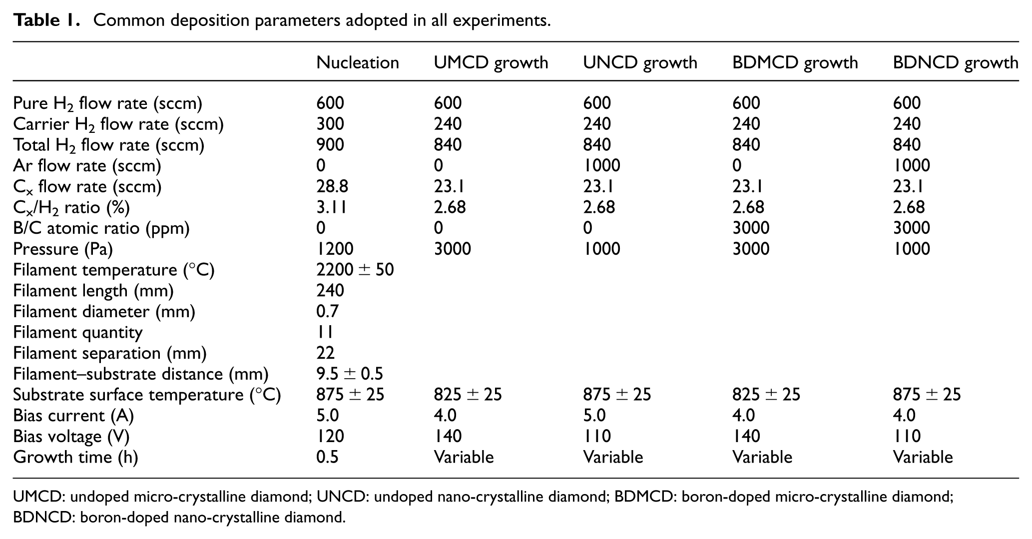
UMCD: undoped micro-crystalline diamond; UNCD: undoped nano-crystalline diamond; BDMCD: boron-doped micro-crystalline diamond; BDNCD: boron-doped nano-crystalline diamond.
Detailed experimental and sample information.
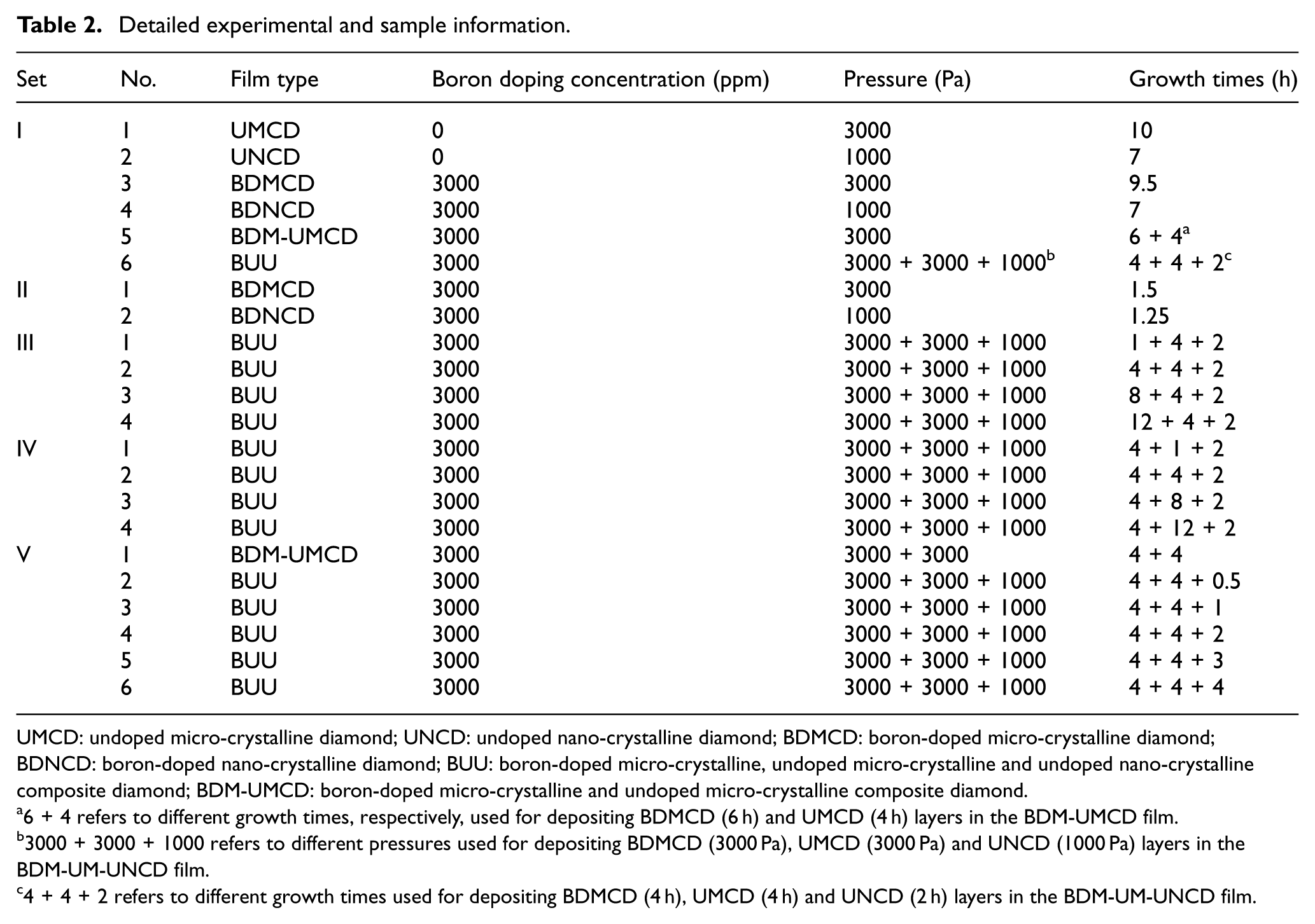
UMCD: undoped micro-crystalline diamond; UNCD: undoped nano-crystalline diamond; BDMCD: boron-doped micro-crystalline diamond; BDNCD: boron-doped nano-crystalline diamond; BUU: boron-doped micro-crystalline, undoped micro-crystalline and undoped nano-crystalline composite diamond; BDM-UMCD: boron-doped micro-crystalline and undoped micro-crystalline composite diamond.
6 + 4 refers to different growth times, respectively, used for depositing BDMCD (6 h) and UMCD (4 h) layers in the BDM-UMCD film.
3000 + 3000 + 1000 refers to different pressures used for depositing BDMCD (3000 Pa), UMCD (3000 Pa) and UNCD (1000 Pa) layers in the BDM-UM-UNCD film.
4 + 4 + 2 refers to different growth times used for depositing BDMCD (4 h), UMCD (4 h) and UNCD (2 h) layers in the BDM-UM-UNCD film.
The growth mechanism of the BDM-UM-UNCD film is illustrated in Figure 1, showing five typical stages, including the first nucleation stage (for the BDMCD layer), the BDMCD growth stage, the second nucleation stage (for the UMCD layer), the UMCD growth stage and the UNCD growth stage. During the first nucleation stage, diamond nuclei can be formed based on the micro defects or seedings on the substrate surface, indicating the effects of the pretreatment method. Detailed reasons why the following deposition process is designed by this way will be discussed later.
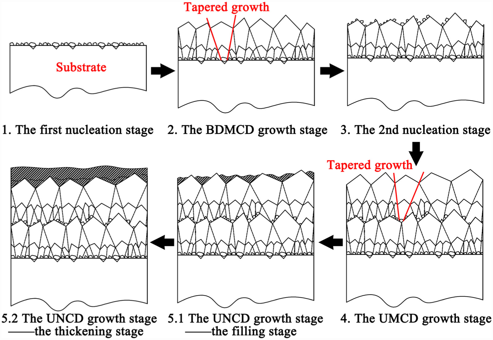
The growth mechanism of the BDM-UM-UNCD film.
Characterizations
The field emission scanning electron microscopy (FESEM; Zeiss ULTRA55) is adopted to observe both surface and cross-sectional morphologies of diamond-coated samples in order to approximately estimate grain sizes and thicknesses of as-deposited diamond films. Under some circumstances, it is difficult to distinguish the film by the FESEM, especially for composite diamond films, the boundaries between different layers are mostly vague, and it is not convenient to, respectively, observe the thickness of each layer because the observation of the cross-sectional morphology requires cutting the sample. Therefore, the thickness of as-deposited diamond film is estimated by the weighting increment during the deposition process measured by a precision balance with ±0.01 mg accuracy, and the thickness of as-deposited diamond layer is also estimated by the weighting increment divided by its area and density.
The surface roughness of the diamond film is obtained by the surface profilometer (Dektak 6M). The Ra and Rz values of as-deposited diamond film are determined by averaging five values obtained by scanning the profile curves at different positions of film surfaces, using a scanning length of 2.0 mm.
The polishability of as-grown diamond film is tested adopting a plane grinding polisher with a diamond grinding wheel and characterized by the time required for mechanically polishing the diamond film from the initial surface roughness to a definite Ra value of 50 nm under totally the same condition (the normal load = 20 N, revolving speed of the wheel = 1400 r/min, revolving speed of the sample = 10 r/min).
The surface nano hardness of the diamond-coated sample is measured by the in situ nanomechanical test system (Hysitron TI950 TriboIndenter), using a maximum load of 25 mN. The surface nano hardness is calculated on the basis of the indentation depth–load curve obtained by the nanoindentation test, using the following formulae 28
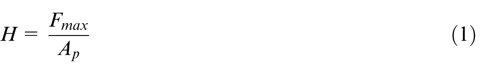
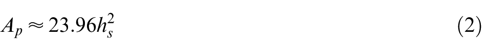
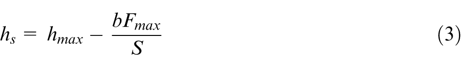
Herein, H is the calculated hardness, Fmax the maximum load, Ap the projected area of the contact between the indenter and the sample, S the slope of the initial period of the unloading curve, hs the indentation depth of the contact between the indenter and the sample, hmax the maximum indentation depth and β the geometrical parameter of the indenter. The standard Berkovich indenter is used in this study, the geometrical parameter of which is defined as 0.7268. Four different indentation points are selected for determining the average surface nano hardness of each sample.
The Raman spectroscopy (XploRA, Horiba Jobin Yvon), using a semiconductor laser with an excitation wavelength of 532 nm, is adopted to investigate the ingredient and residual stress of the diamond film. The X-ray diffraction (XRD; D8 ADVANCE) is adopted to detect chemical bonds in the diamond film.
The Rockwell hardness tester (Beijing Shidai, HR-150A) is employed to conduct the indentation test under a definite load of 980 N, and both the adhesion and the fracture strength of the diamond film are evaluated by the indentation morphology, mainly the length of the crack propagation (or the diameter of the film removal area), adopting the following formulae 29
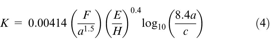
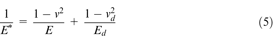
where K is the calculated fracture strength of as-deposited diamond film, F the static load used on the Rockwell hardness tester, a the semi-length or the radius of the Rockwell hardness indenter, c the length of the crack propagation, E the elastic modulus of the sample calculated from the nanoindentation test,
Results and discussion
Comparisons between different diamond films
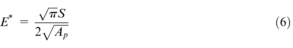
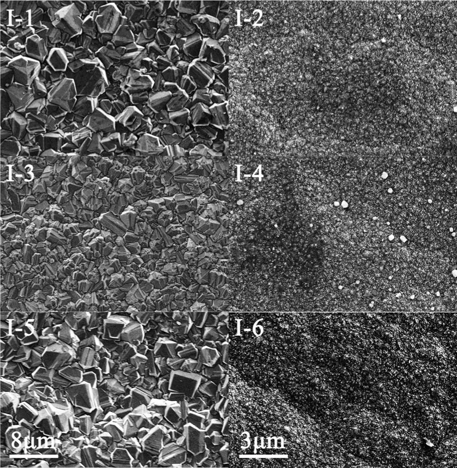
Different diamond films of similar thicknesses are first deposited on pretreated WC–6 wt% Co substrates, including the UMCD, UNCD, BDMCD, BDNCD, BDM-UMCD and BDM-UM-UNCD films, respectively, corresponding to Set I-Nos 1–6 in Table 2. The surface morphologies of as-deposited diamond films are shown in Figure 2, indicating that the UMCD and BDM-UMCD films both present continuous surfaces composed of well-defined micro-sized diamond grains, while there are a little more defects on the continuous surface of the BDMCD film composed of slightly refined micro-sized diamond grains, and other three films all have nano-sized diamond grains ∼50–200 nm in diameter which form much smoother surfaces. The surface roughness Ra and Rz values of as-deposited diamond films are all plotted in Figure 3(a). Approximately, statistical grain sizes of different diamond films are also involved in Figure 3(a). It is proved that the comparisons on the surface roughness values of different films are well consistent with the comparisons on their visible surface morphologies, which have a close relationship with their grain sizes. Specifically, the seemingly smooth surface composed of the nano-sized diamond grains shows a lower surface roughness. Nevertheless, the slight refinement of the diamond grains in the BDMCD film has no obvious effect on its surface roughness, the Ra value of which is about 304.26 nm and very close to that of the UMCD film (314.67 nm). There are also no obvious differences between surface roughness values of UNCD, BDNCD and BDM-UM-UNCD films, Ra values of which are all in the range of 95–125 nm.
Surface morphologies of different types of diamond films in Set I.
(a) Surface roughness Ra and Rz values, grain sizes and (b) polishability and nano hardness of different types of diamond films in Set I.
Figure 3(b) depicts the polishability and surface nano hardness of different diamond films. It is accessible that the polishability defined in this article, determined by averaging four polishing times conducted on a certain sample, is dependent on the initial surface roughness and the surface hardness. The reduction in the initial surface roughness can directly reduce the polishing allowance (i.e. the required decline of the surface roughness), and the surface hardness reduction can enhance the polishing efficiency. As a result, nano-sized diamond films all present much better polishability than micro-sized diamond films, manifesting as much shorter required polishing time. Besides, the polishability of the BDMCD film is also a little better than that of the UMCD one, mainly because of the slightly reduced surface hardness. Reasons for different surface nano hardness values will be explained later.
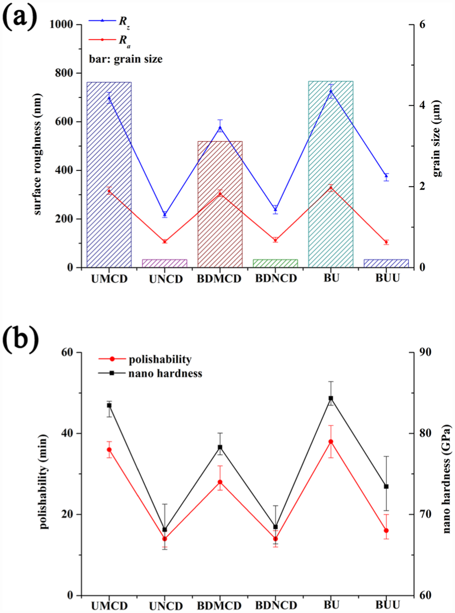
Cross-sectional morphologies of as-deposited diamond films are shown in Figure 4, first proving that in Set I, different diamond films of similar thicknesses (16–20 µm) have indeed synthesized by controlling growth times. It is also found that the boron doping technology can slightly increase the growth rate of the diamond film, and the growth of the NCD film is much faster than that of the micro-crystalline diamond (MCD) film under either the undoped or boron-doped conditions because more radicals move to substrate surfaces and the substrate temperature apparently increases at a relatively lower pressure of 1000 Pa. Moreover, obvious tapered growth structures can be noticed from cross-sectional morphologies of UMCD, BDMCD and BDM-UMCD films, but for both UNCD and BDNCD films, there are dense accumulated structures observed from cross-sectional morphologies, while for the BDM-UM-UNCD film, the cross-sectional growth form of diamond grains gradually transfers from the tapered structure to the dense structure and there is blurring boundary between them. Comparatively speaking, boundaries between UMCD layers and BDMCD layers are invisible for both of the composite films. It is significant that the tapered growth structure will cause the competitive growth of micro-sized diamond grains, and the grains appearing on the surface are much larger than the initial diamond nuclei, just as shown in Figure 1. For the sake of estimating the film/layer thickness by the weighting method as accurately as possible in following researches, based on statistic data obtained from amounts of samples covered by some monolayer diamond film (Set I-Nos 1–4), including film thicknesses observed by FESEM and corresponding weight increments measured by the precision balance, the densities of UMCD, UNCD, BDMCD and BDNCD films are, respectively, calculated as 3.317, 3.260, 3.337 and 3.228 g/cm3, almost the same. Consequently, thicknesses of different layers in the BDM-UMCD film are, respectively, calculated as 13.78 µm (BDMCD layer) and 7.15 µm (UMCD layer), and those in the BDM-UM-UNCD film are 8.95 µm (BDMCD layer), 8.28 µm (UMCD layer) and 3.51 µm (UNCD layer). Herein, each thickness is also obtained by averaging weight increments of four different samples.
Cross-sectional morphologies of different types of diamond films in Set I.
The Raman spectra are all presented in Figure 5. It is well known that in the Raman spectrum of the diamond film, the peak close to 1332.4 cm−1 denotes the typical peak of the sp3 diamond phase, and the shift of this peak relative to 1332.4 cm−1 (the position of the diamond peak for the natural diamond without residual stress) indicates the existence of the residual stress in the film. The estimation of the residual stress value in the diamond film based on the Raman spectrum can refer to the research of Ralchenko et al. 30 A sharp sp3 diamond peak exists, centered at 1335.9 cm−1 in the Raman spectrum of the UMCD film, along with few minor non-diamond peaks, indicating very high diamond purity and a compressive residual stress of 1.9845 GPa. The total residual stress in the diamond film includes the thermal residual stress and the growth residual stress. The former is caused by the thermal expansion coefficient difference between the diamond and the substrate during the cooling down process of the diamond-coated sample from the substrate temperature to the room temperature after the deposition duration, which is primarily compressive stress for the WC–6 wt% Co substrate, while the latter arises from either the non-diamond phase or the defect in the film and at boundaries, like microtwins, dislocations, impurities, among others. 31 For instance, due to the fact that the specific volume of the graphite is 1.5 times larger than that of the diamond, the graphite carbon mingled in the diamond film is responsible for the augment of the compressive residual stress. 32 Besides, the existence of oxygen atoms, which come from the acetone, can also induce certain compressive stress because the covalent radius of the oxygen atom (0.066 nm) is smaller than that of the carbon (0.077 nm). 33 Consequently, the UMCD film deposited on the WC–6 wt% Co substrate presents obvious compressive residual stress as high as 1.9845 GPa.
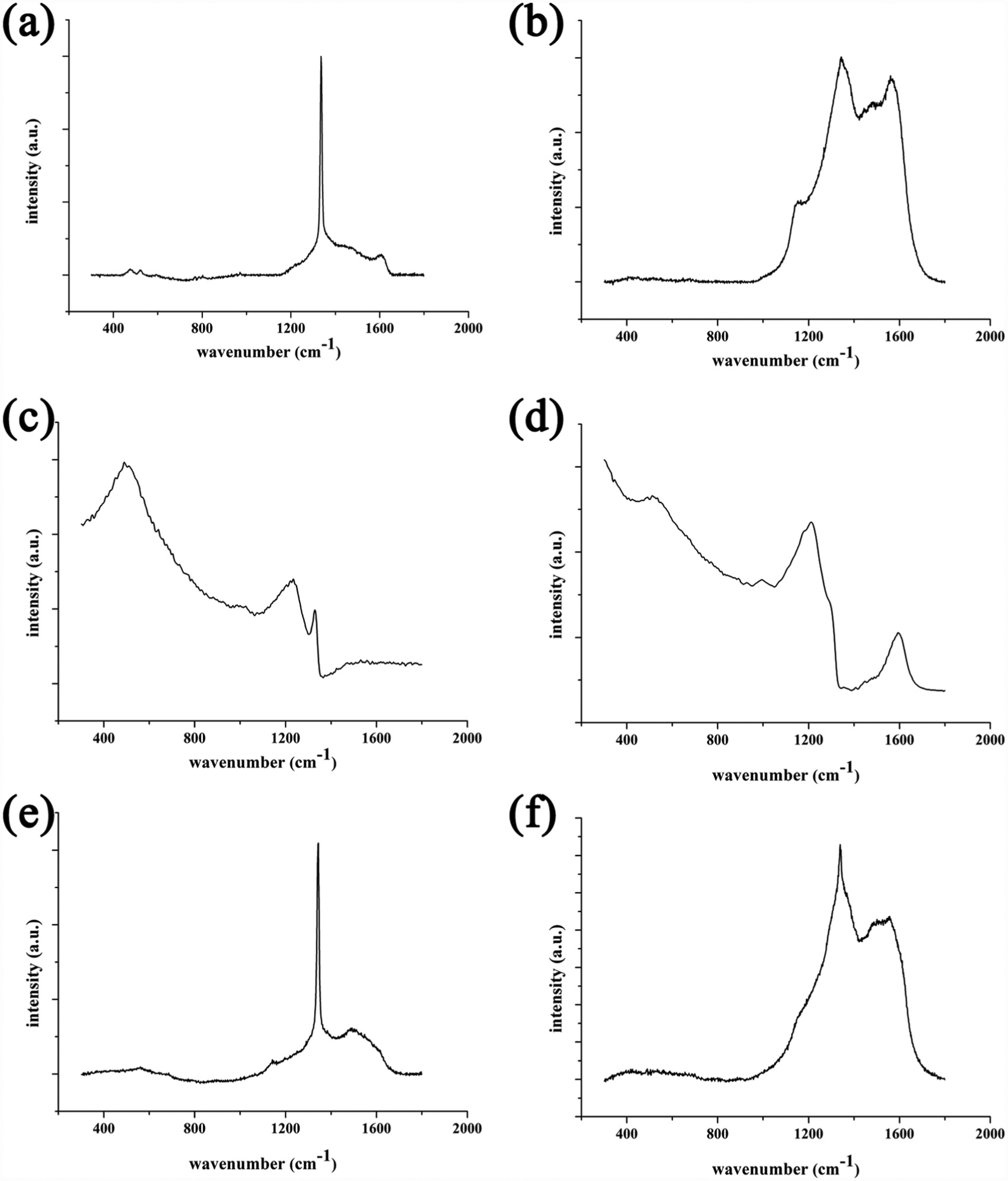
Raman spectra of (a) UMCD, (b) UNCD, (c) BDMCD, (d) BDNCD, (e) BDM-UMCD and (f) BDM-UM-UNCD films in Set I.
Observed from the Raman spectrum of the UNCD film, the sp3 diamond peak centered at 1337.6 cm−1 is significantly broad, indicating the existence of nano-sized diamond grains and much lower diamond purity as compared with the UMCD film. The pronounced Raman scattering intensity in the region of 1400–1600 cm−1 also suggests that the grain size of the UNCD film has decreased to nanometer scale, 27 and the graphitic G band (around 1580 cm−1) and D band (around 1350 cm−1) are both visible. 34 Two additional bands around 1150 and 1480 cm−1 are both assigned to transpolyacetylene. 35 As calculated from the shift of the sp3 diamond peak, the compressive residual stress in the UNCD film reaches as high as 2.9484 GPa, which should be attributed to much more non-diamond purities accumulated in numerous boundaries of such films. It is also supposed that the increment of impurities in the diamond film can cause remarkable reduction in the hardness, that is why the UNCD film shows much lower surface nano hardness value (68.11 GPa) as compared with the UMCD film (83.46 GPa), as illustrated in Figure 3(b).
As for the BDMCD and BDNCD films, relatively broad sp3 diamond peaks with low intensities, respectively, centered at 1333.3 and 1334.7 cm−1 are overlaid by broad features with a maximum around 1250 cm−1, which is associated with the actual boron incorporation in the lattice, so is the broad band around 500 cm−1. 36 It should be noted that the compressive residual stress values of both BDMCD (0.5103 GPa) and BDNCD (1.3041 GPa) films are much lower than that of the UMCD one, let alone that of the UNCD one, mainly because the covalent radius of the boron atom (0.085 nm) is larger than that of the carbon atom, and thus induces a certain tensile residual stress. 33 Comparatively speaking, the compressive residual stress of the BDNCD film is higher than that of the BDMCD film. Besides, boron doping technology can also reduce the diamond purity, manifesting as the slight broaden of the diamond peak in the Raman spectrum of the BDMCD film, as well as the obvious broaden of the diamond peak and the appearance of the pronounced Raman scattering intensity in the region of 1400–1600 cm−1 in the Raman spectrum of the BDNCD film. Without regard to the boron-related peaks, the BDMCD film shows a Raman shape similar to the UMCD one, and the BDNCD film shows a Raman shape similar to the UNCD one. The more non-diamond phases, together with the more surface defects can illuminate why the surface nano hardness value of the BDMCD film (78.32 GPa) is a little lower than that of the UMCD one and that of the BDNCD film (68.45 GPa) is even lower, as mentioned in Figure 3(b).
As for the BDM-UMCD film, the Raman spectrum only represents the features similar to the single-layer UMCD film, with a sharp sp3 diamond peak centered at 1334.1 cm−1, indicating that boron atoms doped in the underlying layer have no obvious effect on the diamond purity of the surface layer, hence its surface nano hardness value (84.36 GPa) is as high as that of the UMCD film. But the total compressive residual stress of the BDM-UMCD film significantly reduces to 0.9639 GPa, which can be ascribed to the relieving effect of the underlying UMCD layer. Furthermore, a feature similar to the Raman spectrum of the UNCD film is exhibited in the Raman spectrum of the BDM-UM-UNCD film, with a relatively narrow sp3 diamond peak centered at 1335.9 cm−1. The narrowing of the sp3 diamond peak as compared with the UNCD film might be attributed to the effect of the UMCD layer beneath the thin surface UNCD layer, which is able to be detected in the Raman observation. Also mainly owing to the relieving effect of the underlying UMCD film, the compressive residual stress of such films (1.9845 GPa) is much lower than that of the single-layer UNCD film.
Interestingly, as shown in Figure 3(b), the surface hardness of the BDM-UM-UNCD film is unexpectedly much higher than those of single-layer UNCD and BDNCD films, although they have almost the same ingredients and surface properties. It is believed that for the coated sample, if the indentation depth exceeds 1/10 of the film thickness, the substrate will contribute to the measured nano hardness. As shown in Figure 1, the growth stage of the UNCD layer is divided into two stages: the filling stage and the thickening stage, meaning that numerous UNCD grains will first fill valleys between UMCD grains and then cover the whole UMCD surface, in consequence, although the thickness of the UNCD layer is measured as 3.51 µm by the weighting method, its actual thickness is only 2–3 µm, but the indentation depth is as high as 250 nm, so the middle UMCD layer contributes much to the measured surface nano hardness of such composite films. In applications of diamond-coated components suffering severe wear under macroscopical conditions, the reinforcement of the surface hardness might improve the wear resistance of the composite film to some extent. More importantly, after the initial wear or polishing removal of the surface UNCD layer, the residual film can present not only favorable surface roughness caused by the filling of UNCD grains in valleys between UMCD grains but also excellent wear resistance provided by the ultra-hard middle UMCD layer.
The adhesion of the diamond film is of paramount importance in its applications because the delamination and peeling of the film are the main failure mode of the film. In this article, the indentation morphology of the diamond film under a definite load of 980 N is obtained by the Rockwell hardness tester and observed by the FESEM to evaluate its adhesion and fracture strength, as stated in Figure 6. As a matter of fact, in this study, the adhesion of the diamond film is qualitatively estimated by the length of the crack propagation (or the diameter of the film removal area), and the fracture strength is also mainly influenced by the length of the crack propagation, so the adhesion and fracture strength present similar trends. Here, each value of the length of the crack propagation is also obtained by averaging the lengths of the crack propagation on four different samples, but the fracture strength value is calculated using the average hardness, elastic modulus and the length of the crack propagation.
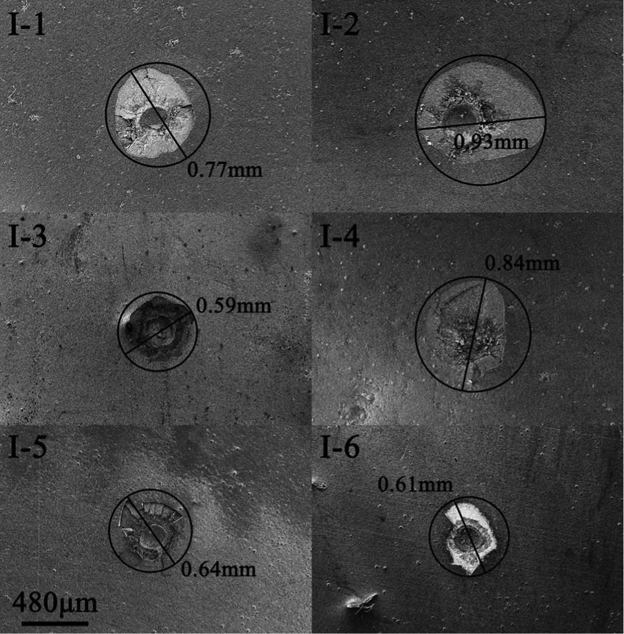
Indentation morphologies of different types of diamond films in Set I, obtained by the Rockwell hardness tester.
The length of the crack propagation and the fracture strength of the UMCD film are, respectively, 0.77 mm and 1.048 MPa m0.5. For the UNCD film, the film removal extends to a 0.93-mm-wide area, and the fracture strength value accordingly decreases to 0.69 MPa m0.5, which can be attributed to the more impurities at the interface, the increase in the residual stress and the poor mechanical cohesion between nano-sized diamond grains and the substrate. By contrast, the length of the crack propagation of the BDMCD film significantly decreases to 0.59 mm, and its fracture strength value accordingly increases to 1.337 MPa m0.5. The relieving of the residual stress is recognized as one of the prominent reasons why the boron doping technology can enhance the adhesion of the diamond film, and another reason should be the formation of B–Co compounds close to the film–substrate interface, which can reduce the graphitization effect of the Co element and prohibit the deeper Co from moving to the interface. B–Co bonds can be indeed detected at the positions close to interfaces of both BDMCD and BDNCD films by the XRD, for example, as plotted in Figure 7, the peaks close to 44° indicate the existence of CoWB. The detective depth of the XRD is limited, so all detections are conducted on samples coated with 3-µm-thickness films (Set II). Unfortunately, the BDNCD film, in which the B–Co bond also exists and the compressive residual stress is even less than that in the UMCD film, still shows a film removal area (Φ = 0.84 mm) larger than the UMCD film, probably because the poor mechanical cohesion has considerable influence on its adhesion, and the reduction in the compressive residual stress caused by the boron atom doping cannot substantially offset the severe influence of abundant impurities on its adhesion. As a result, in the design of composite diamond films, the BDMCD film is finally selected as the under layer, which is proved to be effective on the issue of improving the adhesion and the fracture strength of composite diamond films, consistent with the previous research. 37 Concretely, the length of the crack propagation and the fracture strength value of the BDM-UMCD film are, respectively, 0.64 mm and 1.312 MPa m0.5, and those of the BDM-UM-UNCD film are 0.61 mm and 1.27 MPa m0.5, both close to those of the single-layer BDMCD film.
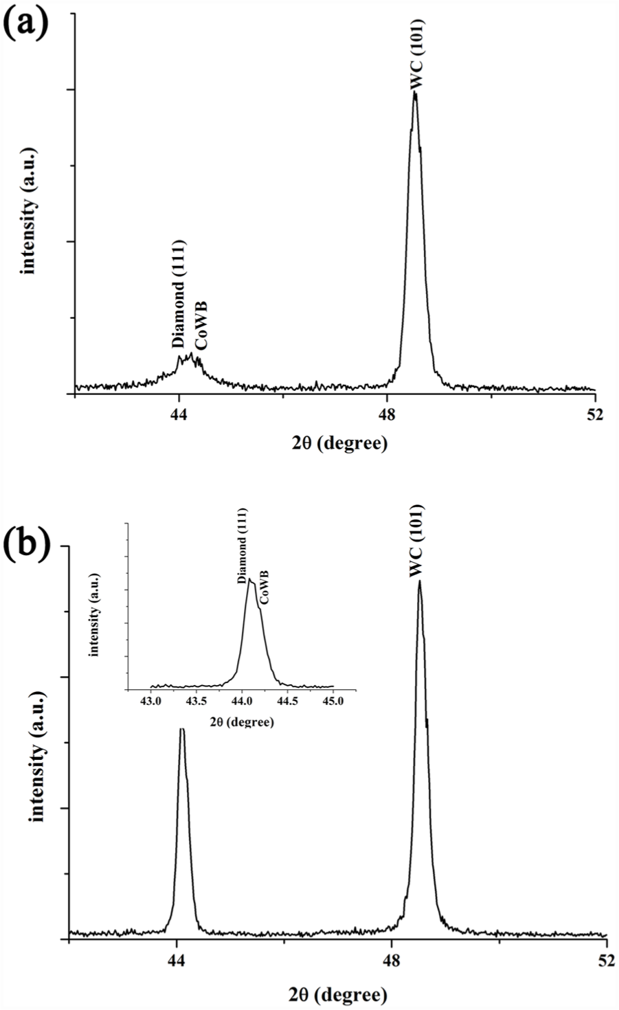
XRD spectra of 3-µm thickness: (a) BDMCD and (b) BDNCD films.
Optimization of growth times for BDMCD and UMCD layers
It has been proved in our previous study that the thickness of the BDMCD film or the UMCD film has significant influences on the grain size, residual stress, fracture strength and adhesion. 14 Considered from similar aspects, growth times for UMCD and BDMCD layers in the BDM-UM-UNCD film, which are directly related to their thicknesses, are optimized in the present investigation, using the parameters listed in Table 2 (Sets III and IV). Detailed relationships between characterization results and growth times for the underlying BDMCD layer and the middle UMCD layer are, respectively, illustrated in Figures 8–10.
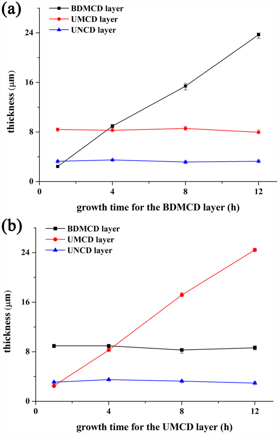
Detailed relationships between the film/layer thickness and growth times for (a) BDMCD and (b) UMCD layers in the BDM-UM-UNCD film.
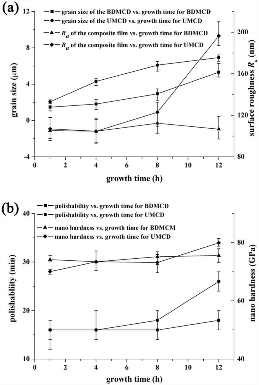
Detailed relationships between growth times for BDMCD/UMCD layers in the BDM-UM-UNCD film and (a) grain sizes of corresponding layers and the Ra value of the BDM-UM-UNCD film, as well as (b) the polishability and the nano hardness of the BDM-UM-UNCD film.
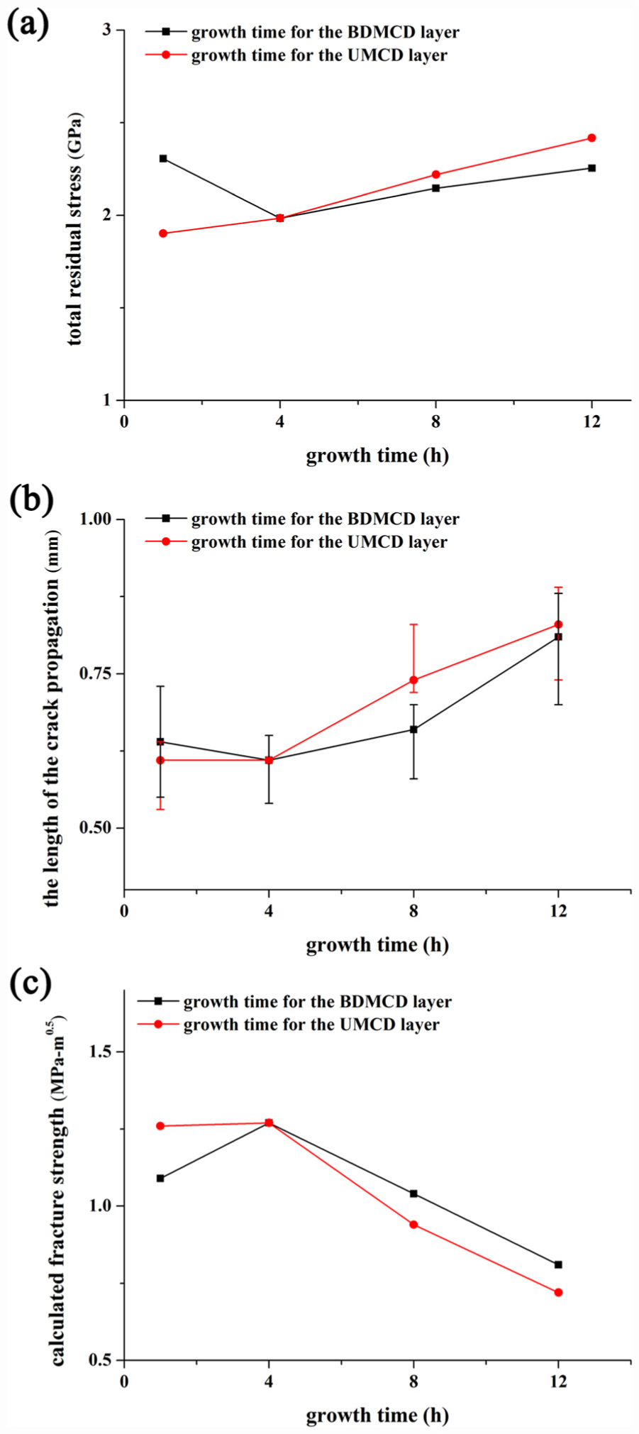
Detailed relationships between (a) the residual stress in the BDM-UM-UNCD film, (b) the length of the crack propagation on the surface of the BDM-UM-UNCD film under the Rockwell indentation test, together with (c) the calculated fracture strength value of the BDM-UM-UNCD film and growth times for BDMCD and UMCD layers in the BDM-UM-UNCD film.
In the present investigation, thicknesses of all diamond layers are obtained by the weighting method. The thickness of the BDMCD layer is proportional to its growth time, so is the thickness of the UMCD layer, but the increment of the growth time for a certain layer has no obvious influences on thicknesses of other layers, as shown in Figure 8. However, the thickness of the surface UNCD layer, which is evaluated directly by the FESEM but not the weighting method, has actually changed by increasing the growth time for the middle UMCD layer, especially when such time reaches 12 h, which is demonstrated by Figure 11(a), typifying the surface not totally covered by UNCD grains. This phenomenon should be attributed to the growth mechanism of such composite diamond films, as demonstrated in Figure 1. It is easy to understand that grain sizes of the BDMCD and UMCD layers will become larger with increasing their growth times, as proved in Figure 9(a), because of the tapered growth of the micro-sized diamond grains (as depicted in Figures 1 and 4). The change in the surface grain size of the UMCD layer will cause deeper valleys between UMCD grains on the surface of the BDM-UMCD layer, and thus more UNCD grains are required to fill them at the filling stage. As a result, the weighted thickness of the surface UNCD layer represents filled grains more than the covered layer. For the same reason, the surface roughness of the composite film also slightly increases when the growth time for the middle UMCD layer reaches 12 h, also as demonstrated in Figure 9(a). Furthermore, under such conditions, the property of the UMCD layer can contribute much more to the surface UNCD layer, for which the nano hardness value of the composite diamond film increases, and thus the required polishing time is accordingly elongated, as shown in Figure 9(b). By contrary, it should be noted that when the growth time for the middle UMCD layer decreases from 4 to 1 h, the nano hardness value of the composite diamond film also slightly reduces from 73.44 to 70.09 GPa because the thin UMCD layer cannot provide sufficient reinforcement effects for the surface hardness of the composite diamond film, and under such conditions, the surface hardness value may be even affected by the BDMCD layer. As for the growth time for the BDMCD layer, the grain size of the BDMCD layer will also increase with the growth time, but such change cannot cause obvious variations in the surface roughness, polishability and nano hardness of the composite diamond film due to the isolation of the middle UMCD layer, also as presented in Figure 9.
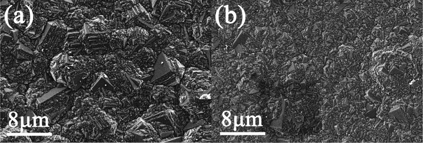
Surface morphologies of BDM-UM-UNCD films not totally covered by surface UNCD layers: (a) Set IV-No. 4 and (b) Set V-No. 2.
There is no doubt that the increment of the growth times for either the BDMCD or the UMCD layer will induce the increment of the thickness of the composite diamond film, for which under the identical deposition condition, the total residual stress in the whole composite film will increase when either of the growth time increases from 4 to 12 h, as demonstrated in Figure 10. Set IV-No. 4 still presents a typical Raman spectrum shape similar to Set I-No. 6, as shown in Figure 12, although its surface has not been completely covered by the UNCD layer, because the nano-sized UNCD grains filled in valleys between UMCD grains, which contain abundant non-diamond phases at boundaries, can sufficiently contribute to the Raman spectrum. For the BDM-UM-UNCD film, it is supposed that both the film–substrate adhesion and the fracture strength have close relationships to the residual stress in the film, so the length of the crack propagation also increases with either of the growth time, in the range of 4–12 h, and the calculated fracture strength decreases. It should be emphasized that the increasing in the growth time for the BDMCD layer has less adverse effect on the residual stress, crack propagation length and fracture strength then that for the UMCD one. Specifically, increases in the residual stress per thickness increment for the BDMCD and UMCD films are, respectively, 0.0167 and 0.0293 GPa/µm, and increases in the crack propagation length are 0.0124 and 0.0149 mm/µm, and decreases in the fracture strength are 0.0285 and 0.0373 MPa m0.5/µm. On the contrary, when the growth time for the BDMCD layer decreases from 4 to 1 h, the total residual stress and the length of the crack propagation also increase, and the fracture strength accordingly decreases, indicating that the thin BDMCD layer cannot effectively relieve the residual stress in the composite film and enhance its adhesion.
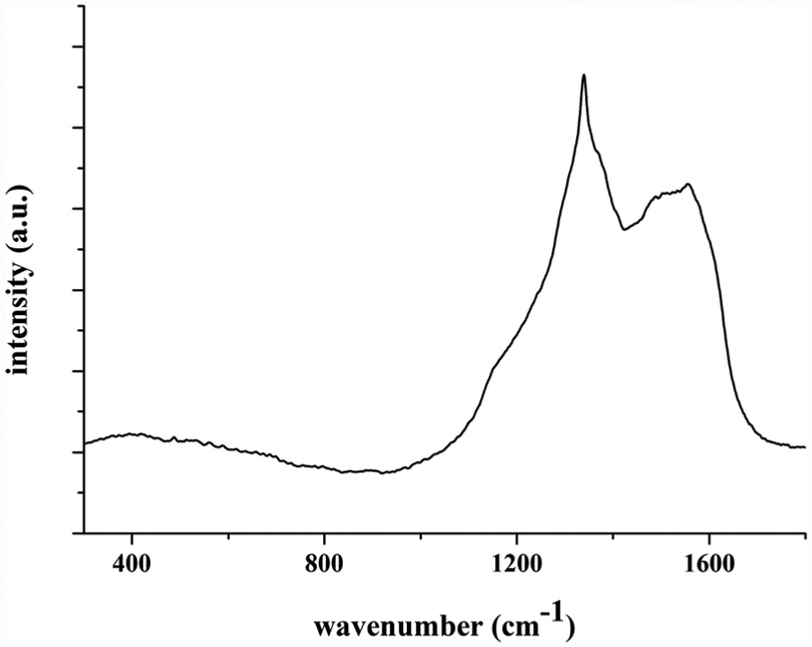
Raman spectrum of a typical BDM-UM-UNCD film whose surface has not been completely covered by the UNCD layer (the Set IV-No. 4 sample).
In summary, for the sake of guaranteeing the surface hardness, adhesion and the fracture strength of the BDM-UM-UNCD film, growth times for UMCD and BDMCD layers should be moderate, which are both determined as 4 h in this study.
Optimization of the growth time for the BDNCD layer
As described above, if the growth time for the middle UMCD layer increases to 12 h and its grain size increases to 9 µm, the surface UNCD layer growing for only 2 h cannot totally cover the micro-sized UMCD grains. The similar phenomenon also exists when reducing the growth time for the BDNCD layer to 0.5 h (Set V-No. 2), as shown in Figure 11(b). In consequence, the surface roughness Ra value, polishability and the nano hardness of the BDM-UM-UNCD film are all intimately associated with the growth time for the BDNCD layer, as demonstrated in Figure 13(a). It is evident that in the whole scope of the growth time for the BDNCD layer (0–4 h), the nano hardness value of the BDM-UM-UNCD film monotonically decreases with increasing such growth time because either the complementally filling of the UNCD grains in the valleys between the UMCD grains or the covering of the thicker UNCD layer on the UMCD layer can weaken the reinforcement effect of the middle UMCD layer on the surface hardness of the composite film. As mentioned above, the growth of the surface UNCD layer is divided into two stages: the filling stage (0–2 h) and the thickening stage (2–4 h). The surface roughness of the composite diamond film distinctly decreases at the filling stage, therefore its polishability is significantly enhanced, manifesting as a sustained downward trend in the required polishing time, indicating that the coverage of the nano-sized UNCD grains on the micro-sized UMCD grains play important roles on both the initial surface roughness and the polishability of the composite diamond film. Nevertheless, at the thickening stage, the continued thickening of the surface layer barely affects either the initial surface roughness or the polishability of the composite film because the grain size of the surface UNCD layer remains around 50–100 nm, and there is no obvious differences between the hardness and other intrinsic properties of the UNCD layers of different thicknesses.
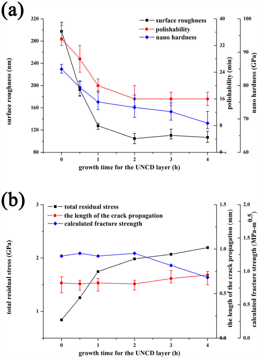
Detailed relationships between the growth time for the surface PNCD layer and characterization results: (a) the Ra value, polishability and the nano hardness of the BDM-UM-UNCD film and (b) the residual stress in the BDM-UM-UNCD film, the length of the crack propagation on the surface of the BDM-UM-UNCD film under the Rockwell indentation test and the calculated fracture strength value.
Variations in the total residual stress in the composite diamond film, the length of the crack propagation under the Rockwell indentation and the fracture strength of the composite film with the growth time for the UNCD film are all illustrated in Figure 13(b), indicating that the total residual stress significantly increases with this growth time, especially at the filling stage, with the filling and covering of UNCD grains on the UMCD grains, the total residual stress sharply increases from 0.8417 to 1.9845 GPa, due to the rapid and mass formation of grain boundaries and non-diamond impurities. However, there are no obvious distinctions on the length of the crack propagation and the calculated fracture strength value between different samples obtained at the filling stage (Set V-Nos 1–4), probably because the increment of the total residual stress caused by the local impurities barely influences the macroscopical structural property of the composite film. Only in the thickening stage, the continuous increment of the total residual stress caused by the substantial thickening of the surface UNCD layer, that is, the substantial thickening of the whole composite diamond film, will contribute much to the propagation of the crack and deteriorate the fracture strength of the composite diamond film.
In summary, mainly for guaranteeing the initial surface roughness, the polishability, the coverage of nano-sized UNCD grains on micro-sized UMCD grains and the surface hardness of the BDM-UM-UNCD film, the growth time for the UNCD layer should also be moderate, which is determined as 2 h in this study.
Finally, it must be mentioned that thicker composite diamond films are probably required in some applications. Comparatively speaking, the thickness increment of the BDMCD layer has the least adverse influences on properties of the composite film. Consequently, under such conditions, the growth time for the BDMCD layer can be elongated as required, but growth times for UMCD and UNCD layers had better be fixed.
Conclusion
A novel composite diamond film named BDM-UM-UNCD film is designed and deposited on the pretreated WC–6 wt% Co substrate. Following conclusions are drawn:
The underlying BDMCD layer can effectively enhance the film–substrate adhesion due to the relieving of the residual stress, the nice mechanical cohesion between the micro-sized diamond grains and the substrate, as well as the formation of the B–Co bonds.
The surface UNCD layer presents relatively lower initial surface roughness and nano hardness, hence the composite film is much easier to be mechanically polished to the required surface smoothness.
The middle UMCD layer can reinforce the surface hardness of the composite film. Especially, after the initial wear or polishing removal of the surface layer, the residual diamond film may present excellent wear resistance due to the effect of the ultra-hard middle layer.
The thickness increments of the BDMCD layer or UMCD layer will both deteriorate the adhesion and the fracture strength of the composite film. Besides, the BDMCD layer with insufficient thickness cannot provide enough improving on the film–substrate adhesion, while the excessive thickness reduction in the UMCD layer will weaken its reinforcement effect on the surface hardness of the composite film. Therefore, growth times for UMCD and BDMCD layers should be moderate, which are both determined as 4 h in this study.
The growth stage of the UNCD layer can be divided into the filling stage and thickening stage. Too short growth time for such layers cannot guarantee the complete coverage of nano-sized UNCD grains on micro-sized UMCD grains, inducing higher initial surface roughness and surface hardness, and thus makes polishing much more difficult. The excessive thickening of the surface layer will either deteriorate the adhesion or suppress the reinforcement effect of the middle layer on the surface hardness. In consequence, the growth time for the UNCD layer should also be moderate, which is determined as 2 h in this study.
Footnotes
Appendix 1
Declaration of conflicting interests
The author(s) declared no potential conflicts of interest with respect to the research, authorship and/or publication of this article.
Funding
The author(s) disclosed receipt of the following financial support for the research, authorship, and/or publication of this article: This research was supported by the National Natural Science Foundation of China (Nos 51275302 and 51375011) and China Postdoctoral Science Foundation (No. 15Z102060056).