
Abstract
This study introduces an approach for converting the current from a sensor into controllable voltage. To this end, a switched-capacitor structure was integrated to provide efficient current-to-voltage conversion. The generated voltage was further regulated by an operational amplifier current source, enhancing stability and precision. An n-type metal oxide semiconductor field-effect transistor structure under an H-bridge was integrated into the system to achieve fine-tuned control over current stimulation. This component contributed to voltage regulation and enabled bi-directional control of current flow, offering versatility in adjusting current amplitudes using working and counter electrodes. This dynamic control mechanism was pivotal for effectively controlling the intensity of current stimulation. We applied Verilog-A modeling to simulate the optical characteristics of Si nanowires. The proposed system efficiently converted sensor-derived current into voltage using a switched-capacitor structure. Simultaneously, the precision was enhanced via operational amplifier regulation and n-type metal-oxide-semiconductor field-effect transistor-based H-bridge control. The simulation showed a current stimulus amplitude ranging from 2 to 13 μA for a variable photocurrent of Si nanowires (Rex: 10 kΩ, pulse: 100 Hz, 1 ms). The ability to finely control current stimulation intensity holds promise for diverse applications requiring accurate and adjustable current manipulation. This study contributes to the growing field of sensor technology by offering a unique perspective on the integration of nanostructures and electronic components for an enhanced control and functionality.
Keywords
Introduction
Retinal prostheses are a promising technology for restoring vision in individuals who have lost their eyesight because of retinal degenerative diseases. These devices are categorized on the basis of the location of electrode insertion and method of receiving visual information from the front.1,2 The position of the electrode insertion varies with the target cell for stimulation; thus, several types of retinal prostheses can be obtained. Various methods, including the modulation of electrical pulses to control the delivery of charge to the retinal tissue, have been employed in these prostheses. Techniques such as pulse amplitude modulation (PAM), pulse width modulation, and pulse frequency modulation are commonly used in medical applications to precisely control the amount of charge delivered for electrical stimulation in retinal prostheses. 3 Intentional current injection is a common practice in such medical applications. In retinal prosthetics, ensuring stable operation and minimizing device size are crucial. Therefore, the integration of technologies that provide reliable and compact solutions for electrical stimulation is crucial. The Argus 2 system was the first commercially available product to process visual information through a camera and apply current stimulation patterns to electrodes inserted into the eye. 4 For PRIMA system, visual information is processed using a camera and current stimulation patterns are provided by irradiating the photodiode array inserted into the eye using a short-wavelength laser. 5 For Alpha AMS, current stimulation is applied using a microphotodiode array. 6 Although each has its advantages and disadvantages, Argus 2 and PRIMA use a camera. By contrast, Alpha AMS does not use a camera, but the system is reported to be bulkier than those employed in other methods and has a problem when inserted. Therefore, we aimed to simulate whether a system such as the Alpha AMS can be implemented using the parameters of a Si nanowire photodetector, which can be implemented in a smaller size than that of a microphotodiode array. Nanowires are known for their high surface- to-volume ratio, which significantly enhances their photoresponsivity. The high surface area of nanowires allows for greater interaction with incident light, improving the efficiency of photodetection. Recent advancements in this field involve the integration of sensors for visual information, enabling the implantation of devices that receive visual input internally rather than relying on external cameras. This integration significantly enhances the capabilities of the retinal prostheses. These prosthetic devices offer users a natural and responsive visual experience by eliminating reliance on external cameras. Reliance on cameras often creates a gap between artificial and natural vision, such as the lack of eye movement when not turning one's head. Therefore, this development bridges the gap between artificial and natural vision and enables advancement toward user-friendly retinal prosthetics without the need for external devices. These advancements show significant potential for improving the quality of life of individuals with vision loss, creating possibilities for integrated and immersive visual perception that closely aligns with the natural functioning of the human eye.6,7
Circuit design
Retinal prostheses are classified on the basis of the location of electrode insertion and method used to perceive visual information. The placement of electrodes varies with the target cells used for stimulation. Some designs incorporate both electrodes and visual information reception within the eye, typically by capturing visual data from an external camera and converting them to stimulate cells. A design has been developed to enhance this approach by integrating a sensor that receives visual information directly, along with electrodes, into the eye. For this purpose, a circuit that combines Si nanowire photodetectors and biphasic stimulators has been designed. This integration aims to merge the reception of visual information with electrodes within the eye. The circuit design was developed using a TSMC 180 nm process design kit (Figure 1). 8

Overview of the proposed implantable retinal prostheses.
Design of Verilog-A for Si nanowire
For the Verilog-A model of Si nanowires, we fabricated nanowires and measured their currents. The width of the fabricated nanowires was 150 nm with a spacing of 2 μm, and measurements were taken from 250 Si nanowires.9,10 During the fabrication process, SiO2 and Si were etched following wet oxidation and deep reactive ion etching to produce Si nanowires. 11 The method of measurement involved altering the lighting conditions (specifically white light), as illustrated in Figure 2(a), and recording the resultant changes in the current flowing through the Si nanowire. This experiment confirmed the optical properties of the Si nanowires, enabling the design of a Verilog-A model for Si nanowires. A broader range was considered for the simulation to accommodate potential variations owing to differences in the number of wires or fabrication errors. A broad range was considered in the simulation. As shown in Figure 2, the resistance of the Si nanowire photodetector varied from hundreds of kilohms to 10 MΩ. Consequently, the sweep of the simulation ranged from 10 kΩ to 11 MΩ, including the modeling of the variable resistance as shown in Figure 2(b). Therefore, a capacity of 50 pF was used because the capacitance must be sufficiently large to obtain a distinguishable charging voltage when the photocurrent of the Si nanowire is increased proportionally with the amount of light.
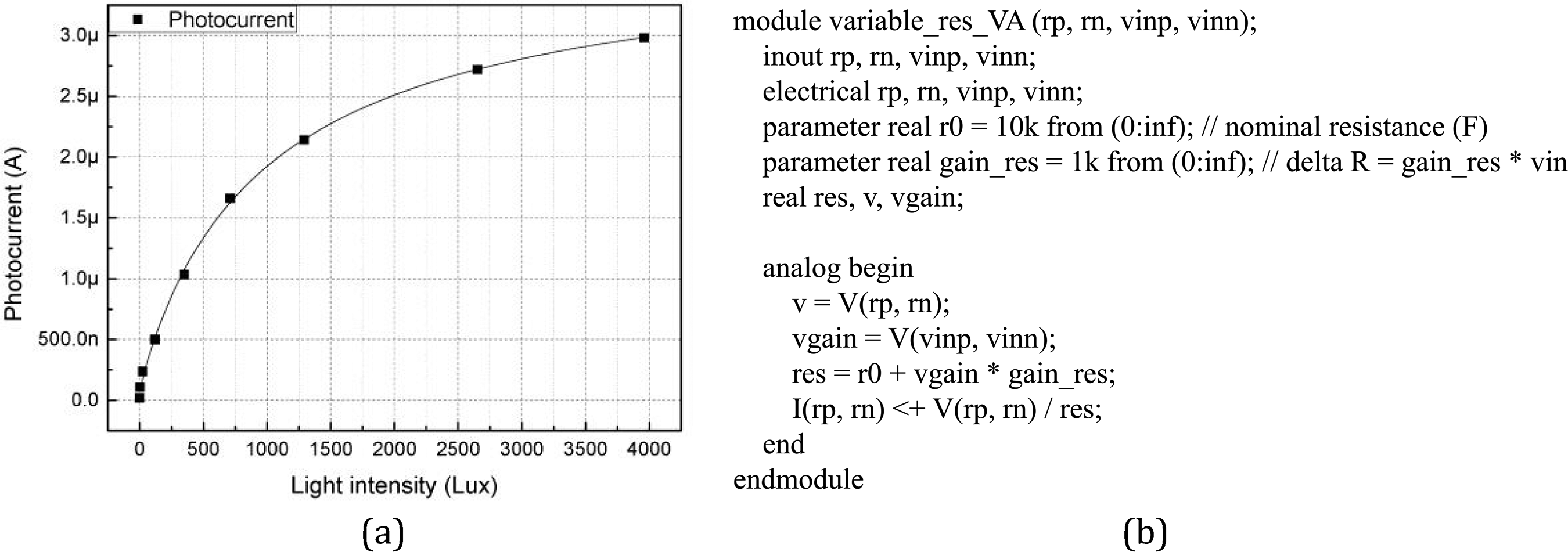
(a) Si nanowire IV characteristics 10 and (b) Si nanowire Verilog-A model.
Design of switched capacitor structure
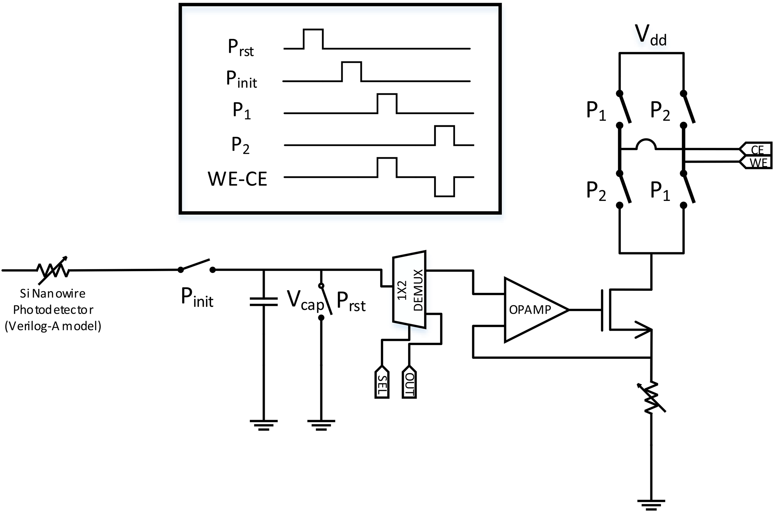
Si nanowire sensors are light-responsive current sources capable of adjusting current on the basis of light intensity. These sensors dynamically alter their current output in response to varying light conditions, rendering them highly suitable for applications requiring sensitivity to light intensity. To effectively regulate the current flowing through the working electrode (WE) and counter electrode (CE), a suitable I–V (current-to-voltage) converter was incorporated into the H-bridge configuration. To this end, we employed a switched capacitor structure. This structure was designed to convert the current, which was modulated on the basis of the light intensity detected by the Si-nanowire sensor, into a corresponding voltage. Three specific signals were employed to convert the current into voltage in the switched-capacitor structure:
Additionally, in the designed switched capacitor structure, the resistance of the silicon nanowires and the circuit capacitance function as a low-pass filter, significantly reducing noise before it affects current control in the low dropout regulator via the amplifier. Noise beyond the bandwidth of amplifier is naturally attenuated, and the parallel RC configuration of the WE and CE further filters out switching noise. Considering the millisecond-scale refractory period of the cells, our system operates without high-speed switching, reducing the occurrence of typical switching noise (Figure 3).


Schematic of switched capacitor structure.
Design of amplifier
In a previous study, a two-stage operational amplifier (OPAMP) was used to control the gate of an NMOS. 14 However, the output voltage range obtained by this approach was limited. A folded cascode structure was considered to address this issue, owing to its ability to expand the voltage swing despite a reduction in gain compared with that of the standard cascode. Consequently, a rail-to-rail folded cascode amplifier was developed to address the limitation. 15 In the sensor section, the current was converted into voltage using a switched capacitor structure, ensuring that the amplifier transformed a stable voltage supply into a variable current source at the NMOS gate. This amplifier was designed explicitly with a rail-to-rail input, enabling the utilization of the voltage input range from 0 to Vdd. 16 Additionally, the output stage was configured as a single-end output, in contrast to a conventional two-stage bulk-drive folding cascode amplifier, to obtain high gain and performance characteristics (Figure 4).17,18
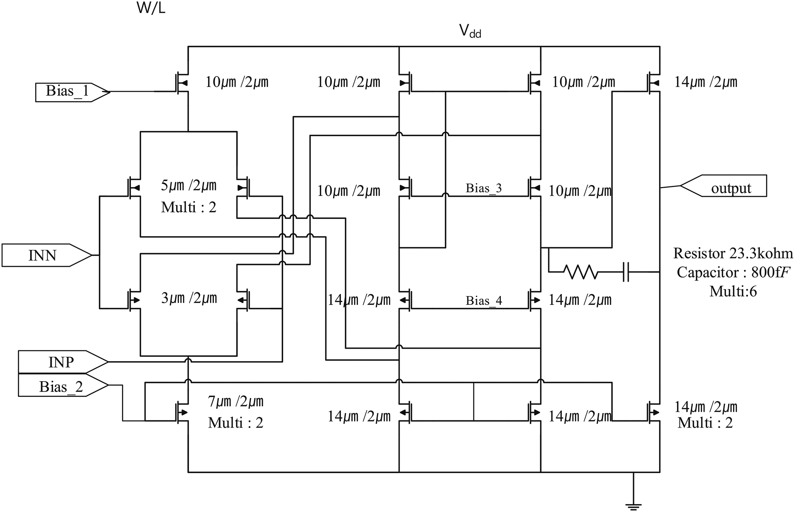
Schematic of rail-to-rail folded cascode amplifier.
Design of biphasic stimulator
A biphasic stimulator was implemented using the widely used H-bridge circuit. Generally, a high-voltage (HV) process injects a high-current amplitude into a stimulator circuit.19,20 However, because a specific process is limited, the amount of charge required for cell stimulation can be satisfied by using a PCM method and standard process. This setup enables the direction of current flow to the WE and CE to be controlled via the on/off switching of MOSFETs.21,22 In this arrangement, the H-bridge determines the direction of the current, and the amplitude of the current is controlled using an N-type MOSFET situated beneath the H-bridge, in conjunction with the current source connected to the OPAMP.23–25 Consequently, the amplitude of the injected current is influenced by the voltage stored in the capacitor, reflected in the output voltage of the OPAMP, and further modulated by Rex. To effectively simulate this system, we assumed a current pathway through identical electrodes and solutions on both sides, with the solution resistance set at 500

(a) Electrode-solution model and (b) model parameter (c) PCM method.
Simulation result
Result of switched capacitor structure
The simulation required four signals: two H-bridge-enabled signals (as shown by
Schematic of top cell.

Charge/discharge capacitor voltage according to the Si nanowire model
Result of amplifier
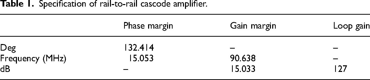
As mentioned previously, the designed amplifier was a rail-to-rail folded cascode amplifier. Its performance metrics, including the unit gain bandwidth, gain margin, and phase margin, are presented in Table 1. In this design, the accumulated voltage, which was derived from the current flowing through the nanowire, in the switched capacitor structure was used as the input for the amplifier. Subsequently, the voltage was regulated by adjusting the output of the amplifier. The adjusted output was connected to the gate of the MOSFET, which regulated the current flowing into the biphasic stimulator.
Specification of rail-to-rail cascode amplifier.
Comparative analysis of retinal prostheses.

Result of biphasic stimulator
The combined operation of a switched capacitor, amplifier, and other components drove the biphasic stimulator. The amplitude of the current flow between the WE and CE was controlled by connecting them to the MOSFET gate. In a biphasic stimulator, the direction of current flow was controlled by the

Current amplitude flow in WE-CE according to the capacitor charging voltage. CE: counter electrode; WE: working electrode.

System layout result.
Conclusion
In this study, we simulated a circuit to drive a stimulator to display its responsiveness to the photoreactivity of Si nanowires using the optical characteristics of the nanowires. This demonstrated the potential use of Si nanowires in retinal prostheses by translating variations in current influenced by the optical properties of the Si nanowires into changes in the current amplitude of the biphasic stimulator. The switched capacitor structure is essential in efficiently converting sensor-derived current into voltage, thereby regulating current flow through the WE and CE. When
Footnotes
Declaration of conflicting interests
The authors declared no potential conflicts of interest with respect to the research, authorship, and/or publication of this article.
Funding
The authors disclosed receipt of the following financial support for the research, authorship, and/or publication of this article: This research was supported by the MSIT (Ministry of Science and ICT), Korea, under the ITRC (Information Technology Research Center) support program (IITP-2024-RS-2024-00438239) supervised by the IITP (Institute for Information & Communications Technology Planning & Evaluation).