
Abstract
We review the past development of highly sensitive and selective gold nanoparticle (AuNP)-based assays of protein and DNA biomarkers for chip-based detection systems. The microfluidic systems, various assays, and preliminary laboratory results are shown. AuNP-based biodetection assays provide low detection threshold, offering promises for multiplexed diagnostics of many forms of disease markers.
Introduction
Over the past several years, a number of exciting advances have been made in the field of nanobio-diagnostics, resulting in assays that rival or surpass the selectivity and sensitivity of conventional detection methods.1, 2 These advances have the potential to dramatically change the way medical diagnosis and treatments are performed in the future. Through collaboration with Mirkin research group at the Northwestern University,1,3,4 we have been developing chip-based assays based on biobarcode assay (BCA) and, more broadly, gold nanoparticle (AuNP)-based assays. The BCA uses AuNPs functionalized with oligonucleotides (so-called bio-barcodes, which serve as surrogate targets and amplifying agents) and a target-recognition element, which may be an antibody for protein detection or a unique oligonucleotide sequence for nucleic acid detection. 1 The BCA also uses functionalized magnetic microparticles (MMPs), which are adorned with antibodies that bind to the target. In the presence of targets (protein or oligonucleotide molecules) in solution, the MMPs form a sandwich complex with the targets and AuNPs, which can be localized and collected under an applied magnetic field. The barcode oligonucleotide molecules are then chemically released, identified, and quantified.
The BCA is highly sensitive. In the benchtop format, the BCA has been shown to achieve low-attomolar sensitivity for protein analytes, up to five orders of magnitude lower than analogous enzyme-linked immunosorbent assay (ELISA) technology, the benchmark method for protein detection. The BCA also has exhibited high-zeptomolar sensitivity for nucleic acid targets, rivaling the PCR-amplification method, which requires thermal cycling. The BCA is also highly specific and capable of extensive multiplexing. Therefore, the BCA offers several unique diagnostic opportunities, including early disease detection, monitoring of disease recurrence, 5 and the possibility of simultaneous multiplexed analysis of a panel of disease markers.
Microfluidic systems should and would eventually replace the benchtop assay to achieve portability, automation, and simplicity of use. Our group has modified the benchtop BCA to adapt to the microfluidic and portable systems requirements. These adaptations are very important and often results in significant deviation from the benchtop predecessors. We have first developed a chip-based BCA. 6 Later, this method has been modified to become the surface-immobilized BCA (SI-BCA), 7 which is simpler than the original BCA and actually work only in the micro-fluid format. Meanwhile, various other detection schemes, such as electronic-gap detection 8 and mechanical resonance detection, have been developed at the proof-of-concept stage.
In terms of microfluidics, our past efforts include many components, including magnetic membrane valves,9, 10 magnetic stir bar mixers, 11 flow and channel filling sensors, 12 and integrated valves with soft O-ring seals. 13 We have also developed a multilayered modular microfluid architecture 14 for low-cost rapid prototyping of custom microfluid systems.
Assay Development
Chip-Based SI-BCA
The BCA was originally developed in a benchtop format. The established benchtop BCA protocol cannot be directly transferred to a chip-based format because of unique scaling, materials, and microengineering issues. We have successfully demonstrated a modified BCA that takes advantage of unique microfluid scaling and adjusts for the constraints of Lab-On-Chip (LOC) systems. 7
Chip-based BCAs developed thus far have used MMPs. However, there are a number of issues associated with executing this approach on chip. For example, because of the large volume difference between MMPs and the NP probes, it is very easy for NPs to become trapped in the packed bed of MMPs. In practice, this unintentional trapping increases the false-positive rate. Removing nonspecifically trapped AuNPs is not practical as it requires extensive wash protocols and substantially increases assay time (by nearly 30 min). Furthermore, the use of MMPs requires the use of switchable electromagnets for the on-chip instrument, increasing the complexity and cost of the system.
A simple alternative is to directly pattern the monoclonal antibodies on the walls of the microfluidic channels
7
(Fig. 1). In the presence of targets, the NPs would be bound to the channel wall through the target linker. Instead of forming an MMP—target—NP-sandwich in solution and then pulling the sandwich to the reactor sidewall using a magnetic field, the sandwich is formed at the reactor wall. This new SI-BCA protocol eliminates the need to use MMPs and reduces false-positive readings in microfluidic devices. It also reduces the complexity of the microfluidic system by eliminating the need for creating a magnetic field on demand.
Schematic diagram of the SI-BCA protocol. (A) The walls of the capture region are coated with antibodies. (B) Samples are flowed through the capture region. (C) The target molecules attach to the antibodies on the channel walls. (D) The target proteins are tagged with cofunctionalized-NPs containing polyclonal antibodies and unique barcode DNA oligonucleotides. (E) The barcode DNA is then released from the NPs and transferred to the detection region where the complementary sequence is patterned. Steps from F to H illustrate a scanometric detection protocol. (F) The barcode molecules attach to the complementary sequences in the appropriate regions. (G) Universal NP probes are attached to the barcode DNA. (H) The universal probes are silver stained to facilitate visualization in the visible spectrum. The red-colored channels represent the target capture region, whereas the green-colored channels mark the barcode detection region of the device. Dark blue lines are pneumatic control channels used for directing the flow of fluid.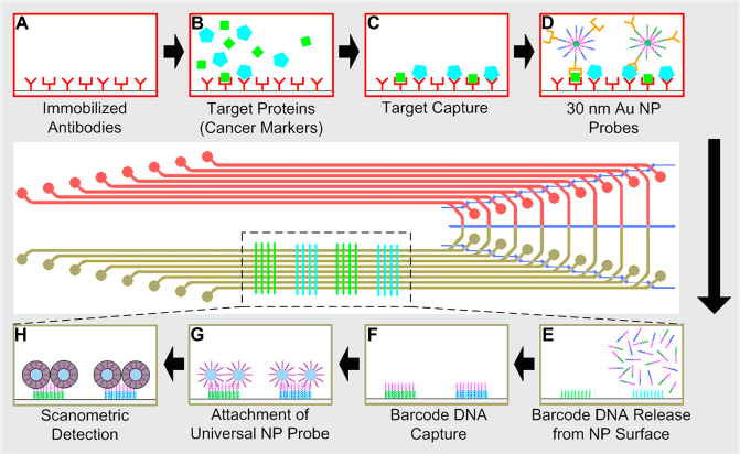
Electronic-Gap-Based Assay
The BCA can be quantified using a number of methods, including optical scattering,
15
electric gaps,
3
and Raman scattering. Electrical detection does not require bulky optical components and should result in less energy-hungry instruments. Using the dip pen nanolithography (DPN) technique, capture single-stranded DNAs (ssDNAs) are written inside 5- × 10-μm electronic gaps (E-gaps) on substrates (Fig. 2). The DPN-functionalized E-gaps can specifically hybridize to target ssDNAs in solution. Successful hybridization of the capture —target DNA complex is detected by the use of AuNPs carrying ssDNA, which also hybridize to the target ssDNA, followed by silver enhancement. The drop of resistance across the gaps because of the formation of metal nanoparti-cle—DNA complexes is measured over time and compared against characteristics of control gaps, which are either left un-functionalized or functionalized with noncomplementary capture ssDNA. This technique has potential for high-density multiplexed DNA assay chips. Multiplex detection of two different target ssDNAs in solution using DPN-functionalized electrical gaps on the same chip is demonstrated. The lowest detection limit is 10 pM. It should be noted that this number is lower than what was reported by Park et al. in Ref.
3
The difference is attributed to changes in the protocol (i.e., DPN functionalization vs droplet functionalization). We believe there is room for improvement in the future.
Schematic diagram of the E-gap biodetection scheme implemented in a microfluid channel.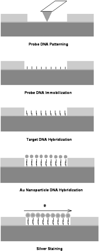
Pipetting is usually used to spot capture ssDNA molecules inside the electrical gaps of substrates. Spotting by pipetting may result in a large size functionalized area, typically 100 × 100 μm. Such large sizes of functionalization area are not amenable for the development of high-density multiplexed detection chips and consumes large amount of capture oligonucleotide material. Using pipette spotting, it is impossible to produce functionalization area below 10 × 10 μm. Therefore, it is advantageous to develop new functionalization techniques that overcome the aforementioned drawbacks of spotting methodology. 16
DPN is an emerging technique to fabricate nanoscale chemical patterns.17, 18 It uses a sharp scanning probe, or an array of scanning probes, to transfer chemical ink onto solid substrates. These inks include small organic molecules, peptides, proteins, oligonucleotides, and inorganic sol—gel. In this technique, the atomic force microscope (AFM) tip is brought into close proximity to the substrate under proper conditions. Ink biomolecules transport from the tip of an AFM to a substrate surface via a water meniscus. The typical dimension of biomolecule patterns on the substrates fabricated by DPN is micron or submicron size. Therefore, DPN can easily produce precise and user-defined patterns inside confined, micron-sized electrical gaps.
SEM micrograph of an E-gap after silver staining to close the circuit gap.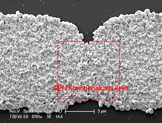
We investigated the effect of silver staining time on the differentiation of the detection gap and the control gaps next. The resistance of each gap and the differentiation among gaps is a function of staining time. We conducted a silver-staining time-course study for more than 30 min (Fig. 4). The chips used in the study contained two gaps functionalized with LT114 chip DNA; one gap functionalized with LT68 chip DNA and one gap with no chip DNA functionalization. Solution containing LT114 target DNA (at a concentration of 10 nM) was used in this time-course study. It can be observed from Figure 4 that when a proper nanoparticle-containing DNA hybridization complex is formed ([LT114 chip DNA-LT114 target DNA—AuNP probe]), a measurable drop in resistance is seen from 6 to 12 min silver-staining time. During this time, the control gaps containing noncomplementary chip DNA (LT68 chip DNA) or no DNA exhibit infinity resistance readings. In 26 min, nonspecific silver-staining of the gap containing LT68 chip DNA occurs as indicated by a drop in resistance, whereas the gap with no chip DNA shows no silver staining or measurable resistance even at 30-min staining time. This study shows the optimal time for silver staining to differentiate detection gaps and control gaps. Understaining (e.g., less than 6 min) will not differentiate various gaps, whereas overstaining (e.g., more than 20 min) will result in nonspecific detection as well.
Resistance change across a gap with respect for time. The gap with complementary functionalized DNA exhibits the most rapid change of resistance.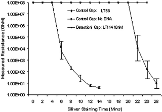
Mechanical Resonance Detection
The final step of the nanoparticles biodetection is a silver staining, which increases the mass of the overall chemistry assembly by a significant amplification factor. We are therefore interested in a mass-based detection method. One such possibility is to measure mass loading on a resonant cantilever and observe the frequency shift. Such a technique can be extremely useful compared with optical- or electromagnetic wave based techniques. It may also provide greater dynamic range when an array of cantilevers with different sizes and resonant frequencies are used (Fig. 5). Compared with the E-gap-based technique, the frequency shift and mass loading may yield more quantitative measurement.
A mechanical BCA assay. (A) Principle of mass loading and frequency shift. (B) Detailed view of molecular attachment to the cantilever. (C) Optical micrograph of a silicon nitride cantilever array. (D) Optical micrograph of a single crystal silicon cantilever array. (E—G) SEM of cantilever surfaces after exposure to 10 pM, I fM, and control fluid. (H) A typical frequency shift plot.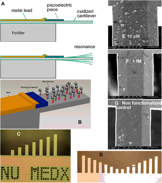
An array of cantilevers has been realized, made of both silicon nitride and single crystal silicon (Fig. 5C, D). Initial testing results using an array of single crystal silicon probe are shown in Figure 5E—G. Initial results show promise of low detection limit (10 fM). More results will be discussed in the future.
Microfluid Development
Advancement of microfabrication technology in the past few decades has enabled miniaturization and large-scale integration of complex systems. This has resulted in the availability of such products as analog/digital integrated circuits and powerful computers at affordable prices. The effects of miniaturization and integration reach far beyond the semiconductor industry. Micro- and nanoscale technologies are increasingly sought for purposes outside traditional electronic applications.
One such example is the microfluidic LOC. Microfluidic technology promises to automate macroscale, benchtop laboratory protocols and encapsulate them in low cost, portable systems. These systems benefit from reduced consumption of expensive reagents, precise manipulation of small volumes of fluid as low as a few picoliters, batch fabrication, and the ability to analyze a sample closer to the length-scale of the subjects of interest (e.g., cells, protein, DNA). Important examples of LOC applications include sample preparation, cell manipulation, biomolecular separation,19, 20 the PCR,19, 21 immunoassay-based detection,22, 23 and hybridization arrays.23, 24 Hence, LOCs have the potential to dramatically change the way biochemical analysis is performed for clinical diagnostics, environmental monitoring, pharmaceutical drug discovery, and chemical synthesis.
To successfully build an LOC, one must take into account a variety of different concerns, including biochemical compatibility, channel surface passivation/functionalization, optical transparency, ease of microfabrication, system integration, and the cost of development. Significant time and expertise are required to resolve often nontrivial issues.
A gap currently exists between the developers and potential users of microfluidic chips. Potential users, especially those in life sciences, generally do not have the means to manufacture or purchase custom microfluidic systems. Custom systems incur substantial costs because of both low-volume production and the long development time associated with creating highly functional devices.
From the developers’ perspective, two prevailing practices in LOC development contribute to the difficulties of building such a system. First, existing systems often use a monolithic approach, where chemical reactors, sensors, and actuators are integrated on a single chip. This requires a microfabrication process common to all components such that functionality may have to be compromised to build the device. Second, the components typically reside on a single plane, creating a need for elaborate channel routing to interconnect these components. Modifying one portion of monolithic and planar systems frequently entails rebuilding the entire system.
Our approach to narrow the gap lies in the introduction of a system-level microfluidic architecture that allows for rapid customization with low cost using materials satisfactory to both users and developers. The system reaches these goals by circumventing the obstacles encountered in conventional approaches.
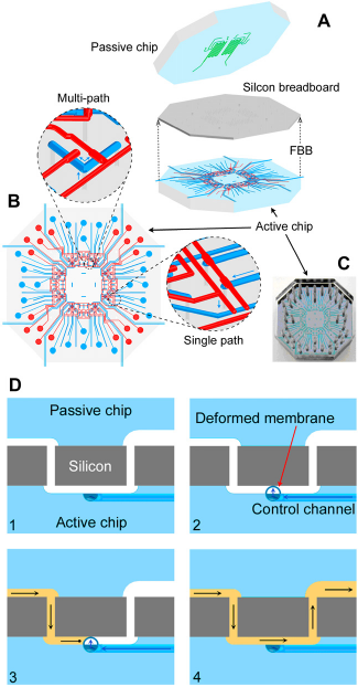
We developed a new LOC architecture that is conceptualized on two levels: A single chip level and a multiple chip module (MCM) system level (Fig. 6). At the individual chip level, a multilayer approach segregates components belonging to two fundamental categories: (A) Schematic diagram of a representative FBB consisting of electromechanical components and through-wafer fluidic connections. (B) A complete LOC can be built by bonding a passive fluidic chip with an FBB. The inset is a perspective view emphasizing the fluidic communication between components on two levels. (C) Different functions may be realized by deploying different passive chips on the same FBB. (D) Multiple chips can be interconnected to form a larger system at the MCM level. First-generation FBB implementation. (A) The system was assembled by reversibly bonding a passive polydimethylsiloxane (PDMS) chip to the FBB, which consisted of an active PDMS chip bonded to an oxidized silicon wafer with through-wafer holes. (B) Pneumatically actuated valves were formed at the crossing of the pneumatic control (red) and fluid (blue) channels on the active chip. Single valves may be used to control sample loading, whereas multiple valves can be used for multipath switching. (C) An optical micrograph of a single LOC. Holes were punched in the PDMS chip to provide pneumatic connection ports to the valve control channels. (Dl) Cross-sectional view of the LOC emphasizing the operation of a single valve. An empty channel is (D2) cutoff by a thin PDMS membrane actuated via pneumatic pressure. (D3) Fluid may be filled up to the closed valve as air escapes through the PDMS. (D4) Releasing the pressure in the pneumatic control line opens the valve and allows the fluid to continue flowing.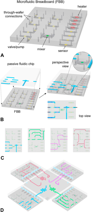
Conclusions
The AuNP is a versatile enabler of novel high-sensitivity and high-selectivity chemical assays for medical applications. We have developed various assays that are custom optimized for the microfluid system implementations. Some assays show unique performance characteristics that rival those of bench-top systems. Future work will focus on three performance aspects: (1) sensitivity and selectivity should be 100—1000 better than the best laboratory assay currently available in hospitals, (2) the assay must be reliable and repeatable, so it can be used for point of care and remote field applications, and (3) the assay, together with chips and control/readout systems, must be made at low cost.
Footnotes
Acknowledgments
Work discussed in this review has been supported by the United States National Science Foundation (Nanoscale Science and Engineering Center), The Department of Defense (DARPA Symbiotic Project), and the National Institutes of Health (NIH Center for Excellence in Cancer Nanotechnology).