
Abstract
Near-infrared (NIR) light sources are widely utilized in biological and medical imaging systems owing to their long penetration depth in living tissues. In a recently developed biomedical non-invasive cross-sectional imaging system, called optical coherence tomography (OCT), a broadband spectrum is also required, because OCT is based on low coherence interferometry. To meet these operational requirements, we have developed a NIR broadband light source by integrating self-assembled InAs quantum dots (QDs) grown on a GaAs substrate (InAs/GaAs QDs) with different emission wavelengths. In this review, we introduce the developed light sources and QD growth techniques that are used to control the emission wavelength for broadband emission spectra with center wavelengths of 1.05 and 1.3 μm. Although the strain-induced Stranski-Krastanov (S-K) mode-grown InAs/GaAs QDs normally emit light at a wavelength of around 1.2 μm, the central emission wavelength can be controlled to be between 0.9–1.4 μm by the use of an In-flush technique, the insertion of a strain-reducing layer (SRL) and bi-layer QD growth techniques. These techniques are useful for applying InAs/GaAs QDs as NIR broadband light sources and are especially suitable for our proposed spectral-shape-controllable broadband NIR light source. The potential of this light source for improving the performance of OCT systems is discussed.
Keywords
1. Introduction
1.1 Broadband light source required in OCT system
Near-infrared (NIR) light is commonly utilized in biomedical imaging systems owing to its long penetration depth in biological samples. In particular, NIR light of a wavelength of approximately 0.7–1.3 μm has a relatively long penetration depth in living tissue, and this well-known range, useful for cross-sectional imaging of biological samples, is referred to as the “optical window” [1]. As shown in Figure 1, the absorption of light by oxyhaemoglobin (HbO2) and water (H2O), which are the main components of tissue, is relatively low in the “optical window”, and is minimized at 1.05 μm. This wavelength is useful for imaging aqueous biological samples such as ophthalmic tissue. For non-aqueous tissues such as human skin, however, a wavelength of 1.3 μm is also useful for imaging because there is less absorption by HbO2 and less scattering in the biological samples.

Absorption or scattering of light in bio-materials as a function of wavelength in log-log scale Light absorption by oxyhaemoglobin (HbO2) and water (H2O) which are the main components of tissue, are minimized in the “optical window” [1].
Among the various biomedical imaging systems, optical coherence tomography (OCT), which can perform non-invasive cross-sectional imaging has been extensively developed over the last few decades, following the first report in the 1990s [2] As shown in Figure 2, OCT is based on low-coherence interferometry and the axial resolution of the OCT image depends on the center wavelength and bandwidth of the light source For instance when a light source emitting light with a Gaussian spectral shape centered at λ0 and a bandwidth of Δλ is used the axial resolution can be expressed as 0.44 λ02/Δλ [3], Thus a light source with a wider spectral bandwidth will result in a higher axial resolution in the OCT image Although the axial resolution also depends on λ0, it is necessary to ensure this wavelength is in the NIR range to obtain a large penetration depth in biological samples In addition some attention should be paid to the spectral shape of the light source so that clear OCT images are possible A spectrum containing large dips will have side-lobes in the Fourier-transformed power spectrum (coherence function) which leads to noise in the OCT images [3 4] Thus the features required for a light source suitable for high-quality OCT imaging of biological samples can be summarized as (1) broadband, (2) wavelength located in the appropriate NIR region and (3) spectral-shape controllable.

Schematic image of a (time-domain) OCT system
1.2 Broadband light source based on self-assembled InAs/GaAs quantum dots
OCT systems usually use a commercial semiconductor superluminescent diode (SLD) as the broadband light source. The SLD emits light with a lower coherence than that of a laser diode (LD) and higher output power than that of a light-emitting diode (LED) Typical bandwidths of SLDs are approximately several tens to 100 nm, resulting in a ∼10-μm axial resolution for OCT imaging. Although alternative light sources have been developed, SLDs have the advantages of being robust, compact and relatively cheap [5] However it is still important to develop SLDs that meet the three requirements for ideal OCT light sources The SLD device is usually based on a conventional light-emitting semiconductor material such as a quantum well, and it is not easy to broaden the bandwidth beyond 100 nm To overcome this difficulty an SLD based on an alternative material a self-assembled quantum dot (QD) was proposed [6] and has been studied intensively [7–21].
The QD a three-dimensionally quantum confined structure is a promising material for electronic and optical devices because of its unique configuration of electron states [22] For instance highly efficient light emission due to the delta-function density of states and low thermal sensitivity of the emission resulting from the high energy separation of the discrete states in a QD are some of the advantages The self-assembly of In(Ga)As QDs on a GaAs substrate [23–25] is a well-known method of realizing QD structures and has been extensively studied for both fundamental physics and device applications [26–28]. The QDs are derived from strain induced by a lattice mismatch between the deposited material and substrate (S-K growth mode). Figure 3 shows a typical atomic force microscopy (AFM) image and room temperature (RT) photoluminescence (PL) spectrum obtained from an InAs QD ensemble grown on a GaAs (100) substrate.

(a) AFM image of InAs-QDs grown on a GaAs substrate. (b) PL spectrum obtained from InAs-QDs embedded in a GaAs matrix at RT (red curve).
There are two peaks with inhomogeneous broadening in the PL spectrum, which originate from the recombination of the e-/h-ground states (GS) and the first excited states (ES) of the QDs. The S-K growth mode of the QDs yields a distribution of the size and composition of the QD, resulting in the broad emission lines of the GS and ES recombination. This inhomogeneity is not appropriate for laser applications, but it is suitable for a broadband light source. We note also that the emission wavelength is at approximately 1.2–1.3 μm. These features match those required for OCT light sources in skin tissue imaging.
As mentioned, SLDs based on InAs QDs have been widely studied and reported to exhibit broadband and strong emission with a combination of GS and consequent ES stimulated emissions. These QD properties are more promising for OCT applications than those of the conventional SLD devices, particularly if multiple InAs QDs layers with different emission wavelengths (“chirping” the QD layers) are used.
1.3 Proposal for spectral-shape-controllable broadband light source based on monolithically grown multi-color InAs QDs
An NIR broadband light source based on multiple-stacked self-assembled InAs QD layers with different emission wavelengths has been realized. However, obtaining the desired spectral shape involves complicated QD growth techniques such as the chirping technique, and some optical gain is sacrificed since reabsorption occurs between the stacked QDs. To overcome these problems, we proposed the utilization of parallel QD ensembles grown monolithically on a GaAs substrate [29]. Figure 4 shows a schematic of the proposed light source, which consists of multiple InAs QD ensembles with different emission wavelengths and employs a ridge-type waveguide (RWG) structure. The RWG is used to combine the emission spectra of the different QD ensembles. In addition, providing individual excitation power for each QD is possible in order to tailor the spectral shape. Furthermore, any emission power losses that may occur because of absorption by QD ensembles with lower band gap energies can be avoided by arranging the ensembles in order of increasing band gap energy along the waveguide.

Schematic drawing of a spectral-shape-controllable broadband light source based on monolithically grown multiple QD ensembles
In this review, we first introduce our monolithic growth technique to realize the proposed spectral-shape-controllable NIR broadband light sources. The broadband spectrum of the combined multiple QDs and controllability of the spectral shape have been demonstrated [30]. Then, the techniques for controlling the central emission wavelength of the InAs QDs grown on GaAs are described in sections 3 and 4. These are based on previously reported bi-layer QD growth and In-flush techniques, which can be applied to broadband light sources centered at 1.3 and 1.05 μm, respectively. Finally, we introduce EL data obtained from stacked QD layers with controlled emission wavelengths. These results are applicable for the monolithic growth technique, and enable the integration of multiple QD ensembles, providing the possibility to span the 0.9–1.4 um range. We discuss the potential of these approaches for realizing novel NIR broadband light sources that meet the three requirements for ideal OCT light sources.
2. Light source based on monolithically grown InAs QD ensembles
2.1 Growth method for monolithic multi-color InAs QDs using a rotational metal mask
To realize the proposed light source, we developed a growth method for monolithic QDs with different emission wavelengths. We previously developed the selective area growth (SAG) of InAs QDs on GaAs during conventional molecular beam epitaxy (MBE) with a metal mask (MM) [31]. Based on the MM/MBE method, we developed a new rotational MM for the SAG of four QDs, as shown in Figure 5 [32].
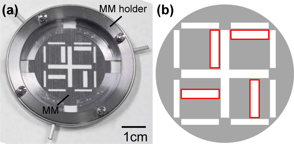
(a) Photograph of a rotational MM attached to a holder. (b) Schematic drawing of an MM. Open windows for the selective area growth are indicated in red.
An MM made of Ta was attached to a mask holder. The MM holder can be mounted on and removed from a substrate in an ultra-high-vacuum (UHV) environment. The MM has open windows for supplying the molecular beams to selective areas on the substrate during the MBE growth. In addition to four windows (2 mm × 8 mm) for SAG (indicated in red), a large cross-shape window in the center of the mask is prepared for in situ observation of reflection high-energy electron diffraction (RHEED) patterns, which enables the optimization of the growth temperature. The electron beam for RHEED is incident into tunnels formed in the frame of the MM holder and is diffracted in the central region of the substrate. Eight additional rectangular slits positioned at the edges of the mask are included to reduce the thermal gradient of the sample surface caused by heat reflection from the MM. These slits can also be used to maintain the As pressure between the MM and substrate surface by ventilation of the As vapour through the slits.
During the SAG, the open windows define different angles to the molecular-source cells. Thus, regions deficient in reagent supply (shadow effect) should be considered. Such shadow effects can be prevented by reducing both the thickness of the MM and the distance between the MM and the substrate. However, an excessively thin MM may result in deformation of the MM, and having the MM too close to the substrate will significantly influence the growth conditions because of excessive heat reflection from the MM and low As pressure beneath the MM. Therefore, we optimized the thickness of the MM to 0.2 mm and set the distance between the MM and substrate to 0.1 mm. We have confirmed that under these conditions the shadow effect is negligible [31].
The MM can be rotated in the UHV chamber, and a rotation of 90° moves the open windows on the rotationally asymmetric pattern to define four different neighbouring SAG regions. By repeating this operation four times, we obtain four parallel QD growth regions on the substrate. In each case, we grew QDs with 2.0–2.6 monolayer (ML) of InAs after the growth of a GaAs layer that was several tens of nanometers thick. To vary the emission center wavelength of each QD ensemble, we deposited a strain-reducing layer (SRL) [33] on the QDs with different thicknesses. As shown in Figure 6, the deposition of SRLs with thicknesses of 0.0, 1.3, 2.4 and 4.1 nm realized the monolithic growth of four QD ensembles (QD1–4) with different emission peak wavelengths [32].

Schematic drawing of the SAG of multiple QDs with different emission wavelengths by using a rotational MM. (Reprinted with permission of Ref. 32, Ozaki N, et al., IEICE Trans. Electron. E95-C: 247–250 (2012). Copyright IEICE).
Figures 7 (a) and (b) show a typical plan-view PL intensity map and RT PL spectra obtained from the grown wafer, respectively. The PL intensity map, which is shown as a grayscale of the PL intensity integrated over emission wavelengths of 1100 nm to 1400 nm, shows four rectangular emission areas in each quadrant of a wafer. These areas correspond to the grown areas via the MM, as schematically shown in Figure 6; each quadrant includes four rectangular QD1–4 growth regions, which are parallel, and in various orders. Each PL spectrum obtained from each area exhibits a well-controlled emission peak wavelength, as typically shown in Figure 7(b). These results demonstrate that the SAG of the QDs and the control of the emission peak wavelength were executed as planned. A 120 nm shift in the emission peak wavelength with an increase in the SRL thickness was achieved, and the total bandwidth of the GS emissions of the QDs was approximately 160 nm.

(a) PL intensity map obtained from a wafer, including multiple QD ensembles. (b) PL spectra obtained from the QD growth regions. (Reprinted with permission of Ref. 32, Ozaki N, et al., IEICE Trans. Electron. E95-C: 247–250 (2012). Copyright IEICE).
With the assumption that the ES emissions will contribute to the spectrum at a high drive current, as described in section 5, a bandwidth of over 200 nm can be expected in a practical SLD. As these QDs are introduced into an RWG as shown in Figure 4, the spectral shape can be tailored by controlling the drive current for each QD ensemble and changing the peak intensities for the GS and ES emission lines of the multiple QD ensembles.
2.2 Demonstration of spectral-shape control using monolithic grown multi-color InAs QDs
To demonstrate the feasibility of the grown multiple QDs as a spectral-shape-controllable light source, an RWG that included the QD ensembles was fabricated. As shown schematically in Figure 8, a 200-nm thick active layer including SA-grown multiple QDs with different emission wavelengths was grown with 1.5-μm thick upper and lower cladding layers of Al0.35Ga0.65As on a GaAs (001) substrate. The active layer consists of GaAs layers and three stacked InAs QD layers with SRLs of different thicknesses grown in four selective areas (QD1–4) using the rotational MM method. The distance between each QD layer was 30 nm, and the upper cladding layer was capped with a 20-nm thick GaAs layer to prevent oxidization.

Schematic images of RWG structure including multi-color QDs in an active layer. (Reprinted with permission of Ref. 30, Ozaki N, et al., Appl. Phys. Lett. 103, 051121 (2013). Copyright AIP).
As shown in Figure 9, straight RWGs were fabricated using photo-lithography and inductively coupled plasma reactive ion etching (ICP-RIE), and the ends of the RWG were cleaved. The RWG was approximately 8 mm in length to include all the selective areas of the multi-color QDs. The height and width of the RWG were approximately 1.4 and 5 μm, respectively. To characterize the emission spectra through the RWG, we employed a micro-PL system that can excite two different regions in the RWG simultaneously, with two independent He–Ne lasers focused to a spot size of approximately 10 μm. The excitation power density of the lasers can be varied independently up to approximately 2 kW/cm2. The emission spectra exiting the RWG were detected with an InGaAs array detector attached to a monochromator through an objective lens (20×; numerical aperture (NA) = 0.40). All the PL measurements were performed at RT.
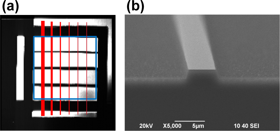
(a) PL intensity map obtained from a region for the RWG fabrication. Red lines indicate planned straight RWGs including multiple QDs. (b) SEM image of a fabricated RWG.
Figures 10(a) and 10(b) show the spectra obtained by exciting regions QD1 and QD4 and regions QD2 and QD3, respectively. The solid black lines indicate the emission obtained with a variation in the excitation power density for QD1 (QD2), while maintaining a constant excitation power for QD4 (QD3). The obtained emission spectra exhibit combinations of each QD emission spectrum, shown by the colored line, and the spectral shapes vary with changes to the excitation power. In Figure 10(a), the excitation power of the laser for QD1 was increased by approximately 1.25 and 1.50 times with respect to the lowest excitation power, while the excitation power of the laser for QD4 was fixed. In Figure 10(b), the power for QD2 was increased by 1.18 and 1.76 times with respect to the lowest excitation power, while the excitation power for QD3 was fixed. An increase in the PL intensity in each QD region in response to an increasing excitation power was seen, and independent control of the emission intensity from each QD in the combined spectrum was demonstrated.
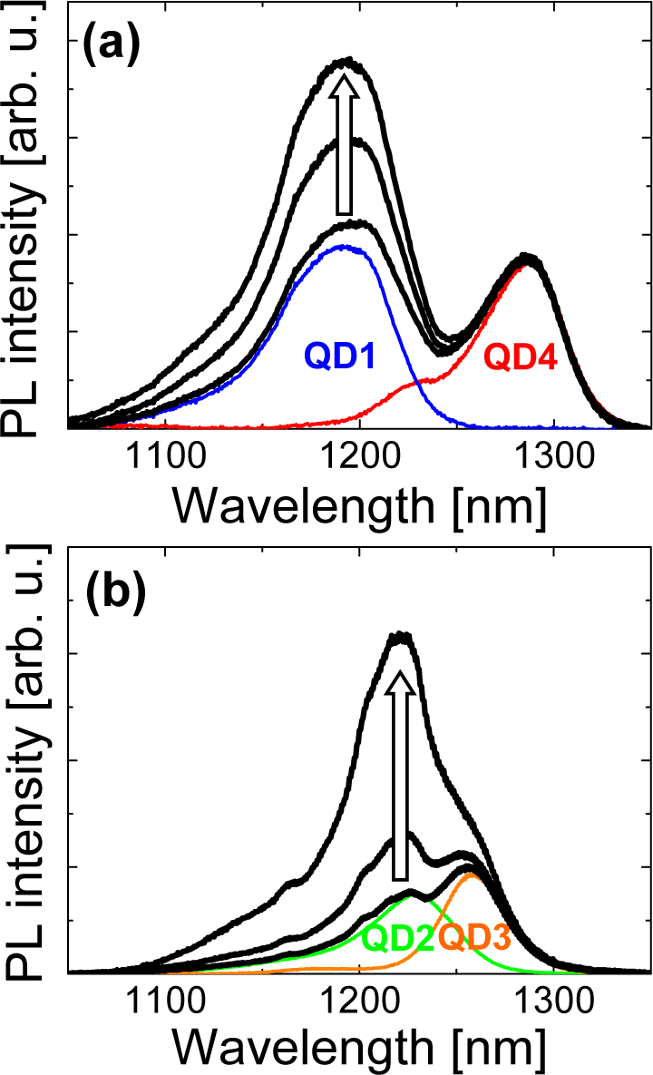
PL spectra obtained through the RWG by exciting (a) the QD1 and QD4 regions and (b) the QD2 and QD3 regions with a variable excitation power density. (Reprinted with permission of Ref. 30, Ozaki N, et al., Appl. Phys. Lett. 103, 051121 (2013). Copyright AIP).
These results demonstrate the feasibility of our proposed light source based on monolithically grown multi-color QD ensembles; the emission spectra of monolithically grown QD ensembles can be combined through an optical waveguide, and the spectral shape can be tailored by controlling the excitation power for each QD ensemble.
3. Bi-layer QD growth for extending emission wavelength centered at 1.3 μm
As described in section 2, the insertion of an SRL is effective for extending the emission wavelength of InAs/GaAs QDs and results in broadband emission.
However, there is a limitation to the extension via the SRL; the emission wavelength saturates at approximately 1.32 μm in our experiments [34]. For biomedical OCT applications, a broadband light source centered at 1.3μm is often used, because a large penetration depth in non-aqueous tissues can be obtained as described in section 1, and substantial commercial optical components are available in the wavelength range, which corresponds to telecommunication uses. Thus, developing a method to extend the emission wavelength beyond 1.3 μm is necessary. In this section, we introduce a QD bi-layer growth technique, which is a previously reported method that can be applied for our developed broadband NIR light source based on monolithically grown multi-color QDs. Our experiments have demonstrated that the emission wavelength of the bi-layer QDs has been well controlled to remain between approximately 1.2 and 1.4 μm though optimizing the bi-layer QD growth conditions [35].
3.1 Bi-layer InAs/GaAs QDs
Various methods for extending the emission wavelength of InAs/GaAs QDs in addition to SRL insertion have been investigated, because telecommunications technology also requires the use of light with a 1.31 or 1.55 μm wavelength. For instance, reducing strain between substrate and QDs by depositing a thick metamorphic InGaAs or GaAsSb buffer layer before the QD growth [36, 37] and capping the QDs with an In(Ga)As layer incorporating N or Sb [38, 39] have been reported to be effective methods for extending the emission wavelength. However, these methods require a thick buffer layer or a highly developed growth technique for doping N or Sb. Such conditions are inconsistent with those for the monolithic growth of InAs QDs on a GaAs substrate with the rotational MM method described in section 2.
A growth method for QD alignment along the vertical direction using a surface-stress in a stacked multiple QD layer structure was reported [40, 41]. This method has also been utilized in the strain effects of a closely stacked QD bi-layer for enlarging the QDs in the upper layer [42]. Optimizations of growth conditions enable the control of emission wavelength of the QD bi-layer structure, and a number of studies have reported the achievement of longer emission wavelength of InAs/GaAs QDs [43–48]. This alternative method for enlarging QDs and extending the emission wavelength without a thick buffer layer and dopants should be suitable for our proposed broadband light source based on the integration of QDs monolithically grown with different emission wavelengths.
Figure 11(a) shows a schematic illustration of the bi-layer InAs QDs. The first (lower) layer consisting of InAs-QDs, referred to as the seed-QDs, was grown on a GaAs layer. A GaAs spacer layer with a thickness of approximately 10 nm was then grown on the seed-QDs, and the second (upper) layer consisting of InAs-QDs, referred to as the active-QDs, was grown on the spacer layer. The surface of the spacer layer for the active-QDs' growth has a strain distribution due to the underlying seed-QDs, and the supplied InAs migrates along this surface and tends to assemble at positions above the seed-QDs [40]. Thus, enlarged active-QDs form above the seed-QDs, as shown in Figure 11(b). Since the active-QDs are larger than the seed-QDs, the energy level of GS of the seed-QDs is higher than that of the active-QDs. Thus, excited carriers will be transferred into the active-QDs, and light emission predominantly occurs between the hole and electron of the GS in the active-QDs. By considering the large separation between both QDs with a spacer thickness of 10 nm, the carrier transfer from seed-QDs to active-QDs can be due to carrier tunnelling [49, 50], rather than the formation of molecular states by the hybridization of electron and hole wavefunctions of both QDs, as reported in the case of closely stacked QDs or where a high electrical field is applied [51].

(a) Schematic image of a QD bi-layer. (b) Cross-sectional transmission electron microscopy (TEM) image of a bi-layer QD.
3.2 Optimized growth conditions for bi-layer InAs/GaAs QDs
To use the bi-layer InAs/GaAs QDs to extend the emission wavelength, we investigated the dependence of the emission wavelength of the bi-layer QD sample on various growth conditions: (i) the InAs deposition amount for the active- and seed-QDs and (ii) the growth temperature of the seed-QDs. In addition, the dependence on variation of the capping layer of the active-QDs was also studied. The grown QDs were characterized by AFM and PL measurements at RT. We grew two bi-layer QD structures in one sample; one on the top surface for the AFM observations, and another buried in the GaAs sandwiched by Al0.3Ga0.7As layers for the PL measurements. These bi-layer QDs were grown under the same growth conditions. For the PL measurements, an 80-mW He–Ne (λ = 632.8 nm) excitation laser was employed. The power density of the excitation laser was approximately 100 W/cm2.
3.2.1 InAs depositions for active- and seed-QDs
Initially, QD bi-layer structures were grown using conventional growth conditions optimized for the growth of high-density, high-quality QDs: an amount of 2.6 ML InAs deposition and a growth temperature of approximately 480 °C. After the seed-QDs were grown under these conditions, we grew (at the same temperature) active-QDs with varying amounts of InAs from 3.0 to 3.8 ML. The emission peak wavelengths of the resulting samples, shown in Figure 12(b), were 1.23–1.25 μm, which were slightly extended in accordance with an increase in the InAs deposition for the active-QDs. The AFM images in Figure 12(a) showed that the number of coalesced QDs increased and the density of regular (not coalesced) QDs decreased with an increase in the InAs deposition from 3.6 × 10¹⁰ to 1.9 × 1010 cm−2. In fact, the PL intensity of the emission peak continuously decreased (∼20 %) with the increase in the InAs deposition.

(a) AFM images, measured density and average sizes of active-QDs grown with different InAs depositions. (b) PL spectra obtained from the samples shown in (a). (Reprinted with permission of Ref. 35, Ozaki N, et al., J. Cryst. Growth 378, 553 (2013). Copyright Elsevier).
In addition, an emission peak at a shorter wavelength between 1.15 and 1.18 μm and a higher intensity than that from a single InAs-QDs layer appeared in the PL spectra. This may be attributed to emission contributions from the seed-QDs, whose GSs are not resonant with the ESs of the active-QDs. These results indicate that excess InAs deposition results in the production of coalesced QDs rather than enlarging the active-QDs, and incomplete bi-layer structures are formed. We considered this to be due to the high density of the seed-QDs. As shown schematically in Figure 13, highly dense seed-QDs create overlapping strain fields that would prevent InAs supply for the enlargement of active-QDs. Thus, reducing the density of the seed-QDs will optimize the strain distributions and result in enlarged active-QDs sizes, although the density of the active-QDs will also be lower.
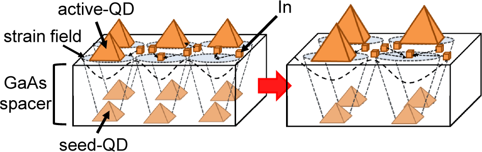
Schematic images of active-QDs on seed-QDs grown with different densities of seed-QDs. Reducing the seed-QDs' density can result in an enlargement of the active-QDs.
Hence, we subsequently fixed the InAs deposition amount for the active-QDs to 3 0 ML to avoid the formation of coalesced QDs, and grew seed-QDs with a reduced amount of InAs deposition. Figure 14(a) shows AFM images of the active-QDs grown on seed-QDs with different InAs deposition amounts (2.6 and 2.0 ML).

(a) AFM images of active-QDs on seed-QDs grown with different amounts of InAs deposition, 2.6 and 2.0 ML. (b) Comparison of the PL spectra of the samples shown in (a). (Reprinted with permission of Ref. 35, Ozaki N, et al., J. Cryst. Growth 378, 553 (2013). Copyright Elsevier).
Reducing the amount of InAs supplied for the seed-QDs' growth resulted in an increase in the mean height of the active-QDs from 5 6 to 6 1 nm while the active-QDs' density decreased from 3 6 × 10¹⁰ to 2 9 × 1010 cm−2 The PL peak wavelength was also red shifted from 1 23 to 127 μm as shown in Figure 14(b) Note that the emission intensity at the shorter peak wavelength decreased and that the emission at the longer wavelength was dominant This indicates that the bi-layer QD structure was well formed and light emission was dominated by the active-QDs, in this case The reduction in the InAs supplied to form the seed-QDs could cause a decrease in the seed-QDs' density and expand each strain field induced by a seed-QD on the surface for the growth of an active-QD This resulted in a decrease in the number of nucleation sites for the active-QDs and enlargement (ripening) of the active-QDs, as shown schematically in Figure 13 This assumption was explored through AFM observations of seed- and active-QDs grown with the same conditions as described in section 3.2.3.
3.2.2 Growth temperature of seed-QDs
We also investigated the dependence of the size and emission wavelength of the active-QDs on the growth temperature of the seed-QDs. In general, the QD density decreases and the QD size increases with an increase in the growth temperature [52]. Thus, we expect an increase in the growth temperature of the seed-QDs to result in larger active-QDs and extend the emission wavelength, as was seen for a decrease in the InAs deposition for the seed-QDs.
Figure 15(a) shows AFM images of the grown active-QDs for different growth temperatures of the seed-QDs: 473, 490 and 500 °C. The active-QDs were grown at approximately 480 °C. As seen in Figure 15(a), the density of the active-QDs decreased and the mean size of the active-QDs increased with an increase in the growth temperature of the seed-QDs. The wavelength of the PL emission peak was red shifted to 1.32 μm with an enlargement of the QDs, as shown in Figure 15(b). This center wavelength was extended by approximately 100 nm compared to that of InAs/GaAs QDs grown conventionally. These results also support the proposition that a lower seed-QD density will optimize the spatial spreading of the strain field induced by the seed-QDs and result in larger active-QDs and longer emission wavelengths.

(a) AFM images of active-QDs on seed-QDs grown at different growth temperatures. The seed-QDs were grown at 473, 490 and 500 °C. (b) Comparison of the PL spectra of the samples shown in (a). (Reprinted with permission of Ref. 35, Ozaki N, et al., J. Cryst. Growth 378, 553 (2013). Copyright Elsevier).
3.2.3 Density and average size of seed-QDs and active-QDs grown with the growth conditions
To explore the assumption that a lower seed-QD density results in larger active-QD growth, we measured and compared the density and the average sizes of seed-QDs (single-layer QD) and active-QDs (bi-layer QD) grown independently with various conditions. Figure 16 summarizes AFM images of the seed- and active-QDs. The density of seed-QDs decreased with decrease in amount of InAs deposition and increase in growth temperature. In accordance with the decrease in the density of seed-QDs, the average height of active-QDs was confirmed to have increased from 5.6 to 7.0 nm.

AFM images of active-QDs and seed-QDs grown at different growth conditions: InAs deposition and growth temperature for seed-QDs
Therefore, we conclude that lowering the density of the seed-QDs by increasing the growth temperature is significant for increasing the size of the active-QDs and extending the emission peak wavelength beyond 1.3 μm. The PL intensity was observed to decrease with the extension of the emission wavelength. This probably reflects the lowering of active-QDs' density in accordance with the seed-QDs' density.
3.3 Further extension by introducing an InGaAs capping layer for active-QDs
To further extend the emission wavelength of the QD bi-layer, we examined the dependence of the emission wavelength on the nature of the capping layer of the active-QDs. Compared to a GaAs capping layer, an InGaAs capping layer is expected to release strain in a similar way to the SRL effect described earlier. We compared the PL spectra obtained from (i) a single InAs-QD layer, (ii) a bi-layer QD sample capped with a GaAs layer, and (iii) a bi-layer QD sample capped with a 5-nm thick In0.2Ga0.8As layer and a GaAs layer, as shown in Figure 17(a). These bi-layers QD samples were embedded after being grown under the same conditions as the QDs that yielded the longest emission wavelength; the seed-QDs were grown with a 2.0 ML InAs deposition at 500 °C and the active-QDs were grown with a 3.0 ML InAs deposition at 480 °C. As shown in Figure 17(b), the InGaAs capping layer extended the emission wavelength. The longest PL peak wavelength of 1.38 μm was achieved with the QD bi-layer growth with an InGaAs capping layer deposition, and this wavelength is approximately 60 nm longer than that of the QD bi-layer capped with GaAs. Compared to the GaAs capped, single InAs QD structures, an extension of approximately 130 nm was achieved. Regarding the PL intensity, a decrease with InGaAs capping compared to GaAs capping was observed. This suggests that a reduction of the optical quality of the QDs with an InGaAs capping layer and further optimizing the conditions for the growth of the InGaAs capping layer is necessary. The dependence of the optical properties of bi-layer QDs on the capping layer is now under investigation and will be reported.

(a) Schematics of (i) a single InAs/GaAs QD layer, (ii) a bi-layer InAs QDs capped with GaAs and (iii) a bi-layer InAs QDs capped with 5-nm thick In0.2Ga0.8As and GaAs. (b) PL spectra obtained from the samples (i)–(iii). (Reprinted with permission of Ref. 35, Ozaki N, et al., J. Cryst. Growth 378, 553 (2013). Copyright Elsevier).
In summary, bi-layer QD growth is very promising for extending the emission wavelength of the InAs/GaAs QDs beyond 1.3 μm. The simple growth procedures outlined here are suitable for broadband light sources based on multiple QDs monolithically grown on a GaAs substrate. By optimizing the growth conditions, an emission spectrum centered at 1.3 μm with a bandwidth of approximately 200 nm can be expected.
4. Broadband light centered at 1.05 μm based on In-flushed InAs-QDs
As described in section 1, light with a center wavelength of 1.05 μm is recognized as an alternative probe for aqueous tissue, such as the human eye, because of the long penetration depth in biological samples [53]. To adjust the emission wavelength of conventional InAs/GaAs QDs, which emit approximately 1.2–1.3 μm, to the 1 μm regime, the In-flush technique, which was previously developed for QD height control [54], can be utilized [55–59]. In this section, the wavelength control technique is introduced and the potential of the obtained QDs as a broadband light source for OCT is discussed.
4.1 In-flushed InAs/GaAs QDs
The In-flush technique was initially reported as a height control method for self-assembled QDs to improve the uniformity of the dots [54]. As shown schematically in Figure 18, the technique enables the precise height control of InAs QDs by changing the thickness of the GaAs layer, partially capping the InAs QDs.
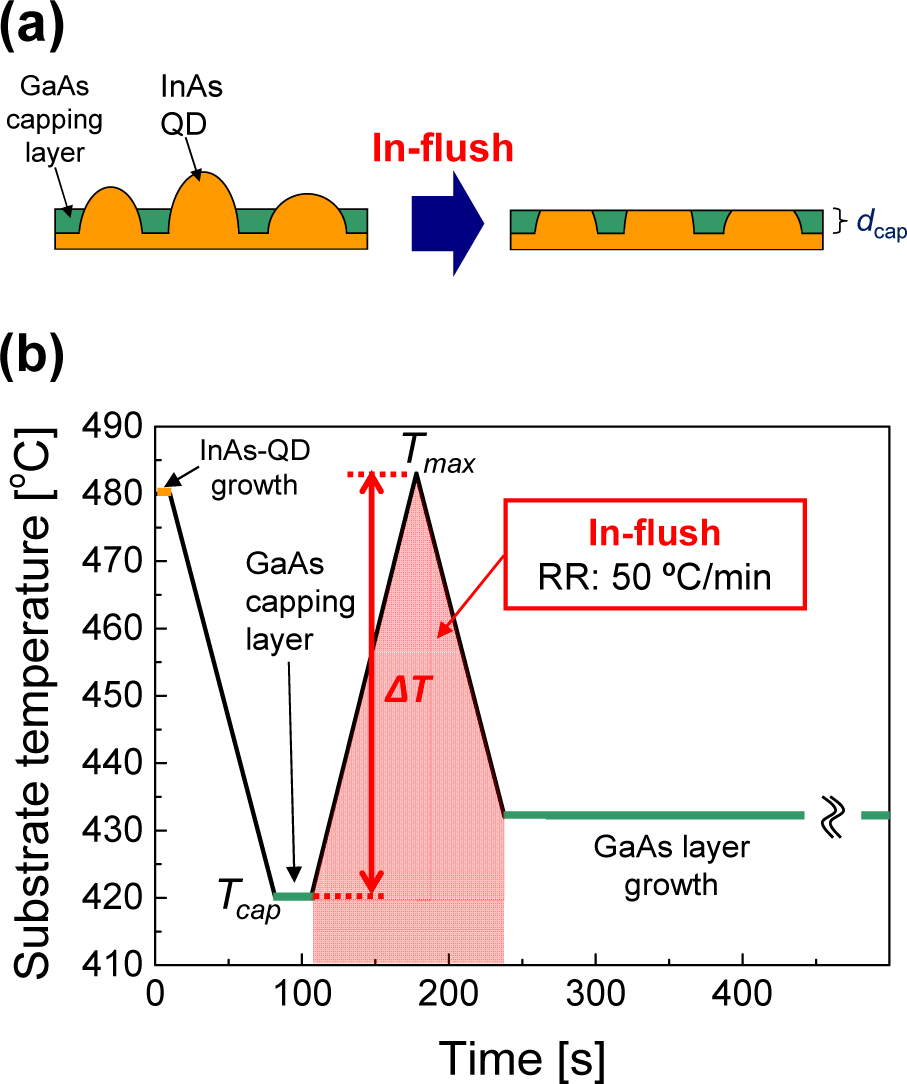
(a) Schematic image of the In-flush process (b) Time sequence of the In-flush process in our experiments.
After the QD growth on the substrate GaAs partial capping layers with a specific thickness (dcap) are grown on the QDs The substrate temperature is then rapidly increased and decreased to evaporate the excess QDs over the capping layer resulting in QDs with a height controlled by dcap This method can be easily applied to the emission wavelength control of InAs QDs grown on a GaAs substrate We have grown In-flushed InAs/GaAs QDs that emit light at a wavelength of around 1 05 μm to verify the effectiveness and applicability of the technique for the fabrication of a broadband light source Furthermore we have investigated the dependence of the emission properties of the In-flushed QDs on the annealing temperature of the In-flush process [58].
All the samples were grown on a Si-doped (100) GaAs substrate by MBE A GaAs buffer layer approximately 300 nm in thickness was grown first and an InAs-QD layer was grown via conventional S-K mode growth with 2 ML of InAs deposition. The InAs-QD layer was sandwiched between 30-nm thick GaAs spacer layers and 10-nm thick Al0.3Ga0.7As barrier layers for confining the charge carriers. The growth temperature of the QDs was approximately 480 °C. During the In-flush process shown in Figure 17(b), GaAs partial capping layers with various thicknesses (dcap = 1.0–5.1 nm) were grown on the QDs at a temperature (Tcap) of ∼420 °C, followed by a rapid increase in the temperature to evaporate the excess QDs over the capping layer. The substrate temperature was then rapidly reduced to approximately 420 °C soon after the maximum temperature (Tmax) was reached. The ramp rates (RRs) of the increase and decrease in the substrate temperature were above 50 °C/min. The total time interval for the In-flush was approximately 2–3 min. To investigate the dependence of the QD emission properties on the annealing temperature, we varied the increase in the temperature (ΔT = Tmax – Tcap) from 33 to 80 °C. During the entire growth, including the In-flush process, an arsenic flux of 2 × 10⁻⁵ Torr continuously irradiated the sample.
Figures 19(a) and (b) show AFM images of the as-grown and In-flushed InAs-QDs, respectively. These QDs were grown separately under identical QD growth conditions. For the In-flushed InAs-QDs, a 1.2-nm thick GaAs capping layer was deposited, and ΔT was approximately 60 °C. The mean lateral size and height of the as-grown QDs were approximately 40 and 5 nm, respectively, and the QD density was estimated to be 4.6 × 1010 cm−2.
By comparing the AFM images of the as-grown and In-flushed samples, it can be seen that the In-flushed sample surface is smoother than that of the as-grown QDs. The average roughness height was measured to be 1.7 nm for the sample shown in Figure 19(a) and 0.46 nm for the sample shown in Figure 19(b). During the In-flush process, it is likely that the In atoms in the QDs above the GaAs capping layer migrated on the surface, and as a result, the protruded QDs were flattened. HRTEM observations also demonstrated the height reduction using the In-flush technique. Figure 19(c) shows a typical cross-sectional HRTEM image of an embedded QD, which was In-flushed under the same conditions as those used for the QDs shown in Figure 19(b). The height of the InAs-QD, indicated by the arrow, was estimated to be 1.2 nm using the GaAs (100) lattice spacing as a reference. This is equal to the thickness of the capping layer, and thus it can be concluded that the In-flush was successfully carried out.

AFM images of (a) the as-grown InAs-QDs and (b) the In-flushed QDs. (c) Cross-sectional HRTEM image of the In-flushed QD.
4.2 Emission wavelength and intensity control of In-flushed InAs/GaAs QDs
We have also grown In-flushed QDs with various dcap values to control the emission wavelength. Figure 20 summarizes the variation in dcap and the corresponding peak wavelengths of the measured samples A to J. The PL spectra obtained at RT demonstrate that the PL peak wavelength can be controlled in the range ∼1.22–0.95 μm for the selected dcap values. The maximum blue shifted wavelength of the as-grown InAs QDs was approximately 270 nm, which indicates that an emission spectrum centered at 1.05 μm with a bandwidth of approximately 200 nm can be obtained using a combination of In-flushed QDs.

PL spectra of the In-flushed QDs with different GaAs capping layer thicknesses (dcap). (Reprinted with permission of Ref. 58, Hino Y, et al., J. Cryst. Growth 378, 501 (2013). Copyright Elsevier).
The results demonstrate the suitability of using the In-flush method for realizing a QD-based broadband light source with a center wavelength of 1.05-μm. However, it should be noted that the emission intensities tend to decrease with a decrease in dcap. This is thought to be due to the introduction of non-radiative centers (defects) at the interface between the QD and GaAs capping layer during annealing in the In-flush process, rather than a reduction in the carrier confinement. To examine the decrease in the emission intensity in more detail, we investigated the dependence of the QD emission properties on the annealing temperature (ΔT) for the In-flushed samples.
Figure 21(a) shows a plot of the variation in the PL intensities and peak wavelengths of the samples for a given dcap value of 2.0 nm, annealed at different values of the ΔT in the range of 33–80 °C. The results indicate that reducing ΔT from 80 to 33 °C improves the emission intensity with little variation in the peak wavelength (all samples emit at approximately 1.05 μm). Figure 21(b) shows typical RT-PL spectra of the samples fabricated with ΔT = 80, 45 and 33 °C. The highest observed emission intensity, for the sample with ΔT = 33 °C was approximately three times larger than that of the sample with ΔT = 80 °C. There was also an increase in the bandwidth from approximately 70 nm (at ΔT = 80 °C) to 90 nm (at ΔT = 33 °C).
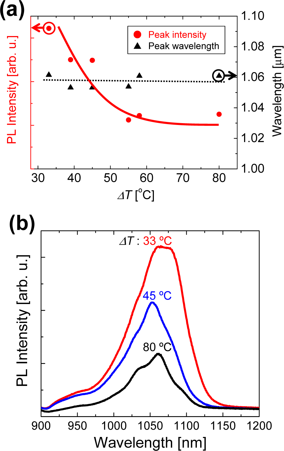
(a) Plots of the PL peak intensity and wavelength as a function of ΔT. (b) PL spectra of the In-flushed QDs for different ΔT. (Reprinted with permission of Ref. 58, Hino Y, et al., J. Cryst. Growth 378, 501 (2013). Copyright Elsevier).
These results demonstrate that the emission intensity and bandwidth of the In-flushed QDs can be controlled by optimizing ΔT in the In-flush process, and the peak wavelength can be maintained at 1.05 μm. The increase in the emission intensity corresponding to a decrease in ΔT can be attributed to suppression of the introduction of non-radiative centers at the interface of the QD and the surrounding GaAs layer. Furthermore, the larger bandwidth is due to the height distribution of the QDs being maintained with a lower ΔT.
We conclude that In-flushed QDs with higher emission intensities and larger bandwidths can be obtained by reducing the value of ΔT. It is possible that a ΔT value less than 33 °C will enable a further increase in the intensity and bandwidth. However, the peak wavelength would also increase. Consequently, optimization of ΔT is essential in the In-flush process to obtain a high emission intensity while maintaining the desired emission wavelength.
4.3 Stacked In-flushed InAs/GaAs QDs
Based on the results above, we fabricated samples including multiple-stacked In-flushed QD layers to obtain a broadband and dip-less emission spectrum centered at around 1.05 μm by controlling the emission center wavelength and intensity of each QD layer [59]. As shown in Figure 22, we first utilized three kinds of In-flushed QD layers, with wavelengths controlled by dcap (1.4, 2.0 and 2.4 nm). The In-flushed QDs were grown between 30-nm thick GaAs spacer layers after the growth of a GaAs buffer layer approximately 300 nm in thickness. In addition, 10-nm thick Al0.3Ga0.7As barrier layers were grown below and above the QD layers to confine the charge carriers. We optimized the annealing temperature (ΔT) in the In-flush process for each QD layer, in accordance with the previous results, to prevent a reduction in the emission intensities. The optimized ΔT value was varied between 32 and 60 °C depending on the dcap value of the QD layer with the intention of equalizing the PL intensities of the QD layers.

(a) Schematic profile and TEM image of the sample including stacked In-flushed QDs with different dcap values (=1.4, 2.0, 2.4 nm). (b) Typical PL spectra of the In-flushed QDs for each dcap. (Reprinted with permission of Ref. 59, Ozaki N, et al., Phys. Status Solidi C 10, 1361 (2013). Copyright Wiley-VCH.).
Figure 23 shows an RT-PL spectrum obtained from a sample of three stacked In-flushed QD layers. A Gaussian-like emission spectrum was observed over a wavelength range of approximately 0.9–1.2 μm as expected from the emission spectra obtained individually from each In-flushed QD layer. The emission peak wavelength was approximately 1.09 μm, and the bandwidth was approximately 92 nm. In comparison with the bandwidth of each In-flushed QD layer grown under the same conditions (shown in Figure 22), an increase in the bandwidth of more than 40 nm was obtained. This broadening can be attributed to a summation of the emission intensities of the stacked QD layers.
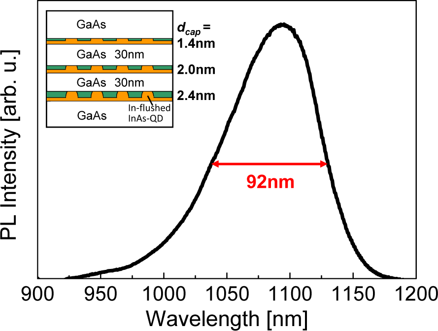
PL spectrum obtained from three stacked layers of In-flushed QDs with different dcap and ΔT. (Reprinted with permission of Ref. 59, Ozaki N, et al, Phys. Status Solidi C 10, 1361 (2013). Copyright Wiley-VCH).
If this spectrum is used as a light source for OCT, then the axial resolution in the OCT image can be estimated to be roughly 5.7 μm from 0.44λ02/Δλ. In addition, the shape of the obtained spectrum is smooth without any dips and is close to Gaussian. This feature is also effective for reducing noise in OCT images.
However, the spectrum is slightly asymmetric, and the peak wavelength is larger than 1.05 μm. This implies that the emissions from the In-flushed QDs with smaller dcap values are still weak. We therefore grew a sample with more stacked layers of In-flushed QDs to increase the intensity of the spectrum below the peak wavelength of 1.09 μm. As shown in Figure 24, by adding two more In-flushed QD layers (dcap = 2.0 nm), a broader emission spectrum than the three-layer stacked sample was obtained. The emission intensity of the In-flushed QD with thinnest GaAs capping (dcap = 1.4 nm) was still lower than that of the In-flushed QD with medium GaAs capping (dcap = 2.0 nm) even though the ΔT was optimized. Thus, we decided to increase the number of layers of the In-flushed QDs with medium GaAs capping (dcap = 2.0 nm) to increase the bandwidth and tune the peak wavelength of the total PL emission to 1.05 μm.

PL spectrum obtained from five stacked layers of In-flushed QDs. By adding two more In-flushed QD layers (dcap = 2.0 nm), the bandwidth increased to 102 nm. (Reprinted with permission of Ref. 59, Ozaki N, et al, Phys. Status Solidi C 10, 1361 (2013). Copyright Wiley-VCH).
The bandwidth of the spectrum increased to 102 nm. Although a small dip in the intensity appeared, the emission spectrum exhibits intensity at shorter wavelengths compared to that of the three-layer stacked sample as expected by adding more In-flushed-QD layers. According to a precise estimation using the coherence function of the spectrum, an axial resolution of 4.5 μm in air can be achieved using this structure as a light source in an OCT system [59].
The emission spectrum was obtained at an excitation power density of ∼300 W/cm2, and under this comparatively low excitation power, the spectrum is expected to be dominated by GS emissions of the In-flushed QDs. By assuming that a higher excitation power will be provided in a practical SLD device, the emission spectrum of an SLD based on In-flushed QDs is expected to exhibit a broader bandwidth and a smaller center wavelength close to 1.05 μm due to the combined ES emissions of the QDs. Consequently, an axial resolution of less than 4.5μm and a large penetration depth in biological samples can be expected for OCT applications.
5. Current-induced luminescence from multi-color QDs
We have discussed above the emission wavelength controllability of self-assembled QDs with results of PL measurements. Considering those techniques introduced into a practical broadband light source for OCT, a current-induced luminescence (EL) from the wavelength-controlled QDs should also be evaluated. Here, we introduce our preliminary result of EL measurements obtained from QDs with controlled emission wavelengths.
We fabricated a straight RWG including multiple vertically-stacked QD layers. The QDs' emission wavelengths were controlled by thicknesses of SRLs and embedded in a 240-nm thick GaAs active layer with 48-nm thick GaAs spacer layers. The active layer is optically and electronically confined with 1.5-μm thick p-/n-Al0.35Ga0.65As cladding layers. The growth conditions of each QD layer, such as SRL thickness, were identical with the abovementioned QDs grown with the rotational MM, as shown in Figure 6. The edge of the RWG was as-cleaved. The EL emission spectrum from the cleaved edge was measured with an InGaAs array detector attached to a monochromator through an objective lens.
Figure 25 shows EL spectrum at RT obtained from the edge of the RWG with applied voltage of 1.2 V. Emission with a width of ∼140 nm was obtained, and the emission wavelength range was found to be consistent with that of the PL spectra obtained from the QDs grown under the same conditions, as shown in Figure 7(b). Emissions spanning approximately 1150 and 1300 nm mainly originated from the QD GS, and the emissions spanning 1050–1200 nm results from the contributions of ES from QD1–4. The emission appears to spread to shorter wavelengths as compared to the GS emission. This can result from contributions of increased ES emissions from the QDs under higher excitation by current injection than photo-excitation. EL emissions from the QDs and ES emission contributions were confirmed, and we conclude that the QDs can be applied to a practical current-induced light source device, and, in particular, to our proposed spectral-shape-controllable broadband light source based on the integration of monolithically grown multi-color QDs.

EL spectrum obtained at RT from RWG including four stacked, multi-color QDs embedded in a p/n-junction
6. Summary and Outlook
We have presented here a review of the developments in broadband NIR light sources based on InAs-QDs. We outlined our proposed spectral-shape-controllable light source based on monolithically grown multiple QDs, and the growth techniques that have been developed for controlling the growth area and emission wavelength of the self-assembled InAs QDs on GaAs substrate. By using a rotational MM, multi-color QDs can be monolithically grown on GaAs substrate, and with the use of RWG, a combined PL emission of the QDs with a linewidth of 160 nm is obtained. Control of the spectral shape has been demonstrated by varying the excitation power for each QD ensemble. Furthermore, we showed that wavelength control methods are compatible with SAG. Bi-layer QD structures are useful for extending the emission wavelength to approximately 1.4 μm, and In-flushed QDs provide an alternative approach to emission wavelength adjustment for light sources with a center wavelength of 1.05 μm. We have been able to obtain wavelength control over a range of 0.9–1.4 μm for InAs QDs grown on GaAs substrate. This implies that there is a possibility of obtaining an ultrabroadband NIR light source with a bandwidth of over 500 nm. Furthermore, we confirmed electrically driven light emission from multi-color QDs with SRLs by embedding the QDs in a conventional p/n-junction configuration. As a next step, we are developing an electrically driven and spectral-shape-controllable light source by utilizing segmented electrodes [60] for each QD ensemble. We expect to be able to control the gain and spontaneous emission of each element in a similar manner to that demonstrated here through PL.
Footnotes
7. Acknowledgements
This study was partly supported by Grants-in-Aid for Scientific Research (KAKENHI) (Grant Numbers 22560016, 23760015 and 25286052), the Canon Foundation, the CASIO Science Promotion Foundation, the Nippon Sheet Glass Foundation for Materials Science and Engineering, the Yazaki Memorial Foundation for Science and Technology, the A-STEP from Japan Science and Technology Agency (JST), Research Support Project of Wakayama University, and EPSRC Grant EP/I018328/1. RWG fabrication was supported by the NIMS Nanofabrication Platform of the “Nanotechnology Platform Project” sponsored by the Ministry of Education, Culture, Sports, Science and Technology (MEXT) of Japan. TEM observations were supported by the Inter-university Cooperative Research Program of the Institute for Materials Research, Tohoku University.