
Abstract
Introduction:
A one-dimensional ZnO nanostructure is a versatile and multifunctional n-type semiconductor. In this paper, ZnO nanorods were successfully prepared by the anodic arc plasma method in an oxidizing atmosphere.
Methods:
The composition, morphology, crystal microstructure, and optical properties of ZnO nanorods were characterized by using X-ray diffraction (XRD), high-resolution transmission electron microscopy (HRTEM) and the corresponding selected-area electron diffraction (SAED), X-ray energy dispersive spectrometry (XEDS), ultraviolet-visible (UV-VIS) spectroscopy, Raman scattering spectrum (Raman), and photoluminescence spectrum (PL).
Results:
The experiment results show that ZnO nanorods synthesized by this method possess hexagonal wurtzite crystal structure with good crystallization, no other impurity phases are observed, the crystalline size is about 18 nm, and the lattice constant distortion occurs compared to that of bulk ZnO. The morphology of the sample is a rod-like shape, the length ranges from 100 nm to 300 nm, the average diameter is approximately 20 nm, and the aspect ratio is relatively high. The UV-VIS absorption spectrum occurs red shift, The Raman spectrum further demonstrates that the major peaks are assigned to ZnO optical vibrational modes, and the PL spectrum exhibits coexistence properties of ultraviolet (UV) and green emission.
Conclusions:
The results prove that ZnO nanorods with hexagonal wurtzite crystal structure were successfully prepared by the anodic arc plasma method in an oxidizing atmosphere.
Introduction
One-dimensional nanostructures display novel properties that significantly differ from those of a corresponding bulk solid state owing to the small size effect, surface effect, quantum size effect, and macroscopic quantum tunnel effect. 1 ZnO is a versatile and multifunctional n-type direct semiconductor with wide band gap energy (3.37 eV) and large exciton binding energy (60 meV).2, 3 In recent years, One-dimensional ZnO nanostructures have attracted considerable attention due to their unique physical, optical, and electric properties,4–6 which have a broad application prospect in different areas such as ultraviolet absorbers, photodetectors, light-emitting diodes, solar cells, spin field-effect transistors, field-emission devices, gas sensors, non-volatile memory devices, and quantum computers,7–13 etc. However, the property and application of one-dimensional ZnO nanostructures are greatly affected by the particle size, morphology, composition, and dimensionality. 14 Therefore, it is urgently important to control the properties of ZnO nanostructures during the synthesis process.
Various methods have been used to fabricate one-dimensional ZnO nanostructures, such as hydrothermal synthesis, 15 thermal evaporation, 16 template-assisted method, 17 chemical vapor deposition, 18 and metal organic chemical vapor deposition, 19 etc. Among these synthesis methods, the plasma method is the most efficient to synthesize various nanostructures due to its many advantages: 20 nanostructures prepared by this method have uniform size, higher purity, narrow size distribution, and are well dispersed. Furthermore, the physical and chemical properties can be easily controlled by adjusting the processing parameters without tedious procedures or special equipment. In addition, this method possesses the potential for further industrialization production with high yield and low cost.
In this paper, we report a simple route to prepare ZnO nanorods by the anodic arc plasma technique. The composition, morphology, crystal microstructure, and optical properties of the sample were examined by using X-ray diffraction (XRD), high-resolution transmission electron microscopy (HRTEM) and the corresponding selected-area electron diffraction (SAED), X-ray energy dispersive spectrometry (XEDS), ultraviolet-visible (UV-VIS) spectroscopy, Raman scattering spectrum (Raman), and photoluminescence spectrum (PL).
Methods
Materials synthesis
The detailed experimental apparatus are fully illustrated elsewhere. 21 These mainly include the stainless steel vacuum chamber, the gas supply device, the DC power supply, the plasma generator with a high frequency initiator, the vacuum pump, the water-cooled collection cylinder, and the water-cooled copper crucible. The bulk zinc served as the anode laid on the water-cooled copper crucible, and the graphite rod served as the cathode. In the process of preparation, the vacuum chamber was pumped to 10-3 Pa and then a mixture of O2 and Ar (1:4 by volume ratio) were backfilled as a reactant gas to reach the desired pressure. The electric arc in the inert environment was automatically ignited between the graphite electrode and the crucible by the high frequency initiator, which was maintained by the current source at the pre-established values of the voltage and current. The bulk raw materials were heated by the high temperature of the plasma, and then evaporated to gasify. When the vapor concentrations exceed saturation, ZnO nuclei spontaneously and homogeneously nucleated in the aerosol systems. ZnO embryos were rapidly cooled and combined to form ZnO nanorods by an aggregation growth mechanism. The products were transported to the inner walls of the cylinder from the nucleation and growth region by means of the free inert gas convection between the hot evaporation source and the cooled collection cylinder. The dispersed ZnO nanorods were collected at the inner walls of the collection cylinder after a period of stabilization with working gas.
Characterization
The phase and crystal structure of the products were determined by X-ray powder diffraction (Japan Rigaku D/Max-2400) equipped with a monochromatic high-intensity CuKa radiation (λ = 1.54056 Å, 40 kV, 100 mA). The products were scanned in the range from 20 to 80° (2θ) with scanning rate 0.005°/s and step size 0.02°. The morphology and the corresponding SAED of the samples were examined by JEM-2010 HRTEM. The chemical compositions of the products were verified by XEDS at an acceleration voltage of 200 keV. The UV-VIS absorption spectrum of samples was recorded by an ultraviolet-visible (Purkinje UV-VIS, TU-1901) spectrophotometer. The measurement of the Raman spectrum at room temperature in the energy region between 100 and 1500 cm−1 were observed by using a micro Raman spectrometer (HR800) with 525 nm line of He-Ne ion laser as exciting light source. The photoluminescence (PL) spectrum of the products was performed at 325 nm wavelength using a Perkin Elmer spectrophotometer of a He-Cd laser with an output power of about 2 mW as the excitation source.
Results and discussion
Structural analysis
Figure 1 shows the XRD patterns of ZnO nanorods, it is obvious that all the diffraction peaks are low and broad due to the small size effect and incomplete inner structure of the particles. The diffraction peaks centering around 2θ = 31.76°, 34.44°, 36.42°, 47.58°, 56.64°, 62.9°, 66.5°, 68.02°, and 69.1° can be perfectly assigned to reflections of (100), (002), (101), (102), (110), (103), (200), (112), and (201) crystallographic planes, respectively, which well indexed with the single-phase hexagonal wurtzite ZnO structure. The peak position and relative intensity of the characteristic peaks readily match with the standard spectrum (JCPDS 36-1451). In addition, no extra diffraction peaks assigned to other impurity phases are detected from the XRD pattern, and the diffraction peaks intensity of (101) crystal planes is the most intense, which indicates that the ZnO nanorods grow along the (101) direction.
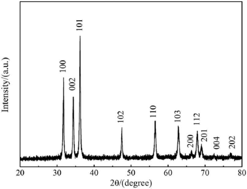
XRD pattern of ZnO nanorods.
Based on the XRD results, the average crystalline size of the products is estimated from the full width at half maximum (FWHM) of the corresponding most intense diffraction peaks (101), according to the Debye–Scherrer equation, as follows:
where D represents the average crystalline size, K = 0.89 is the Scherrer constant, λ is X-ray wavelength (CuKa, 1.54056 Å), θ is the Bragg’s diffraction angle, and B is the broadening of the diffraction line measured at half of its maximum intensity in radian. The crystallite size of the sample is about 18 nm. XRD peaks broadening may also be caused by lattice distortion. The contributions of the crystallite size and lattice strain to diffraction peak broadening can be calculated by the Williamson–Hall (W-H) plots equation 22
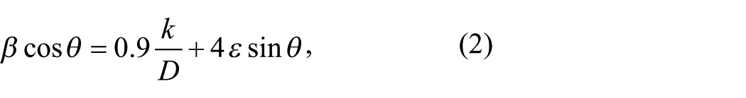
where β is the measured FWHM of XRD corresponding to different crystal planes, θ is the Bragg angle, ε is the effective strain, and D is the crystallite size. The Williamson–Hall plot (βcosθ vs 4sinθ) for the ZnO sample is shown in Figure 2. Based on the linear fitting to the experimental data, the crystalline size is estimated from the y-intercept, and the strain ε from the slope of the fitted line. The effective crystallite size and lattice strains for the ZnO sample is 22 nm and 0.004, respectively. The crystallite size estimated from both the methods (Debye–Scherrer and Williamson–Hall) is in good agreement.
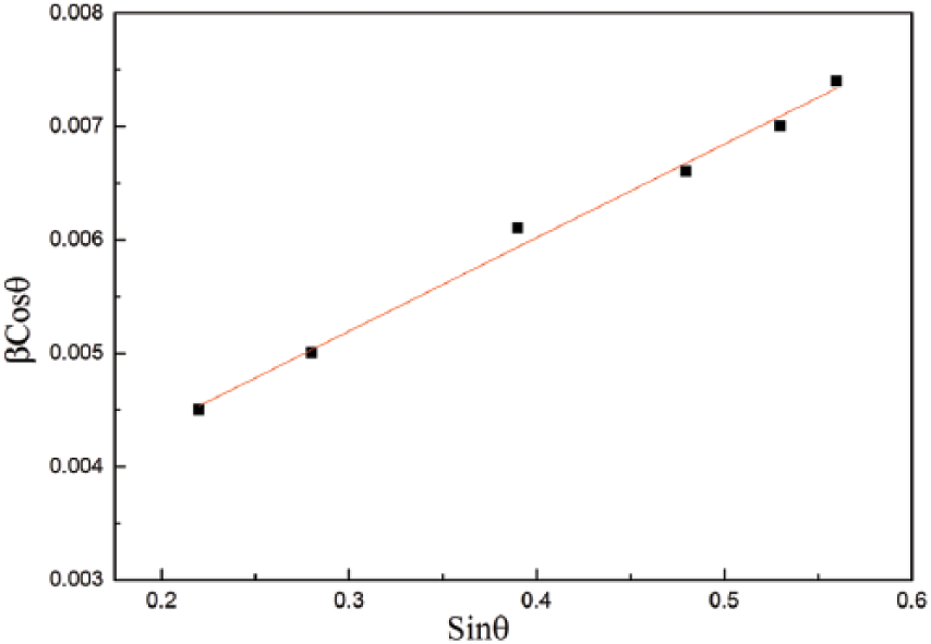
Williamson–Hall plot of ZnO nanorods.
The microstructure data of ZnO nanocrystals are calculated according to the Bragg formula

and the crystallographic formula
where dhkl denotes the crystalline plane distance, hkl is indices of crystal face, and θ is the diffraction angle of the (101) peak. The lattice constant a is obtained for the (100) plane through the relation
and the lattice constant c is derived for the (002) plane using the relation
respectively. For ZnO nanocrystals, the crystalline plane distance dhkl of (101) Miller plane is about 2.458 Å; the values of the lattice parameters a and c are 3.24 Å and 5.20 Å, respectively, which are slightly larger than that of bulk ZnO (a = 3.2352 Å, c = 5.1910 Å), and thus cause the lattice distortion.
Morphological studies
In order to explore the surface morphology and microstructure of the obtained samples, the ZnO samples were observed by HRTEM. The representative HRTEM images of the ZnO samples are shown in Figure 3. Figure 3(a) shows that the sample possesses one-dimensional rod-like shapes with clear edge and smooth surface, well dispersed and good length to diameter ratio. The average diameter of the sample is about 20 nm, the length ranges from 100 nm to 300 nm, and the aspect ratio (the ratio of the length to the diameter) of the nanowires is relatively high.
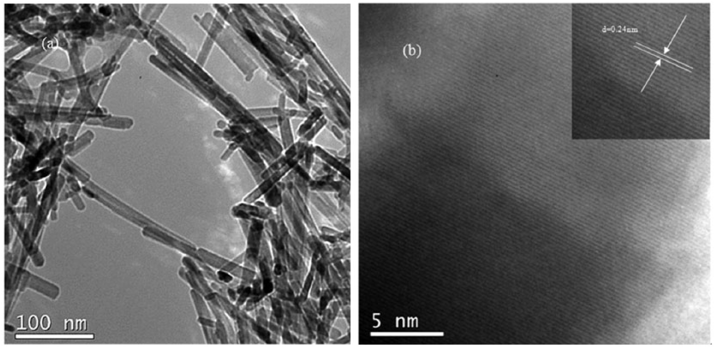
HRTEM micrograph of ZnO nanorods.
Figure 3(b) displays the local high magnification HRTEM micrographs of ZnO nanorods. It can be seen that the ZnO nanorods reveal the clear lattice fringe without stacking faults and dislocations, and well-oriented growth along the (101) direction with good crystallization. It can be estimated from the image of Figure 3(b) that the fringe spacing is approximately 0.25 nm, which is well consistent with the d-spacing of the (101) plane of the hexagonal wurtzite ZnO structure. This further confirms that the samples grow along the (101) direction and this is in accord with the result of XRD.
Figure 4 shows the corresponding SAED pattern of ZnO nanorods, the SAED pattern consists of many regular concentric rings with different radii, which indicates that the samples belong to polycrystalline structure. The diffraction rings from inside to outside can be indexed to (100), (002), (101), (102), (110), (103), and (112) crystal planes of the hexagonal wurtzite ZnO structure, respectively. The SAED pattern further confirms that the sample is a hexagonal wurtzite ZnO structure in crystallography, which is in agreement with the result of XRD.
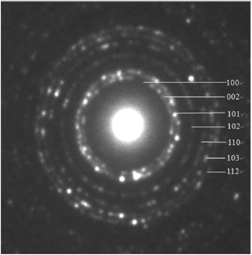
SAED pattern of ZnO nanorods.
Based on the above experimental results, we propose a plausible growth mechanism of ZnO nanorods prepared by the anodic arc plasma method. In the process of preparation, the bulk metal zinc was heated and melted by the high temperature of the plasma, and metal atoms detached from the metal surface when the plasma jet kinetic energy exceeded the metal superficial energy, and it ultimately evaporated into free atom state. Above the evaporation source there was a region of supersaturated metal vapor, where Zn atoms diffused around and collided with O atoms to form ZnO to decrease the nucleus forming energy at high temperature due to the oxidation reaction. When the concentrations of the vapor exceed saturation, ZnO embryos nucleated homogeneously in the aerosol systems. ZnO nuclei were rapidly cooled and combined to form primary clusters by an aggregation growth mechanism. Because of the anisotropy of ZnO crystals, the growth velocities of the ZnO crystals in different directions were different. In other words, the growth of ZnO crystals were dependent upon the growth velocity of the different planes. The growth velocity of plane (101) direction was the fastest compared to other growth facets, therefore the (101) direction was the dominant growth direction, and ZnO nanorods finally formed.
Composition analysis
In order to further clarify the chemical compositions of the as-prepared samples, an XEDS measurement was performed. The XEDS spectrum of the ZnO samples is given in Figure 5. It is easily found that the as-prepared samples mainly contain Zn and O elements characteristic peaks. The characteristic peaks of O appeared at 0.5 keV, and the characteristic peaks of Zn appeared at 1.8 and 8.9 keV, further confirming the chemical formation of ZnO. Besides these, the Cu and C peaks in the XEDS originate from the TEM micromesh grid of the bearing samples during the testing process, and the characteristic peaks of Cu appeared at 0.9, 8 and 8.9 keV. The XEDS results further verify the XRD conclusion, which indicates that ZnO nanorods were successful synthesized by the anodic arc plasma technique.
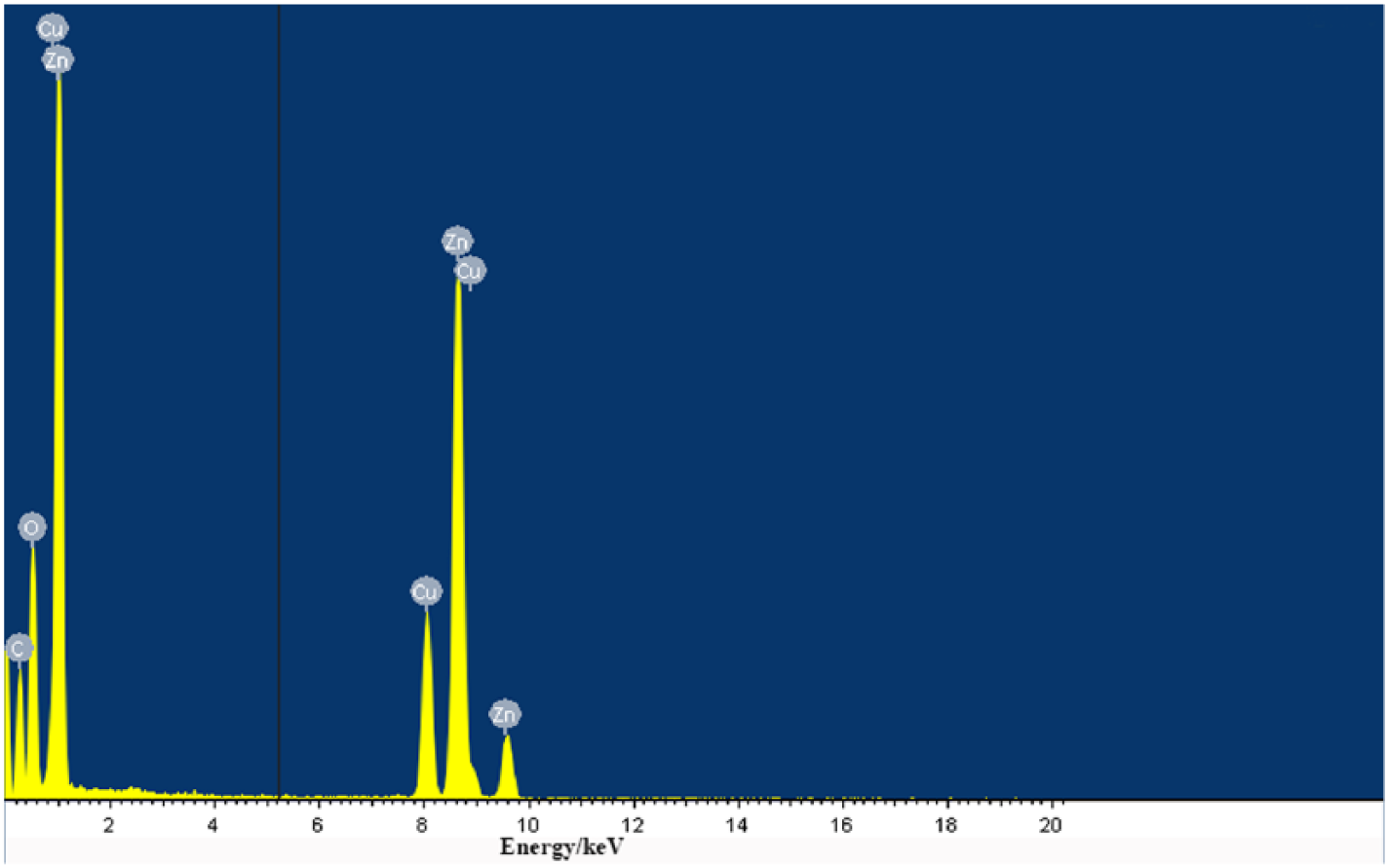
XEDS spectrum of ZnO nanorods.
Optical properties
Figure 6(a) shows the room-temperature UV-VIS absorption spectrum of ZnO nanorods. It is clear that the sample exhibits a broad and strong absorption edges band at UV region in the range of 280–380 nm and poor absorption at visible region. Based on the UV-VIS results, the optical band gap can be calculated, according to the Tauc relation, as follows

where hν is the incident photon energy, ν is the photic frequency, Eg is the optical band gap, A=4πk/λ represents the absorption coefficient with k and λ representing the absorbency and wavelength, respectively, and h is the Plank’s constant; α is the absorption coefficient which can be obtained using the Kubelka–Munk function
where R is the percentage of reflected light. For a ZnS nanocrystals semiconductor with direct band structure, n = 1/2, and (αhν)2 gives the best linear fitting curve in the band edge region. The relationship between (αhν)2 and hν is shown in Figure 6(b). The values of Eg are obtained by extrapolating the straight portion of the curve on hν axis at α = 0. The measured value of optical band gap energy for ZnO nanorods is 3.27 eV. It is clear that the direct band gap value of the ZnO sample is smaller than that of bulk ZnO (3.37 eV) and occurs as a red shift phenomenon. This may be due to the energy gap becoming narrower with the decrease of the particle size. This may be attributed to the narrower energy gap with the decrease of the particle size, which leads to the optical absorption band shift to the long wave direction. On the other hand, small particle size and large surface tension lead to the lattice distortion and the increase of lattice constants, the distortion inside the particle makes the bond length longer, and the infrared absorption band shifts to lower wave number, therefore the interface effect causes the spectral red shift of nano materials.
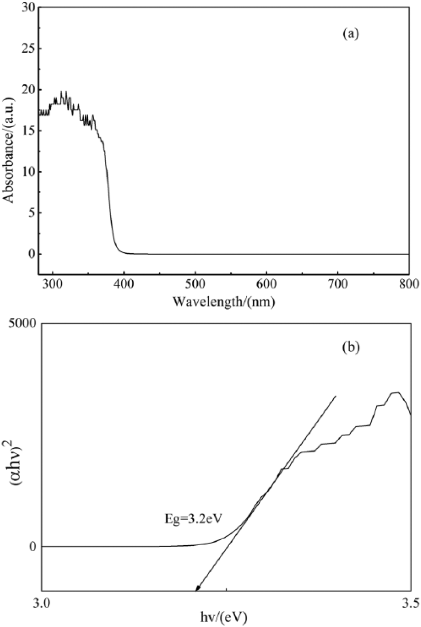
(a) Absorption spectrum of ZnO sample, and (b) Tauc plot of (αhν)2 versus of ZnO nanorods.
Wurtzite structure ZnO as an n-type semiconductor with the space group 63mc possesses Brillouin zone center optical phonon modes 23 :

where the A1 and E1 modes exhibit Raman and infrared activity, but the E2 model only has Raman activity, B1 has neither Raman activity nor infrared activity, and A1 and E1 models are polar and split into the transverse optical (TO) and longitudinal optical (LO) phonons. The E2 mode consists of E2 high and E2 low modes. E2 high is associated with the vibration of oxygen atoms, and E2 low attributes to the Zn sub lattices. E1 vibration is related to the defects such as oxygen vacancies, Zn interstitial or their compound, and E2 vibration is related to the stress in crystals. Figure 7 shows the Raman spectrum of ZnO nanorods was measured with an excitation wavelength of 532 nm at room temperature. The spectrum of ZnO nanorods exhibits three prominent peaks at 322, 428, and 532 cm−1. The peak at 330 cm−1 is attributed to the second order Raman mode arising from zone boundary phonons E2 high and E2 low modes, and the characteristic peak at 428 cm−1 belongs to E2 high mode, which indicates that the sample possesses a hexagonal wurtzite crystal structure. Moreover, the broad band centering at 574 cm−1 belongs to the coupling of A1(LO) and E1(LO) vibration modes. This result proves that the lattice vibration of ZnO nanorods exhibits multi phonon characteristics by comparing with those of the bulk one.
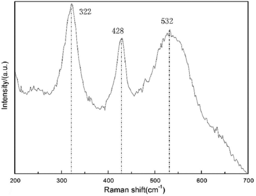
Raman patterns of ZnO nanorods.
Figure 8 presents the room-temperature PL spectrum of the ZnO nanorods. The spectrum mainly consists of two main emission peaks centering at 395nm and 545 nm, respectively. The broad and intense emission band at 393 nm (3.14 eV) is corresponding to the near-band-edge (NBE) emission of wide band gap of ZnO as a result of the excitonic recombination due to the quantum confinement effect. The strong green emission band centering at 545 nm (2.28 eV) is possibly assigned to positively charged electron transition and surface traps mediated by defects in the band gap, or attributed to the recombination of electrons in singly occupied oxygen vacancies with photo-excited holes in the valence band. The strong intensity of UV emission and green emission should be attributed to the high purity with good crystallinity of the synthesized ZnO nanorods, which is consistent with Raman spectroscopy.
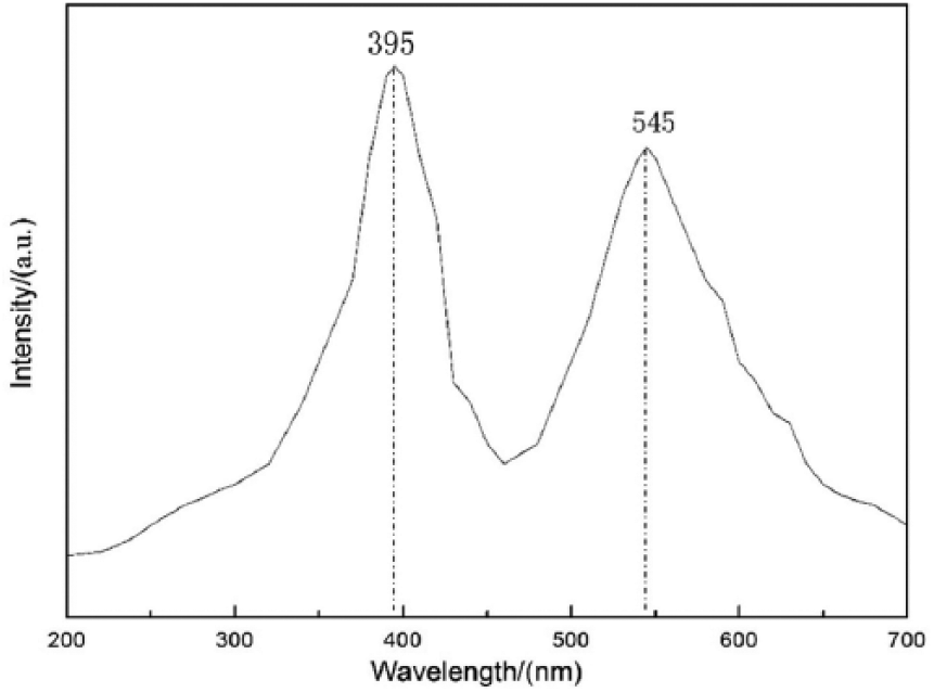
PL spectrum of ZnO nanorods.
Conclusions
(1) ZnO nanorods were successfully prepared by the anodic arc plasma method, the samples possess hexagonal wurtzite crystal structure with good crystallization, the crystalline size is about 18 nm, and the lattice constant distortion occur compared to that of bulk ZnO.
(2) The morphology of the sample is a rod-like shape with smooth surface and clear edge, the length ranges from 100 nm to 300 nm, the average diameter is approximately 20 nm, and the aspect ratio is relatively high.
(3) The UV-VIS absorption spectrum indicates the energy band gap decreases and occurs red shift compared to that of the bulk ZnO. Raman spectrum further demonstrates that the major peaks are assigned to ZnO optical vibrational modes. PL spectrum exhibits coexistence properties of ultraviolet (UV) and green emission.
Footnotes
Declaration of Conflicting Interests
The author(s) declared no potential conflicts of interest with respect to the research, authorship, and/or publication of this article.
Funding
The author(s) disclosed receipt of the following financial support for the research, authorship, and/or publication of this article: Financial support: this work was financially supported by the National Natural Science Foundation of China (grant number 51261015) and the Natural Science Foundation of Gansu Province, China (grant number 1308RJZA238).