
Abstract
The integration of nanomaterials in microfluidic devices has emerged as a new research paradigm. Microfluidic devices composed of ZnO nanowires have been developed for the collection of urine extracellular vesicles (EVs) at high efficiency and in situ extraction of various microRNAs (miRNAs). The devices can be used for diagnosing various diseases, including kidney diseases and cancers. A major research need for developing micro total analysis systems is to enhance extraction efficiency. This article presents a novel fabrication method for a herringbone-patterned microfluidic device anchored with ZnO nanowire arrays. The substrates with herringbone patterns were created by maskless photolithography. The ZnO nanowire arrays were grown on the substrates by chemical bathing. The patterned design was to introduce turbulent flows as opposed to laminar flow in traditional devices to increase the mixing and contact of the urine sample with ZnO nanowires. The device showed reduced flow rates compared with conventional planar microfluidic channels and successfully extracted urine EV-encapsulated miRNAs.
Introduction
Development of microfabrication technologies has enabled many novel and exciting engineering prospects, especially the concept of lab-on-a-chip (micro total analysis systems). This allows medical professionals to execute complex diagnostic tests with increased efficiency. Microfluidics, a field dealing with fluid flow inside a micro-scale channel, allows for the manipulation of small volumes of liquids and gives the ability to perform various liquid analyses with small samples in an effective manner, including sample pretreatment, reaction, separation, and detection. 1 The research on microfluidic devices has increased exponentially over the years and has shown great promise in a varied array of biomedical applications, such as cell sorting,2,3 enzymatic arrays, 4 polymerized chain reaction (PCR), 5 and so on. The main advantages in microfluidics reveal increased efficiency, high throughput, and disposability using small sample size and low production cost per device when compared with other techniques; faster sampling times with conduction of parallel processing of samples; accurate, precise control of multiple samples and reagents simultaneously; and increased sensitivity with versatile formats for the incorporation of various detection schemes. 6
Integration of nanomaterials in microfluidic devices has emerged as a new research paradigm. Nanowires are defined as structures with no length constraint, but with diameter limited to 10–9 m or less. However, in general, nanowires have a length-to-width ratio of greater than or equal to 1000. 7 Zinc oxide (ZnO) nanowires possess very unique properties due to their semiconducting nature and are used in a wide array of applications: biological and biomedical applications, corrosion protection, semiconductor devices, optical coating, manufacturing of nanodevices, solar cells, gas sensor, and so on. 8 Due to its low toxicity and biodegradability, ZnO is vastly used in the field of biomedicine such as the delivery of drugs and genes, biosensors and bioimaging which consists of magnetic resonance, fluorescence, positron emission tomography, and dual-modality imaging. 9 In addition, ZnO nanowires coated with hydrophobic surfaces are used for medical tools and surgical equipment. 10 Yasui et al 11 developed a microfluidic device composed of nanowires which enable the collection of urine extracellular vesicles (EVs) at high efficiency and in situ extraction of various microRNAs (miRNAs) of different sequences. miRNAs are small non-coding RNA molecules that are associated with post-transcriptional regulation of gene expression. 12 Recent studies have successfully tied changes in miRNA found inside EVs to different pathophysiological conditions. 13 Valadi et al 14 demonstrated that exomes contain both mRNA and miRNA. These can be successfully sequestered from various body fluids, including plasma, malignant ascites, urine, amniotic fluid, breast milk, and saliva, and serve as a biomarker for disease. 15 Over the years, various research groups have demonstrated that miRNA profiling could be used as diagnostic markers for biopsy profiling, 16 differentiating between hepatocyte injury and inflammation, 17 diagnosing the grade and stage of liver diseases. 18 In addition, exosomes are known to secrete into the urine from all nephron segments. 19 Consequently, urinary exosomes will contain miRNAs that will be associated with various kidney diseases. 20 Furthermore, ZnO nanowire-anchored microfluidic devices could potentially serve as biomarkers for cancers and other diseases.
The concentration of EVs in urine is less than 0.01% of the volume. Therefore, collecting and analyzing mRNAs from clinical urine samples still remains a challenge. 21 Conventional methods like ultracentrifugation have allowed to successfully extract and identify about 200-300 urinary miRNAs. 21 However, this is an extremely low number compared with more than 2000 miRNAs that are present in the human body. It is of great importance to enhance the extraction efficiency for micro total analysis systems and lab-on-a-chip systems.
It is widely believed that efficient mixing schemes are critical for increasing the throughput of miRNA extraction. 22 Traditional microfluidic devices rely on diffusion in mixing processes. 23 Moreover, in traditional devices, flow has a low Reynolds number for creating a laminar flow. Thus, researchers can rely on diffusive mixing by bringing multiple streams together. 24 But this approach is very time-consuming and requires a sufficient channel length. 24 For this reason, creating proper and efficient mixing inside a microfluidic channel has attracted much attention over the years. Current methods include active mixers such as mechanical stirring, 25 magneto-hydrodynamic stirring,26,27 electro-hydrodynamic stirring, and acoustic streaming. 28 In all cases, active mixers require complex fabrication designs and external power sources. As an alternative, Johnson et al 23 showed that microfluidic channels with anisotropically patterned groves could create a turbulent flow and increase the mixing efficiency over a shorter channel length. Studies have also shown that staggering herringbone grooves with proper designs resulted in higher mixing in microfluidic systems. 29 The main challenge of fabricating microfluidic devices with topological features is the complexity and high cost of traditional lithography. There is a research need for facile fabrication of microfluidic systems integrated with nanomaterials and nanostructures.
In this article, we propose a ZnO nanowire-anchored microfluidic device fabricated via maskless photolithography for extracting urine EV-encapsulated miRNAs. This novel fabrication method offers an easy-to-operate and low-cost alternative to existing methodologies.
Materials and Methods
Pattern design
The microfluidic device was divided into 2 parts. We used an open source software Klayout 0.25.8 to design the top and the base of the device. As shown in Figure 1, the bottom part was a herringbone structure. The width of both the structure and the gap was set to be 500 µm. The angle between the structure and the axis was 45°. The total length and breadth were 40 and 4 mm, respectively.

K-Lay out images of the (A) bottom part with a herringbone structure, and (B) top part with 2 reservoirs.
The top part was a straight channel with 2 circular reservoirs at the ends. The geometry was 39.5 mm in length and 3.5 mm in breadth, and 10 mm in the reservoir diameter.
Maskless photolithography
After cleaning the silicon dioxide (SiO2) wafer (University Wafer, South Boston, MA) with acetone, a thin layer of negative photoresist (H.A.R.E SQ10, KemLab, Woburn, MA) was spin-coated by the KW-4A spin coater (SETCAS LLC, San Diego, CA). Two milliliters of the negative resist were placed in the middle of the wafer and spun at 500 r/min for 10 seconds and at 1000 r/min for 60 seconds. Using the focal length function on the Microwriter, we estimated the resist thickness to be 60 µm. The supplier protocol recommends a 2-step postbaking process with a soft bake at 65°C and a hard bake at 115°C. However, when followed, we noticed thermal stress–induced shrinkage on the resist. To achieve optimum results, we baked the wafer for 15 minutes at 75°C.
As opposed to conventional mask–assisted lithography process, we used maskless direct-write lithography to etch the pattern into silicon oxide wafer via Microwriter ML3 (Durham Magneto-Optics Ltd, UK). The device uses computer-controlled optics to project the exposure pattern directly onto the photoresist (Figure 3). In photolithography, the dosage and intensity of the UV exposure determine the degree of crosslinking and ultimately the photoresist solubility in the developer. Excessive light may result in overexposed areas while a lighter luminous may result in limited penetration into the resist. Hence, series of exposures is recommended for optimal results. 30 Through preliminary tests, we determined that a series of incrementing exposures would result in optimal patterns. The photoresist on the SiO2 wafer was subjected to 4 repetitive exposures with intensities of 250, 500, 750, and 1000 mJ/mm2. Once exposed, we once again baked the wafer at 75°C for 15 minutes. Next, we placed the silicon oxide wafer into the High Aspect Ratio Epoxy Superior Quality (H.A.R.E SQ, Kem Labs, and USA) developer, disturbed the solution for 1 minute, developed the pattern, and then cleaned it with isopropyl alcohol and deionized (DI) water.
For the bottom part, we first coated the SiO2 wafer with ZnO nanowires through a self-assembly process, and then applied the polydimethylsiloxane (PDMS, SYLGARD 184 Elastomer, DOW Corning Co, Midland, MI) on the top of the wafer. After the PDMS was cured, we removed it from the wafer with embedded ZnO nanowires and further grew the ZnO nanowires on the PDMS. The protruded heads of embedded ZnO nanowires served as seeds to initiate the nucleation of ZnO nanowires. 11 The detailed protocol is shown in Figures 2 and 3. To grow ZnO nanowires, we mixed 15 mM (210 mg) of hexamethylenetetramine (C6H12N4, Sigma Aldrich, St. Louis, MO) and 15 mM (446.2 mg) of zinc nitrate hexahydrate (Zn(NO3)2 6H2O, Sigma Aldrich, St. Louis, MO) with 100 mL of DI water and immersed the wafer at 95°C for 3 hours. After 3 hours, the nanowire-grown wafer was cleaned by DI water to rid off any deposited residue and allowed to air dry overnight. To minimize the deposition of any residue, the wafer was suspended upside down in the solution. Then, the PDMS was poured onto the substrate and cured for 6 hours at 65°C. After the PDMS was carefully peeled off from the substrate, the nanowires were transferred to the PDMS from the substrate. The nanowires were deeply buried into PDMS with their heads slightly emerged, and these heads provided growth points for the next step. Nanowires were grown on the PDMS layer through the chemical method explained above.

Direct-write lithography.

Procedures of fabricating the ZnO nanowire-anchored PDMS microfluidic device with herringbone.
For the top part, the PDMS was distributed on the SiO2 wafer and cured. Both the top and bottom parts were cleaned using DI water and allowed to air dry overnight. The PDMS substrates were carefully cut into rectangle pieces and observed under the scanning electron microscope (SEM). The top and bottom pieces were assembled through plasma bonding. A thin layer of PDMS was applied to seal the assembled device and baked at 75°C for 15 minutes. Then, the device was mounted onto a glass slide. Two inlet and outlet holes were drilled into the middle of the circular section, and we attached 2 microtubes, in which 1 of them was connected to a syringe to pump the fluid through.
Flow analysis
Two devices, a patternless microfluidic device and our novel patterned ZnO nanowire-anchored microfluidic device, were connected to a microfluidic control system (Eleveflow OB1 MK3 @ 2019 Elveflow). The flow rate was then recorded at different pressure values and compared. At each pressure value, the fluid was allowed to flow for 1 minute for pressure and flow rate to stabilize before recording the data.
In situ extraction of urine EV-encapsulated miRNAs
Commercially available single-donor urine was used for EV capture and miRNA extraction. The sample was centrifuged for 15 minutes at 4°C, 3000g to remove debris. Then, 1 mL of the sample was pumped into the ZnO nanowire-anchored patterned microfluidic device at a flow rate of 50 μL/min. To extract the miRNA from trapped EVs, cell lysis buffer M (20 mM tris-HCl (pH, 7.4), 200 mM sodium chloride, 2.5 mM magnesium chloride, and 0.05 w/v% NP-40 substitute) was pumped through the device at a flow rate of 50 μL/min.
Results
The developed top part with herringbone patterns on the SiO2 wafer is shown in Figure 4A and B. The structure of the patterns was well developed and clearly defined. Figure 5A to D shows the ZnO nanowires (white substances) grown on the surface. It should be noted that the ZnO nanowires were indiscriminately grown on both SiO2 surface and photoresist surface. The crosslinked photoresist layer did not limit the growth of ZnO nanowires. Cheng et al 31 suggested a method of fabricating high-quality ZnO nanowire arrays directly by photoresists via carbonizing the resist. We conjectured that the postbaking procedure might create nucleation sites for nanowire growth.

(A) SiO2 wafer with etched herringboned design (scale bar at 1 cm). (B) Optical microscope image of the etched pattern (scale bar at 400 µm).

(A-B) SEM image of the PDMS layer after peeled off from the SiO2 substrate (scale bar = 50 μm). (C-D) SEM image of PDMS substrate after nanowire growth (scale bar = 200 μm).
Figure 5 shows the SEM images of the ZnO nanowire-anchored PDMS surface. The nanowires were uniformly distributed over the whole surface. Figure 5A and B shows the PDMS peeled from the SiO2 wafer before immersing in the solution of C6H12N4 and Zn(NO3)2. Nanowires were transferred from the SiO2 substrate into the PDMS and were embedded with their heads slightly emerged. Figure 5C and D shows the PDMS after being immersed for 3 hours in the solution. The nanowires grew from the seeds with random orientations. This result supports our hypothesis that embedded nanowire heads serve as the growth points for secondary growth.
Figure 6 shows the energy-dispersive spectroscopy (EDS) on the PDMS surfaces before and after the solution treatment. The elemental mapping results demonstrate the increased presence of Zn after the nanowire growth. The increase in Zn percentage in Figure 6B was due to the secondary growth of ZnO nanowires. This is backed up by the increased nanowire length seen in Figure 6C and D. The presence of Si was due to the residues from the SiO2 wafer.

(A) Elemental mapping for PDMS layer after peeled off from the SiO2 substrate. (B) Elemental mapping for PDMS layer after being immersed on the nanowire growing solution.
SEM characterization showed that the nanowires had a mean diameter of 131 ± 51 nm, confirming the geometry of the ZnO nanowires was relatively uniform.
After the assembly, the embedded patterns were clearly visible as shown in Figure 7A and B. Two microtubes illustrated in Figure 8A served as the inlet and outlet for fluid flow. When pumping DI water through the connected microtubes, we were able to observe a good and constant flow in this microfluidic device.

SEM images of the channel: (A) Top view. (B) Side view (scale bar = 100 µm).
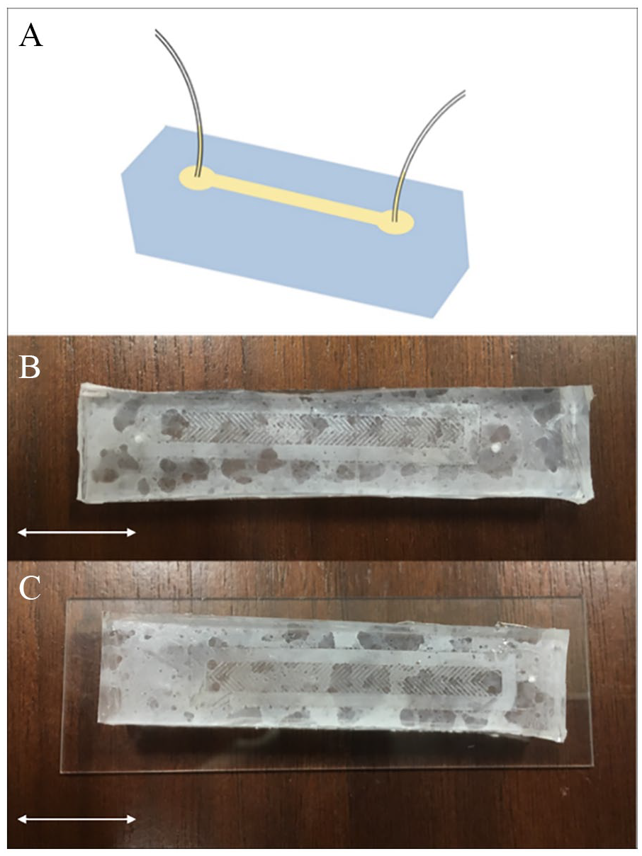
(A) Schematic illustration of the ZnO nanowire-anchored microfluidic device. (B-C) Top view of the final product (scale bar = 20 mm).
Figure 9 represents the flow rate at different pressure values for 2 microfluidic devices with and without pattern. We can observe a decrease in flow rate on our patterned device compared with the patternless device at the same pressure. The flow rates at each pressure level were summarized in Table 1.

Flow rate through the device at different pressure values.
Flow rate through the device at different pressure values.
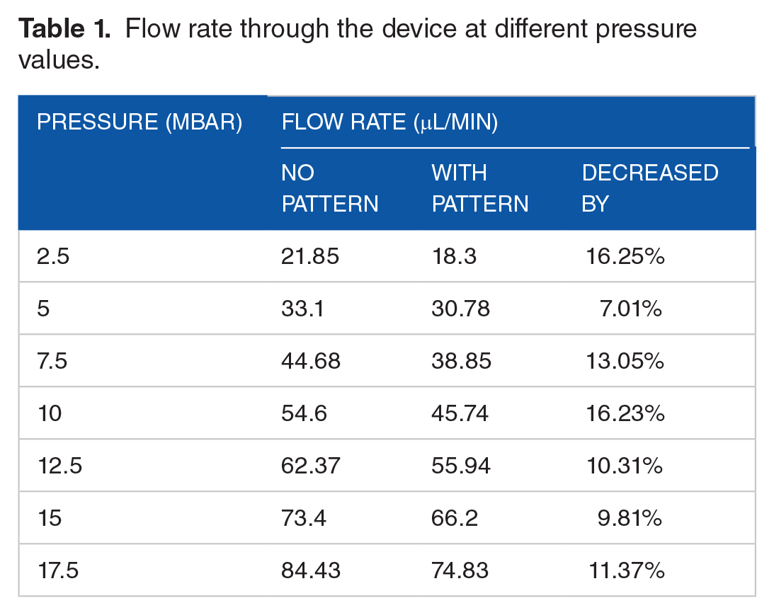
Figure 10A and B represents the transmission electron microscopic images of the extracted fluid. The samples were negatively stained with 2% uryl acetate. Figure 10A represents the extracted microvesicles while Figure 10B shows the protein strands. Both images are similar to other published transmission electron microscope (TEM) images of microvesicles and protein strands.32,33

TEM images of (A) trapped microvesicles (scale bar = 100 nm) and (B) protein strand (scale bar = 500 nm).
Discussion
The growth of ZnO nanowires can be accomplished by various methods. Sadullah Ozturk et al manufactured ZnO nanowires using template-assisted fabrication methods. Anodic aluminum oxide template-assisted cathode induced sol-gel electrodeposition. 34 Noborisaka et al 35 used metal organic vapor phase epitaxy growth technique to manufacture nanowires which were hexagonal and vertical in shape on a substrate made up of gallium arsenide. Lee et al 36 manufactured vertical ZnO nanowires by using chemical vapor deposition technique. In addition, Huang et al 37 adopted the vapor-liquid-solid technique. Yasui et al 11 developed a ZnO nanowire-anchored microfluidic device for EV-encapsulated miRNA analysis. The ZnO nanowire arrays possessed a relatively large surface area with surface charges, which allowed miRNA analysis with a small sample volume (1 mL of urine) and short treatment time (20 minutes). 11 The research group succeeded in extracting a much larger variety of species of miRNAs than ultracentrifugation. In our study, we integrated the ZnO nanowire array and the herringbone structure on the same substrate through a combination of maskless (direct-write) photolithography and chemical bathing method. We will perform the flow analysis and EV extraction to test the hypothesis that this microstructured device will enhance the mixing efficiency and extraction efficiency. In addition, we will study the effects of groove patterns and nanowire orientation randomness on the extraction efficiency.
Our flow test showed that the herringbone pattern reduced the flow rate in the device. Alireza et al conducted a study on the effects of surface corrugations in micro- and nano-channels. In his study, he found that obstacles in the flow path such as a patterned microstructure created a pressure gradient, referred as “form drag,” which caused additional pressure losses. 38 In retrospect, we can expect a reduced flow rate in turbulent flow at the same pressure compared with the laminar flow. Data acquired from the flow analysis showed a decrease in flow rate in the patterned device, suggesting an increased resistance to flow. A numerical investigation carried out by Wang et al on mixing in micro-channels with patterned grooves showed improved mixing efficiency and reduced channel length required for complete mixing. These findings confirmed our initial hypothesis that patterned nanowire-grown microstructured devices will introduce turbulent flow and lower flow rate, and the spiral circulation will enhance the mixing efficiency.
The most widely adopted methods for miRNA extraction nowadays are ultracentrifugation and commercially available kits. Ultracentrifugation technique requires a minimum of 20 mL of urine and a total of more than 5 hours for collection and extraction. 11 Moreover, ultracentrifugation might fuse and rupture most microvesicles due to the forces exerted on them during the process. Commercial kits are faster than ultracentrifugation but still require multistep protocols that include centrifugation, and a total time spanning can be more than 14 hours due to incubation. 39 In comparison with these conventional methods, our proposed device successfully extracted EV-encapsulated miRNAs by introducing 1 mL of urine sample followed by 1 mL of lysis buffer into the device within a total time of 40 minutes. In addition, the proposed device incorporates electrostatic interactions between positively charged nanowires 11 and negatively charged microvesicles. Studies have shown that exosomes and microvesicles will acquire negative charges in a polar medium similar to that of the cell lysis buffer. 40 Therefore, we expect the proposed device to be an easy-to-use, low-cost, fast alternative to EV-encapsulated miRNA extraction. The extraction efficiency of the proposed approach and the level of miRNA expression need to be further studied.
Another important aspect of the device is the ZnO nanowire array. Hydrothermal growth of ZnO nanowires requires strictly controlled conditions. Thus, we will fine-tune the experimental parameters for ZnO nanowire self-assembly to achieve a more homogeneous nanowire forest. In addition, we plan to conduct tests on ZnO nanowire bonding to the PDMS to ensure the mechanical stability of the nanowires during miRNA extraction. We will also perform an in-depth flow analysis and EV extraction test to quantitatively study the relationship between the design features and the mixing and extraction efficiency. Especially, we will study the effects of groove patterns and nanowire orientation randomness on the extraction efficiency.
Conclusions
In this article, we demonstrated a microfabrication method for a ZnO nanowire-anchored microfluidic device integrated with a herringbone surface. The motivation was to introduce turbulent flow that would increase the mixing and extraction efficiency of the EV-encapsulated miRNA from urine samples by ZnO nanowire arrays. Our future research focuses on 2 objectives: first, we will characterize the performance of the device regarding the convection and the diffusion of solutions, studying the effects of microstructural attributes to the flows; second, we will optimize the design and evaluate the EV extraction efficiency from urine samples and develop this system into a diagnostic device for multiple diseases.
Footnotes
Acknowledgements
The authors would like to thank Dr. Hiranmoy Das (School of Pharmacy, Texas Tech Health Sciences Center, Amarillo, Texas) for his assistance with the extraction of urine EVs.
Funding:
The author(s) disclosed receipt of the following financial support for the research, authorship, and/or publication of this article: This work was financially supported by the Foundation of the Whitacre College of Engineering and the Office of Vice President for Research at Texas Tech University.
Declaration of conflicting interests:
The author(s) declared no potential conflicts of interest with respect to the research, authorship, and/or publication of this article.
Author Contributions
DS carried out the pattern design, photolithography, and flow analysis. SM carried out the ZnO nanowire growth. GZT supervised the project. All authors contributed to the final version of the manuscript.