
Abstract
Single-photon emitters in hexagonal boron nitride have attracted great attention over the last few years due to their excellent optoelectronical properties. Despite the vast range of results reported in the literature, studies on substitutional impurities belonging to the 13th and 15th groups have not been reported yet. Here, through theoretical modeling, we provide direct evidence that hexagonal boron nitride can be opportunely modified by introducing impurity atoms such as aluminum or phosphorus that may work as color centers for single-photon emission. By means of density functional theory, we focus on determining the structural stability, induced strain, and charge states of such defects and discuss their electronic properties. Nitrogen substitutions with heteroatoms of group 15 are shown to provide attractive features (e.g. deep defect levels and localized defect states) for single-photon emission. These results may open up new possibilities for employing innovative quantum emitters based on hexagonal boron nitride for emerging applications in nanophotonics and nanoscale sensing devices.
Introduction
The importance of photonic technologies is steadily growing in our daily lives. In the past few decades, developments in light generation and manipulation have allowed for the widespread diffusion of efficient devices, such as lasers and light-emitting diodes. Today, stimulated by the wide field of possible applications, research is focusing on the realization and development of new light sources, able to produce photons whose statistics and correlations are eminently quantum-mechanical. Such nonclassical light sources rely on a fundamental component: the single-photon emitter (SPE). The ideal SPE is an on demand, deterministic source delivering light pulses in a well-defined polarization and spatiotemporal mode and containing exactly one photon. Unlike classical light sources, SPEs are fundamental quantum devices for many scalable and leading technologies, such as quantum information, 1 quantum computing and simulation, 2 precision metrology and imaging, 3 and quantum communication. 4
Up to now, single-photon sources obtained by means of isolated color centers in wide bandgap semiconductors have been realized in a number of systems as three-dimensional (3D) materials, such as diamond 5 –7 and gallium nitride, 7,8 2D materials such as hexagonal boron nitride (h-BN), 9 one-dimensional materials, such as carbon nanotubes 6 and indium phosphide nanowires, 10 and zero-dimensional materials, such as gallium arsenide (GaAs) and indium gallium arsenide quantum dots. 11,12 The ability to tailor and control quantum emitters, to realize efficient and scalable architectures, depends on site-selective defect engineering. To avoid recombination due to thermal effects, defect energy levels need to be deep in the semiconductor bandgap. At the same time, defect states should not present strong hybridization with the host matrix, so that the relative energy levels show little dispersion in reciprocal space and allow for the emission of photons with definite wavelength. 13 Additionally, without taking into account the drawbacks that limit their applications such as, for example, low temperature functionality and low brightness, one of the major challenges is that point defects need to be precisely positioned. This is particularly difficult for conventional 3D semiconductors, where defects are often buried deep within the bulk structure as, for example, the nitrogen vacancy center in diamond. 14 One route to overcome this problem is to reduce the dimensionality of the material.
Over the last decade, it has become possible to fabricate and manipulate atomically thin materials that show intriguing electronic and optical properties. In addition, the 2D geometry of SPEs confined to a single-layer material can greatly enhance the photon extraction efficiency, potentially allowing for simplified integration in photonic circuits. Among them, h-BN has attracted great attention due to its high chemical and thermal stability 15,16 and has been commonly employed both as substrate and active material in several electronic devices. 17 –19 It has also shown a low dielectric constant and high thermal conductivity besides a wide electronic bandgap, a fundamental requirement for being employed, upon opportune engineerization, as SPE. 20,21 Recently, ultrabright, polarized, and stable at room temperature single-photon emission in h-BN associated with deep energy level defect states within the large bandgap has been reported. 22 –31 Several experimental works provide evidence that the emission may be associated with B or N vacancies, 28,31 a carbon 28,32 –34 or oxygen 31,35 substitutional impurity at nitrogen site, and carbon substituting at B site. 31 All of these results indicate that h-BN should be one of the promising host materials to achieve full spectral range from ultraviolet to near-infrared single-photon source. However, to the best of our knowledge, substitutional impurities belonging to group 13 (icosagens 36 ) or group 15 (pnictogens) in h-BN have not been reported yet.
Here we focus on substitutional impurities in h-BN, in which a single atom of group 13 substitutes one B atom or a single atom of group 15 substitutes one N atom in the pristine monolayer, and perform a consistent theoretical analysis of these different substitutional defects by means of ab initio techniques based on density functional theory (DFT). In particular, for each of the substitutions, we compute the formation energies at different charge states and compare the corresponding electronic structures. We also discuss the obtained electronic properties in terms of the defect induced strain. Our results demonstrate that the inclusion of group 15 atoms in the h-BN matrix gives rise to defect states that meet fundamental requirements of single-photon emission, presenting deep energy levels within the h-BN bandgap and strong spatial localization.
This work will help open up possibilities for employing quantum emitters in 2D materials for emerging applications in nanophotonics and nanoscale sensing devices. The successful computational discovery of new color centers in h-BN will bring about new scientific insights regarding the ultimate potential of nanophotonics and nanoscale devices. Furthermore, all the results obtained in this project can also be used in designing a number of other optoelectronic devices such as lasers and waveguides, to achieve a larger efficiency compared to currently used technologies.
Computational details
All theoretical calculations are based on spin-polarized DFT as implemented in the Quantum ESPRESSO package (version 6.4.1). 37,38 The Kohn–Sham equations are solved using norm conserving pseudopotentials to describe the electron–ion interaction, 39 employing the gradient corrected Perdew–Burke–Ernzerhof (PBE) functional 40 to describe the exchange–correlation effects, and expanding the electronic wave functions in plane waves (PW). For all calculations, we adopt a PW energy cutoff of 80 Ry. n × n h-BN supercells, with n varying from 4 to 8, are employed to investigate the substitutional impurities. A vacuum of at least 10 Å thickness is added in the direction perpendicular to the 2D layers to avoid spurious interaction between periodic replicas. The Brillouin zone of the primitive cell is sampled employing a 12 × 12 × 1 Monkhorst–Pack mesh. 41 All structures are relaxed by minimizing the atomic forces; convergence is assumed when the maximum component of the residual forces on the ions was smaller than 10−4 Ry/Bohr.
The formation energy of a defect in h-BN with zero charge in the cell (neutral defect) can be written as 42,43

where

where

The formation energy of a charged defect Xq is obtained as 45

where q is the total charge, E
VBM is the valence band maximum (VBM) energy of pristine h-BN with respect to the vacuum and

so that for
Results and discussion
Structural properties
In Figure 1, we show the representative geometries of the classes of substitutional defects analyzed in this work: (a) single substitution of a boron atom with a group 13 heteroatom (Al, Ga, In), (b) single substitution of a nitrogen atom with a group 15 heteroatom (P, As, Sb), (c) joint substitution of two adjacent boron and nitrogen atoms, (d) joint substitution of two nonadjacent boron and nitrogen atoms. We also investigated the case of triple substitutions; however, such cases will not be discussed here due to their excessively high formation energy.

Ball-and-stick representation of optimized geometries of substitutional defect in h-BN. Nitrogen and boron atoms are represented by blue and yellow spheres, respectively. (a) Single substitution of a B atom by a group 13 heteroatom (orange sphere). (b) Single substitution of an N atom by a group 15 heteroatom (gray sphere). (c) and (d) Joint substitutions of a B atom and an N atom in two different geometries. h-BN: hexagonal boron nitride.
In Figure 2(a), we report the formation energies of neutral substitutional defects as computed with equation (2). In particular, we show the dependence on
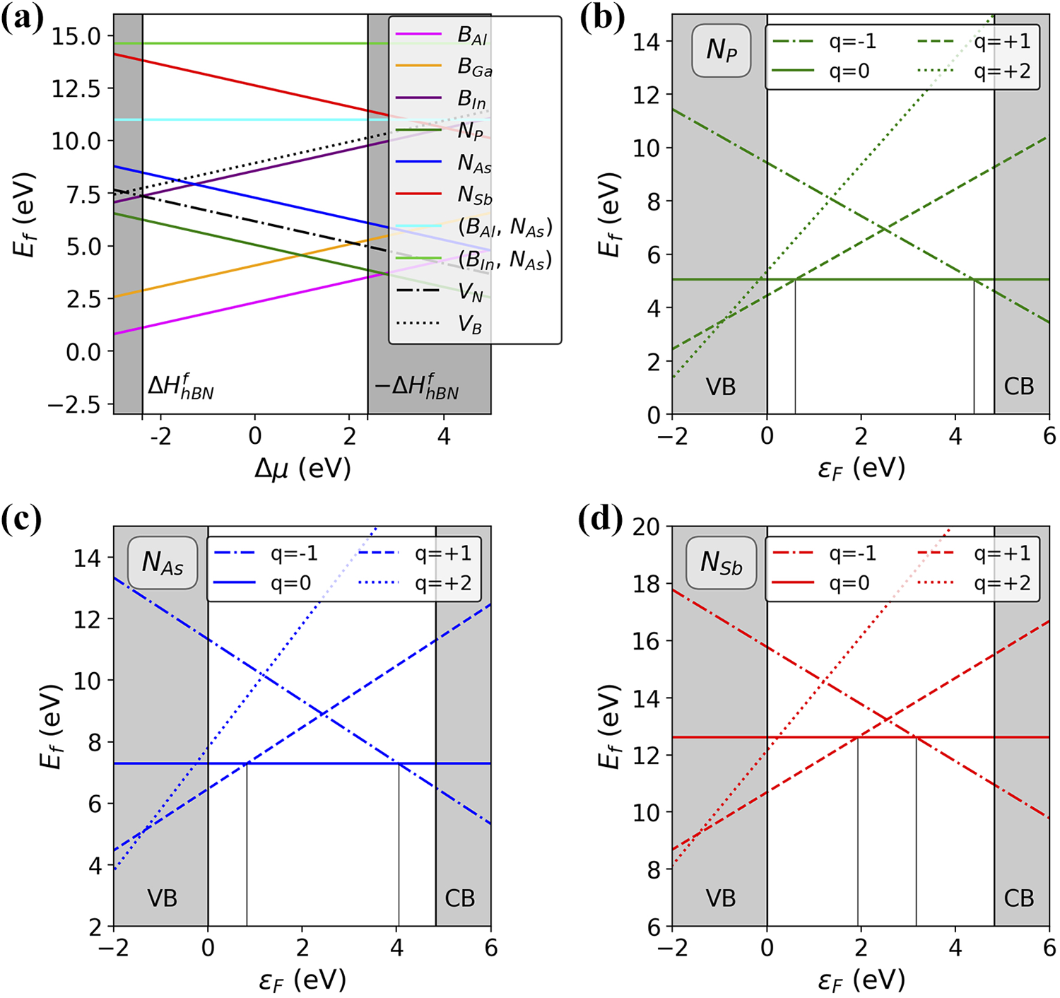
Formation energies of substitutional defects in h-BN. (a) Formation energies of substitutional defects as a function of
The hierarchies in defect formation energies are reflected by the amount of strain introduced in the h-BN lattice by the introduced heteroatom. In Figure 3, we schematically report the optimized geometries of the studied substitutional defects highlighting in color the percentage difference of each bond length with respect to the equilibrium bond length of pristine h-BN. This way, compressed bonds appear in shades of blue, ranging from 0% to −5% compression, while elongated bonds are colored in shades of red–purple, from 0% to +5% (light red) to +35% (dark purple) stretching. It is possible to notice that the most distorted bonds directly involve the heteroatom and show a significant stretching. For B-substitutions, we have +17% for N–Al bonds in BAl (panel a), +19% for N–Ga bonds in BGa (panel b), and +29% for N–In bonds in BIn (panel c), in agreement with the increasing atomic radius of Al, Ga, and In. Similarly, for N-substitutions, we found +19% for B–P bonds in NP (panel d), +23% for B–As bonds in NAs (panel e), and +31% for B–Sb bonds in NSb (panel f), again in agreement with the atomic radius trends. The variations among B–N bonds in the lattice never exceed ±5%.
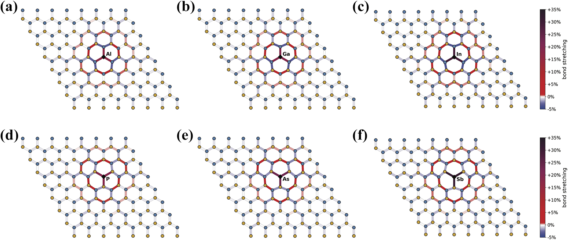
Representation of bond stretching and compression for the analyzed point defects. Bonds between atoms are color-coded according to their percentage difference from the equilibrium B–N bond in h-BN. Compression values range from 0% to −5% and are colored with blue shades, elongation values range from 0% to +35% and are colored in red–purple shades. Boron and nitrogen atoms are represented by blue and orange dots, respectively. The heteroatoms are marked by black diamonds and labeled. h-BN: hexagonal boron nitride.
For the single-substitution defects, we explored the stability of different charge states which can originate interesting features in the electronic band structure and, consequently, on the emission spectrum (see next subsection). In Figure 2, we show the dependence on the Fermi level
For each substitutional defect, we investigate the charge states q = −1, 0, +1, +2 and report the relative transition levels in Table 1. Charge state +2 is never found to be favored for values of the Fermi level within the electronic gap of pristine h-BN. The stability ranges of charge states −1 and +1 become larger while moving from P to Sb. In Table 1, we also show the calculated ionization potential
Charge-state transition levels (equation (4)), ionization potential (

h-BN: hexagonal boron nitride; IP: ionization potential; EA: electron affinity.
a The values of
Electronic properties
To rationalize the behavior of substitutional impurities, the different alignment of the defect states with respect to the h-BN bands has to be taken into account. With this aim, the electronic properties of different systems are analyzed in terms of density of states and projected density of states. The h-BN upper valence band (VB) has predominantly N-2p character with some hybridization with B-2p orbitals, while the lower conduction band (CB) has mainly B-2p character. Upon N-substitutional impurity inclusions, occupied defect states attributed to the p orbitals of P, As, or Sb appear in the h-BN bandgap located at more than +1 eV from VBM, as reported in Figure 4 (panels (d), (e), and (f)). In B-substitutional impurity inclusions, Figure 4(a), (b), and (c), only in BAl and BIn cases, an unoccupied defect state appears right below the conduction band minimum (CBm). B-substitutions, therefore, behave differently from N-substitutions in terms of electronic structure, resulting in shallow defects almost undistinguishable from the CB. This suggests that the character of the bond between the boron substitute (B
X
) and the nearby nitrogen atoms is rather similar to that of B–N bonds, thus resulting in energy levels near or fused with the CB. On the contrary, the electronic structures of N-substitutions point at a different character of the bond between the nitrogen substitute (N
X
) and the nearby boron atoms, resulting in the destabilization of energy levels, well distinct from the VB. A rough indicator of different bond characters can be found in the electronegativity

DOS and PDOS of B- and N-substitution in h-BN sample. DOS: density of states; PDOS: projected density of states; h-BN: hexagonal boron nitride.
When considering joint substitution of two adjacent boron and nitrogen atoms and two nonadjacent boron and nitrogen atoms, we observed two occupied defect states above VBM.
The electronic structure is analyzed in Table 2. For each studied system, we report the energy of the highest occupied state (HO),
Calculated energy of the HO,

HO: highest occupied state; LU: lowest unoccupied state; h-BN: hexagonal boron nitride; CBm: conduction band minimum; VBM: valence band maximum.
a In the last column, the type of electronic transition is reported. For instance, for the pristine h-BN this is the difference between CBm and VBM. For NAs this is the difference between CBm and the HO, while for BIn this is the difference between VBM and the LU.
The analysis above demonstrates that there is a strong correlation between the local anisotropic distortions and strained interatomic bonds caused by the substitutional impurities introduced in h-BN lattice, as discussed in the previous subsection, and changes in the local electronic structure. In particular, the higher the induced strain, the deeper the defect level in the semiconductor energy gap.
In addition, to understand if substitutional impurities in the h-BN matrix may give rise to defect states localized in space, we calculate the dispersion in reciprocal space and the charge densities of the states involved in the photoexcitation process (HO-1, HO, LU, and LU+1 defect states) for neutral and charged structures. Here we report only the NSb case in Figure 5. The band structures of NSb defects at different charge states are plotted in Figure 5 (panels (a) to (c)). We set
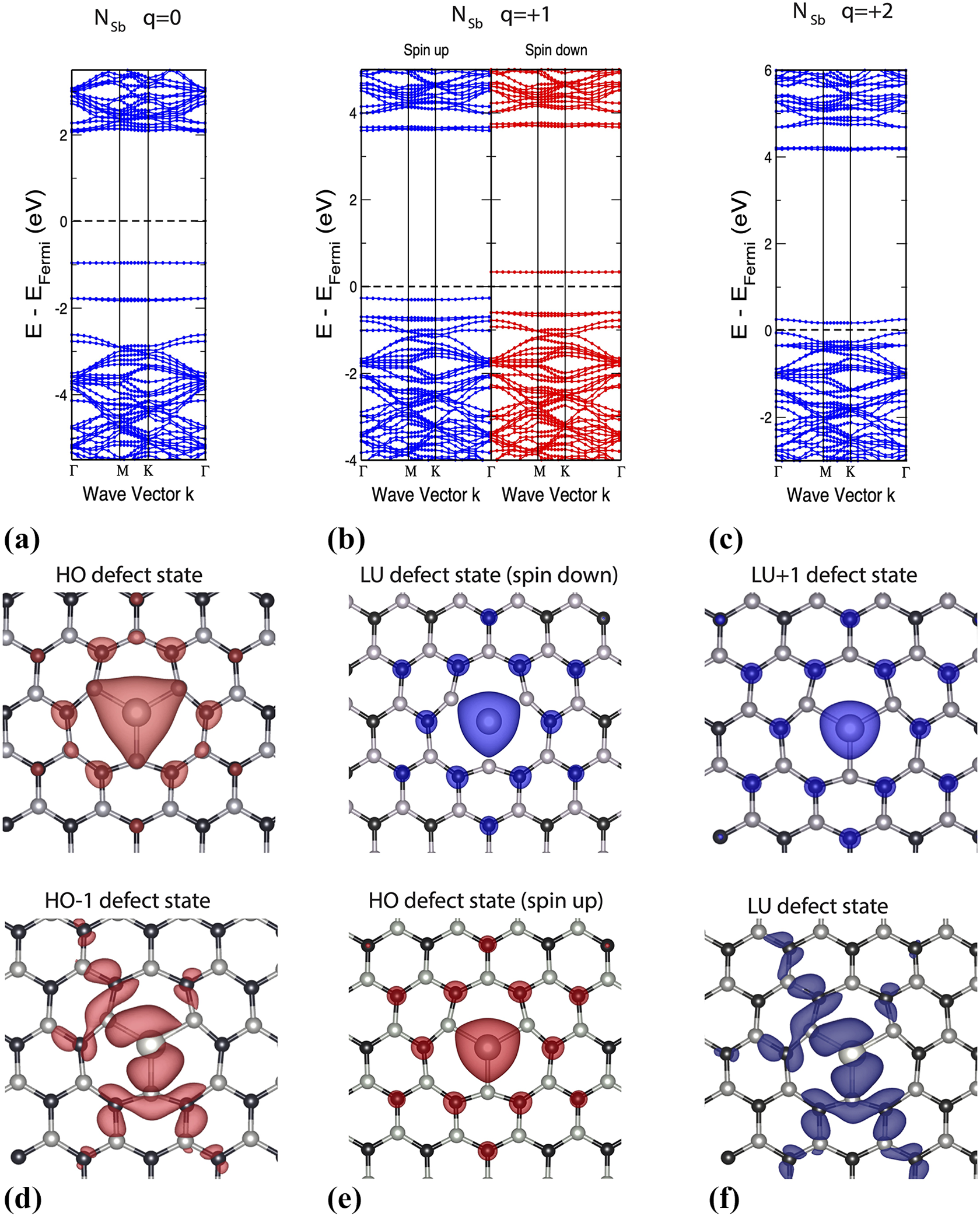
Electronic band structure of NSb samples with charge states
Conclusion
We have analyzed the energetic and electronic properties of point defects in h-BN obtained through the substitution of a boron or a nitrogen atom with a heteroatom belonging to their respective group. Period by period, the computed formation energies show that B-substitutions are generally more favored than N-substitutions and both types of defects present a formation energy that increases with the period of the heteroatom. However, although energetically favored, our study of the electronic properties points out that N-substitutions do not introduce well-defined defect energy levels within the h-BN bandgap. Rather, in these cases, the defect levels tend to coalesce with the CB. On the contrary, B-substitutions appear to generate defect levels that are deep in the bandgap of h-BN. These states are occupied for neutral defects and allow for new electronic transitions between the HO defect state and CBm that can be exploited for single-photon emission.
Moreover, the study of different charge states reveals significant stability ranges for N-substitutions in the +1 charge state, in particular for NSb. The positive charge of the defect creates an empty level with fixed spin, which becomes the new LU state. This way, new transitions may take place between the new LU state and VB states with the same spin. The different energy gaps between the HO defect state and CBm in the neutral case and between VBM and the LU states for
Our theoretical calculations show that the formation energies of all structures analyzed in this work are of the same order of magnitude of formation energies of substitutional oxygen at the nitrogen site and substitutional carbon at the boron site observed experimentally by means of X-ray absorption near edge structure (XANES) analysis as reported by Jungwirth et al. 31 This is evidence that substitutional impurities belonging to the 13th and 15th groups in h-BN may have equal likelihood to be observed experimentally. In addition, the deep defect levels introduced in h-BN bandgap by B-substitutions give rise to complementary emission wavelengths compared to substitutional impurities discussed in the literature. 28,31,33 –35 and equally useful for different kinds of applications ranging from quantum computing to information-processing technologies.
In conclusion, our results highlight that the proposed N-substitutions in h-BN can be attractive for SPE, in particular with regard to the depth of the defect level, localization of the defect state, and the tunable emission frequency, thus serving as a fruitful starting point for future theoretical studies and possible technical applications.
Footnotes
Acknowledgments
The authors acknowledge the Centre for High Performance Computing (CHPC) of the Republic of South Africa for the fundamental availability of computing resources on the high-performance LENGAU cluster. The authors also wish to acknowledge the CINECA award under the ISCRA initiatives and HPC@POLITO, for the availability of high-performance computing resources.
Declaration of conflicting interests
The author(s) declared no potential conflicts of interest with respect to the research, authorship, and/or publication of this article.
Funding
The author(s) received no financial support for the research, authorship, and/or publication of this article.