
Abstract
In this study, a compact 100-W input power light-emitting diode array vapor chamber–based plate has been fabricated to investigate the thermal performance. To make a comparison, a typical commercial chip on board–type light-emitting diode array using a copper-based plate which has the same chip layout and the same power input was also investigated. The surface temperature distribution and total thermal resistance corresponding to these two high-power light-emitting diode modules were measured using a thermal infrared camera and a MicReD T3Ster. The experimental results show that the thermal performance of the compact light-emitting diode array using vapor chamber–based plate is much better than that using copper-based plate. The average temperatures of light-emitting diode copper- and vapor chamber–based plates are 100.5°C and 41.5°C at 100 W power input, respectively. In addition, the maximal temperature difference of the 100-W light-emitting diode array vapor chamber–based plate is 2.2°C far less than 31.7°C of copper-based plate. Furthermore, the measurement results show that the vapor chamber can prominently lower the spreading resistance, diminish the hot-spot effect, and increase durability.
Keywords
Introduction
Since the 20th century, high-power light-emitting diode (LED) is keeping attracting interests due to its significant impacts on solid-state illumination industry,1,2 and it is a strong candidate for the next generation of general illumination applications. 3 However, at present, the thermal fluxes of LED chips are more than 100 W/cm2, the junction temperature of LED should be controlled below 110°C, and thermal problem caused by the heat generated within the LED itself is still a bottleneck to limit the stability, reliability, and lifetime of high-power LED. 3 The hot-spot effect and high spreading resistance result in the higher junction temperature. 3 Therefore, effective thermal design of LED packages with low thermal resistance is critical to improve the performance of LED.1,2,4,5
In order to enhance the thermal performance of the device, currently, cooling technical development related to the application of two-phase flow heat transfer assembly to thermal modules has become mature and heat pipe–based thermal module is one of the best choices. 6 Phase-change cooling is a promising method for cooling high heat flux devices. Vapor chamber is one kind of phase-change heat transfer devices using phase-change cooling method. It has already been confirmed that the vapor chamber has antigravity, high effective thermal conductivity, and is suitable for high heat flux of a heat source as the integrated heat spreader.6,7 Some research on thermal characterization of LED packages with the vapor chamber7–10 has been reported. With the power input equal or greater than 80 W of the LED illuminator and its potential for energy-saving and general illumination applications such as road and tunnel lighting, there is an urgent need for the research on thermal characterization of these new high-power packing technologies with low thermal resistance and high efficiency. However, there is lack of study for the thermal resistance effects with respect to the high-power (more than 50 W) LED array compared with common copper-based plate in natural convection cooling at ambient temperature.
In this article, a compact high-power LED array with vapor chamber–based plate has been designed and fabricated. The device surface temperature distribution of a 100-W power input LED array using a vapor chamber–based plate has been investigated using a thermal infrared (IR) camera and the MicReD T3Ster analyzer. To make a comparison, the LED array using a copper-based plate was also investigated.
Experimental methodology
Structure of 100-W LED array with vapor chamber– and copper-based plates
The vapor chamber has already been confirmed to an advanced cooling heat spreader for high heat flux of heat source. 7 It has been fabricated with low cost due to a mature manufacturing process for several local suppliers. In this study, a vapor chamber, supplied by Nanjing ACME Co. Ltd (China), made of aluminum alloy pasting LED chips array measures the thermal performance with a heat pipe radiator. As shown in Figure 1, the vapor chamber is constructed of two flat plates with 0.2 mm thickness and a frame. Its dimensions are 60 × 60 × 3.0 mm3, the interior wick structure of vapor chamber is wire mesh, and in the evaporating side are the two layers of 180-pore wire meshes of sintered metal powders and in the condensing side is one layer of 100-pore wire meshes. The wire meshes are bonded to the condensing and evaporating sides and around the internal surface to ensure the circulation of the water working fluid to form big water circulation. Several 1.8-mm-diameter porous medium aluminum cylinders supported vacuum and loading force.

The structure of the vapor chamber.
In this study, the commercial GaN-based LEDs coated with blue color (Epistar Venus-series) were used for the fabrication of an array in this experiment. The LED chips were mounted as 10 × 11 arrays by an automatic die bonder (ASM AD860) using silver epoxy die attach adhesive (DDA) on the vapor chamber–based plate. The mounted LED array area is about 24 × 24 mm2. The DDA is the silver filled epoxy of Tanaka model TS-369-E31. The thermal conductivity of the DDA is about 96 W/m K from the manufacturer’s specification. The silver epoxy DDA acts as a prominent thermal interface material (TIM) to reduce the thermal contact resistance (TCR) between the LED chip and the substrate. In order to measure the interface temperature of the LED chips, no encapsulation process was performed on the LED chip so that the chip can be exposed for IR imaging inspection and only packed with a F4R to link wire. To make a comparison, a typical commercial chip on board (COB)-type LED array using a copper-based plate which has the same chips layout was also fabricated (as shown in Figure 2). The material of copper-based plate was also made from the same 99.9% oxygen-free copper. All the LED chips were placed on the copper-based plate with the same process of the previous vapor chamber–based plate.
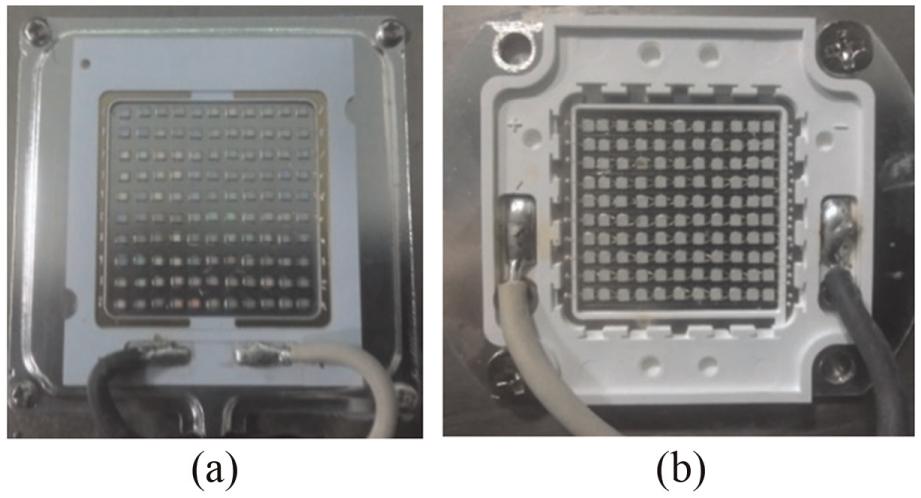
100 W LED array with (a) vapor chamber–based plate and (b) copper-based plate.
An optimized heat pipe radiator suitable for high-power electronic devices has been assembled to quickly dissipate the heat which is generated from the LED array. The dimensions of the heat pipe radiator were L × W × H = 274 × 180 × 94 mm3. The thermal resistance of the heat pipe radiator was 0.19 K/W at 100 W power input with the cooling of natural convection at room temperature 25°C. It is important to maintain approximately the same TCR between the base plate and the heat pipe radiator under the identical loading and thermal conditions; a TIM (Silanex model ST0903) has been installed between the base plates and the heat pipe radiators to reduce the TCR. A 500 meshes of steel wire mesh (about 24 µm in hole-diameter) is used to coat the TIM onto the contact surfaces to ensure the uniform bond line thickness. The same force between the two kinds of base plate and the heat pipe radiator has been exerted by the torque wrench with several tightened bolts. The thermal conductivity of the TIM is about 30 W/m K from the manufacturer’s specification. The LED array of the vapor chamber–based plate screwed with the heat pipe radiator is illustrated in Figure 3.
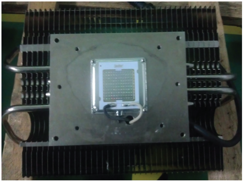
The vapor chamber–based plate screwed with the heat pipe radiator.
Experimental setup
Thermal surface measurements of the two kinds of base plate LED arrays have been achieved with a Fluke Ti32 uncooled thermal IR camera. All the tests are conducted in a JEDEC standard test chamber which is the normal environment with the same heat pipe radiator cooling by natural convection at ambient temperature of 25 ± 3°C. 11 The thermal path (junction-to-case) is determined by the transient thermal analysis using the MicReD T3Ster analyzer. 12 The power input was exerted by a direct current (DC) power supply (Agilent 6675A). The operating voltage is fixed at a constant level of 33.3 V, and the input current is 3 A.
Thermal resistance mode
In the case where the above-mentioned LED array thermal module has been cooled effectively by a vapor chamber–based plate, the whole system was at an effective heat transfer state compared to that of a copper-based plate. To compare the difference in thermal resistance, both modules with the optimized heat pipe radiator are measured by a T3ster analyzer. Geometrical configurations and materials of different layers of the LED module are presented in Table 1 and Figure 4. As illustrated in Table 1, according to the empirical formula for the effective thermal conductivity of the vapor chamber, its thermal performance can be calculated as 7

where
Dimensions and materials of packaging layers of the testing LED module.

DDA: die attach adhesive; TIM: thermal interface material.

The equivalent thermal resistance model of both the copper-based plate module and the vapor chamber–based plate modules.
As illustrated in Figure. 4, the equivalent thermal resistance network model of both copper-based plate and vapor chamber–based plate module is shown. Thermal conductivities of the materials used in this study are given in Table 1. Note that the volumetric heat source term, q, applies only on the 10 × 11 chip array (cf. Figure 2) and is assumed to be uniformly distributed in each chip unit. In the thermal resistance network model, from the junction temperature of LED Tj to the interface temperature of the LED chips is the thermal path of A to B. The silver epoxy DDA model Tanaka TS-369-E31 (96 W/m K) was applied between the LED device and base plate as the DDA (B to C). The thermal path of E to G is the thermal resistance of the vapor chamber–based plate or copper-based plate. The Silanex model ST0903 (30 W/m K) thermal paste is used between the base plate and the heat pipe radiator (D to E). The thermal path of E to G is the thermal resistance of the heat pipe radiator. The thermal resistance of the heat pipe radiator is in the range of 0.1–0.2 K/W; the value is tested to be about 0.19 K/W by a wind tunnel at the heat load of 100 W and cooling by natural convection at ambient temperature of 25°C.
Experimental uncertainty
An uncertainty analysis is conducted to determine the maximum error for the heat transfer performance of the high-power LED array thermal module. The uncertainty of surface temperature measurements for Fluke Ti32 uncooled thermal IR camera was reported by the producer as ±2°C. All thermocouples used in this experiment are T-type with an experimental uncertainty of ±0.5°C. The uncertainty of input power Q is less than ±0.5 W.
Experimental procedure
The experimental test was performed to investigate the thermal performance of the high-power LED array thermal module. A series of tests are carried out for the following conditions:
For thermal test, the rate of heat transfer to the LED array is calculated from the following relation:
13
After the high-power LED array thermal module has been placed in the JEDEC standard test chamber, turn on the power supply to offer LED power input. One can record the measuring data when the entire test system is kept on for about 3 h and reaches a steady state.
Results and discussion
Thermal measurements
Figure 5 presents the measured values of the thermocouples at C and E points of the two kinds of base plate LED array. These values show the temperature responses of both copper-based plate module and vapor chamber–based plate module driven at 100 W power input. In both the cases, the heat flux of single chip is about 1 × 10⁶ W/m2 which is calculated by the chip sizes (1 × 1 mm2) and input power (1 W). It can be seen that the temperature difference between C and E points of the vapor chamber–based plate is much smaller than that of the copper-based plate. The surface temperature of evaporation and condensation at the vapor chamber is less than that of the copper-based plate. As illustrated in Figure 5, the surface temperature difference between evaporation and condensation increased with time before the startup of the vapor chamber–based plate. Thus, the vapor chamber starts up at a certain temperature difference. The measured values of the thermocouples at C point and the temperature difference between C and E points of the copper-based plate increased with time. Compared with the copper-based plate, the vapor chamber–based plate spends less time to startup. The recorded data also illustrated that the vapor chamber–based plate is kept on for about 500 s and reaches a steady state.

Startup of both copper-based plate module and vapor chamber–based plate modules driven at 100 W power input.
Thermal surface measurements
Figure 6 shows the device temperature distribution of the 100-W LED array using vapor chamber–based plate. The thermal IR camera result shows that the surface average temperature difference of the 100-W LED array vapor chamber–based plate is about 41.5°C, and the maximal temperature difference is 2.2°C. The maximum surface temperature recorded is 42.3°C. It can be seen from Figure 6 that the printed circuit boards (PCBs) on the basis of FR4 have a very low thermal conductivity of 0.23 W/m K and result in high surface temperature.

Thermal surface recorded temperature of the 100-W LED array using vapor chamber–based plate.
Figure 7 presents the device temperature distribution of the 100-W LED array using the copper-based plate. The thermal IR camera result shows that the surface average temperature difference of the 100-W LED array using copper-based plate is about 100.5°C, and the maximal temperature difference is 31.7°C. The maximum temperature recorded is 121.2°C which is almost exactly of the sustainable maximum junction temperature of 110°C.

Thermal surface recorded temperature of the 100-W LED array using copper-based plate.
As Figures 6 and 7 shows the temperature of the F4R packaging material up to 120.4°C also, in this paper we research the temperature distribution of the LED array using different base plate materials instead of discuss the problem of packaging. Figure 8 shows the five-point temperature of 100 W LED array devices using the copper-based plate compared with vapor chamber–based plate. The five points are the four corners device and center device, respectively. The thermal performance of 100 W LED array using vapor chamber–based plate is significantly better than the copper-based plate. The maximum surface temperatures of LED devices on the copper-based plate and the vapor chamber–based plate are 121.2°C and 42.3°C at 100 W, respectively. Although the thermal conductivity of 99.9% pure copper is about 380 W/m K, the hot-spot effect of LED copper-based plate is obvious.
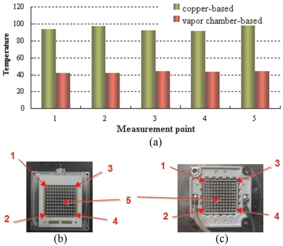
(a) The temperature distribution of copper-based plate versus vapor chamber–based plate. (b) Measuring points of LED array vapor chamber–based plate. (c) Measuring points of LED array copper-based plate.
Thermal path measurements
As illustrated in Figure 9, it is observed that the total thermal resistance of the vapor chamber–based plate module is about 0.38 K/W, less than double that of the copper-based plate module with over 0.84 K/W. There is a significant decline in thermal resistance to applying the vapor chamber–based plate (presented by the curve from point B to G in blue color) than the copper-based plate (from point B to G in red color). It also suggests that the thermal resistance path of the curves from C to D (in blue color and red color) shows that the vapor chamber–based plate has greater thermal spreading performance than that of the copper-based plate. As Figure 9 shows, the thermal resistances of the vapor chamber–based plate and copper-based plate are 0.12 and 0.25 K/W, respectively. These values are consistent with the measured data by the thermocouples. In this study, the thickness of both plates is 3 mm. Studies by KS Yang et al. 14 and CT Yang et al. 15 indicated that, for a concentrated heat source, the thermal spreading resistance is more significant for thinner plates because the adiabats extend more in the lateral direction. The thermal spreading resistance is defined by the temperatures on the heated surface as shown 14

where
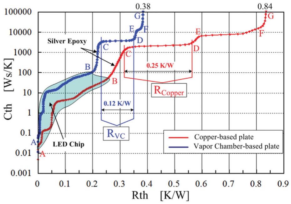
Cumulative structure functions of both copper-based plate module and vapor chamber–based plate modules driven at 100 W power input.
Conclusion
In this study, a compact 100-W high-power LED vapor chamber–based plate has been designed and fabricated. The temperature distributions are investigated and compared with a compact 100-W high-power LED array copper-based plate using a thermal IR camera and a MicReD T3Ster analyzer. The experimental results show that the thermal performance of the compact LED array vapor chamber–based plate is much better than that of the LED array copper-based plate with the same heat pipe radiator in natural convection. And the average temperatures of LED copper- and vapor chamber–based plate are 100.5°C and 41.5°C at 100 W, respectively. In addition, 100 W LED array vapor chamber–based plate is 2.2°C less than 31.7°C of the 100-W LED array copper-based plate for the central wall temperature of the lighting side. Thus, the vapor chamber provides a recommendable thermal management approach to solve the heat dissipation of the compact high-power LED array at not less or equal to 100 W electric power input. Furthermore, the measurement results show that the vapor chamber can effectively lower the thermal spreading resistance and work out the hot-spot problem. Thus, the vapor chamber provides an excellent thermal management base plate material to solve the heat transfer of the compact high-power LED array.
Footnotes
Academic Editor: Mohammad Reza Salimpour
Declaration of conflicting interests
The author(s) declared no potential conflicts of interest with respect to the research, authorship, and/or publication of this article.
Funding
The author(s) disclosed receipt of the following financial support for the research, authorship, and/or publication of this article: The authors acknowledge the financial support provided by National Natural Science Foundation of China (Project No. 51506033), Guangxi University of Science and Technology research projects (Grant No. KY2015ZD045), and Guangxi’s Key Laboratory Foundation of Manufacturing Systems and Advanced Manufacturing Technology and Innovation Project of Guangxi Graduate Education (No. YCBZ2015037).