
Abstract
A facile process for controllable fabrication of wetting surfaces with variable hierarchical structures on metallic substrates is proposed in this study. This process, which combines the through-mask electrochemical micromachining with hydrothermal growth method, could be applied on all kinds of type and size of conductive metal. First, the anodic dissolution process is predicted using numerical simulation and experiments. The formulation of electrolyte and the etching conditions in through-mask electrochemical micromachining are optimized. Ordered microstructures and smooth etched surface in large scale are obtained using the optimized parameters. Moreover, a technology has been explored to obtain various styles of multi-level structures through an alignment system or combining with a hydrothermal method of growing ZnO nanorods. The wetting effects of the rough three-dimensional surfaces are evaluated using a contact angle system. Furthermore, the wetting and the preliminary friction reduction effects of the rough three-dimensional surfaces are evaluated using contact angle system.
Keywords
Introduction
In recent decades, a great attention has been given on superhydrophobic phenomena due to its potential application in wide areas, such as self-cleaning windows,1,2 water-proofing cloths and textiles,3–5 windshield, roof tiles, and anti-biofouling surfaces.6,7 Superhydrophobic cases observed in flora and fauna provide an example that the physical topology of surfaces plays an important role in affecting the wettability of the materials. However, it has been mentioned that surface chemical properties and its roughness governed the wettability of a solid surface.8,9
Metallic substrates are widely used in aviation, aerospace, automotive, machinery manufacture, shipbuilding, and chemical industries as a result of their superior physical and mechanical properties, such as high plasticity, easy processing, and good corrosion resistance. The formation of superhydrophobic surface on metallic substrates is of great interest to improve their performance or widen their applications.10,11 In recent years, researchers have attempted to fabricate superhydrophobic surfaces through various techniques on metal substrates, such as electro-deposition,12,13 chemical etching, 14 sandblasting process, 15 oxidation, 16 chemical synthesis,17,18 and immersion processes. 19 For example, the achievements in the fabrication and application of metallic surfaces with special wettability were presented in the review article. 11 Frank et al. 15 used a process consisting of chemical etching and sandblasting to fabricate superhydrophobic surface on stainless steel and obtained a surface with high contact angle (CA) and sliding angle (SA). Liao et al. 20 fabricated textured aluminum using continuous chemical etching and extended the research of superhydrophobic surface to the anti-icing field. Wang and Xiong 21 investigated the corrosion behavior of superhydrophobic steel surfaces obtained by sol–gel method. Zhiqing Yuan et al. 22 used a combined template and etching method to transfer the hierarchical multi-scale structure of natural species onto a copper foil for superhydrophobicity. Chen et al. 23 fabricated nanocone array structure on nickel surface by electrodeposition. Guo et al. 24 developed a simple thermal oxidation method to obtain superhydrophobic titanium surface and realized the switchable property of water adhesion by controlling heat temperature and time. It is worth noting that these surface structures were not periodic and could not be controlled in a large scale. In addition, the controllability of the structures is the prerequisite for obtaining tunable wetting behaviors from hydrophilicity to hydrophobicity and superhydrophobicity. Laser technique is another way to obtain texture on metallic substrates which usually consumes long time for large-area fabrication. 25 Meanwhile, the hierarchy of the structures is a guarantee of superhydrophobicity with high CA and low SA. However, most of the previous studies were focused on the silicon surface and seldom method was applied to metallic surface obtaining periodic hierarchical structures (HSs). Therefore, developing more convenient and cost-effective methods of fabricating micro/nano-HSs over large areas for metallic substrates is necessary.
Thus, the goal of this research is to obtain tunable wetting surfaces on tin–bronze substrate and to reduce the friction drag of the surface using proper texturing technique. In order to obtain the goal, microstructures with good surface roughness are obtained using the through-mask electrochemical micromachining (EMM) method. EMM is then explored to fabricate the two-level microstructures through an alignment system based on computer micro-vision developed for multi-level lithography. On the other hand, the HSs are obtained by introducing nanopillars of ZnO on the micro-textured surfaces through a hydrothermal method. Moreover, the CA and the SA on the textured surfaces are measured using a CA system.
Principle and mechanism
Superhydrophobic principle
Wettability is a fundamental property that reveals the chemical structure and its surface topology of the material. However, surfaces can be divided into hydrophilic (θ < 90°) surfaces and hydrophobic (θ > 90°) surfaces depending on the CA, θ, measured by water. These surfaces can also be categorized into superhydrophilic and superhydrophobic surfaces in the extreme condition. However, superhydrophobic surfaces attract more attention as it characterizes completely non-wettable surface (typical θ > 150° and contact angle hysteresis (CAH) < 10°). Two different regimes can be distinguished depending on the dimension and level of surface roughness (Figure 1).
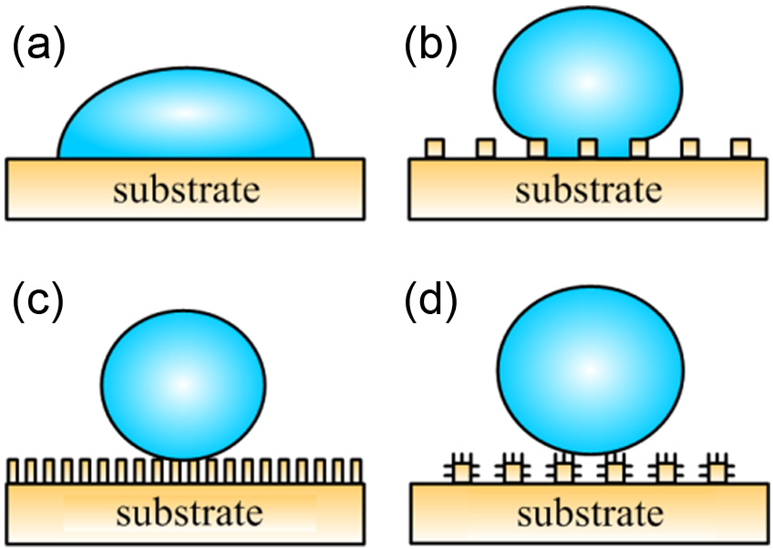
Liquid droplet spreading on (a) flat substrate and (b–d) rough substrate. Depending on the roughness of the substrate, the droplet could be either in (b) the Wenzel regime or (c) and (d) the Cassie–Baxter regime.
Mechanism of through-mask EMM
EMM is a controlled anodic dissolution process where the workpiece and the tool are considered as anode and cathode, respectively. During through-mask EMM process, metal dissolution takes place at the anode surface lying at the bottom of a cavity created by the patterned photoresist mask. The current distribution at the electrode is thus dictated by the photoresist artwork parameters. Figure 2 shows the scheme of simplified through-mask EMM process used for numerical calculation in which h is the etched depth, d is the thickness of the photoresist mask, and wr and wa are the width of the covered and exposed electrode surfaces, respectively. The parameters, those characterizing the shape evolution during through-mask EMM, are defined as follows: (1) aspect ratio of photoresist mask pattern, ras = d/wa; (2) spacing and opening ratio, rso = wr/wa; and (3) aspect ratio of the etched concave, rec = h/wa.
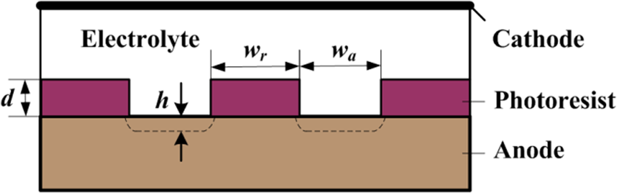
Schematic of the simplified EMM processes.
The simplified two-dimensional (2D) model geometry consists of two electrodes (cathode and anode), two photoresist mask domains, and an intermediate electrolyte domain (Figure 2).
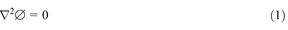
According to the electric field theory, the electric potential distribution in the electrolyte is governed by the following Laplace’s equation
where
where
The current density, I, is given using Ohm’s law

The etching rate, v, at which the anodic surface recedes, is determined using Faraday’s law
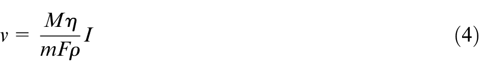
where M is the molecular weight of the metal used as anode, m is the metal dissolution valence, ρ is the density of the anodic metal, F is Faraday’s constant (F = 96485 C/mol), and η is the current efficiency of the metal dissolution.
Experiments
Sample preparation
Mirror-polished tin–bronze disks (30 mm diameter, 3 mm thickness) were used. All samples were consecutively rinsed in acetone, ethanol, and deionized water. Thereafter, the samples were dried with pure nitrogen, baked on a level hot plate (100 °C) for 10 min to evaporate the residual water. Then, the samples were cooled and enclosed in dry airtight container.
Through-mask EMM process
Typical through-mask EMM process involves two steps: fabricating patterned mask and electrochemical etching. For planar surface, the patterned mask is usually obtained using lithography method. In this study, a thin layer (about 2–4 µm) of positive tone photoresist (EPG 533; Everlight Chemical Industrial Co., Taiwan) is spin-coated and baked at 75 °C for 5 min to evaporate the solvent and to densify the film. Then, it was exposed under ultraviolet (UV) using an exposure machine (ABM Inc., Asia Pacific Ltd, USA). The development of the resist is accomplished in 1 min by immersing and agitating the exposed sample into the developer (5 wt% NaOH). Following rinsing in deionized water and drying by N2 gas, the resist is hard baked at 100 °C for 15 min to obtain good mechanical properties.
The setup for the electrochemical etching is illustrated in Figure 3. The sample to be etched serves as the anode and is attached to an insulation holder. An aluminum plate is used as the cathode. A pulsed voltage of 10 V is applied between the anode and cathode. Both electrodes are facing each other with a gap of 40-mm electrolyte (25 °C) which is stirred with an ultrasonic agitator during etching.
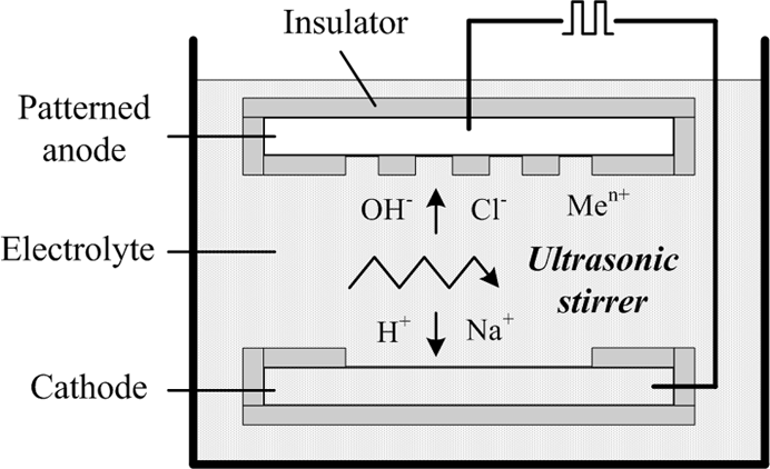
Sketch of the through-mask EMM setup.
Fabricating process of ZnO nanopillar arrays
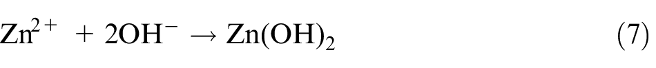
The fabrication of well-aligned ZnO nanopillars mainly includes three steps. First, crystal solution of ZnO seed was prepared using colloid method where zinc acetate dihydrate (Zn(CH3COO)2·2H2O) and sodium hydroxide (NaOH) are dissolved in ethanol. The concentration of zinc acetate dihydrate and sodium hydroxide in the resulting solution is 20 mM (mmol/L) and 40 mM, respectively. The resulting mixture was agitated at 60 °C for 30 min to yield a homogeneous and stable colloid solution, which serves as a coating solution. Second, the cleaned workpiece was submerged in the colloid solution for 5–10 min, and then baked at 120 °C for 5 min. The process was repeated for three times to make sure that the surface seed crystal layer is well prepared. Finally, ZnO nanopillar arrays were synthesized on seed crystal layer using a hydrothermal method. The aqueous solution was a mixture of zinc nitrate hexahydrate (Zn(NO3)2·6H2O, 25 mM), hexamethylenetetramine (HMT; C6H12N4, 25 mM), and deionized water (500 mL). The ZnO nanopillars were then synthesized at 95 °C for 3 h. The mechanism of chemical reaction is as the following equations (5)–(8)


Surface low-energy modification
All the samples were soaked in the solution of 1,1,2,2-tetrahydroperfluorodecyltrimethoxysilane (CF3(CF2)7CH2CH2Si-(OCH3)3 (CAS No. 83048-65-1, SICONG®)) with a concentration of 0.8%. After that, the samples were baked in an oven at 200 °C for 60 min to evaporate the solvent. Then samples were covered with low-energy self-assembled monolayers (SAMs). The surface wettability characterized by CA and SA is measured with CA apparatus (OCA20; Dataphysics, Germany) on smooth and textured surfaces.
Results and discussion
Numerical simulation
Finite element analysis (FEA) software (COMSOL Inc., USA) is used in this study. Operation conditions have been determined by trial-and-error method. The trial-and-error method can be described as follows: the computing domain is divided into a series of small triangular elements and the meshes in the domain near the anode surface have been refined locally; the time step is 0.1 s. The etching rate of the anode is obtained by defining the rate of the deformed moving mesh using arbitrary Lagrangian–Eulerian (ALE) method in accordance with equation (3).
The material parameters are described as follows: electrical conductivity of the electrolyte and photoresist mask is 10 S/m and 1.0 × 10⁻⁸ S/m, respectively. The anode and the cathode used were copper metal where the volume electrochemical equivalent, ω, is equal to 3.7 × 10⁻¹¹ m3/A.S. The electric potential of the anode U = 2 V, where V is the voltage unit. It should be mentioned that the current efficiency, η, was assumed to be 100%. The simulation results keep good agreement with the results of FEA. 26
Effect of the aspect ratio of mask pattern on current distribution
In this section, the aspect ratio of mask pattern (ras) is selected as 0.05, 0.1, and 0.5 for simulation. Figure 4 shows the simulating results. When ras is very small, the current density mainly concentrates on the edge of mask patterns resulting in construction of limbic pit and central bulge. As ras increases, the current density difference at the patterned anode becomes smaller. For example, when ras is chosen as 0.05, the current density on the edge and middle of mask patterns at the anode surface is found to be 40,000 and 15,000 A/m2, respectively. When ras is increased to 0.1, the current density becomes 30,000 and 16,000 A/m2 on the corresponding area, respectively. On the other hand, when ras is selected as 0.5, the current density at the opening of the anode basically distributes uniformly and the difference is found to be very small.
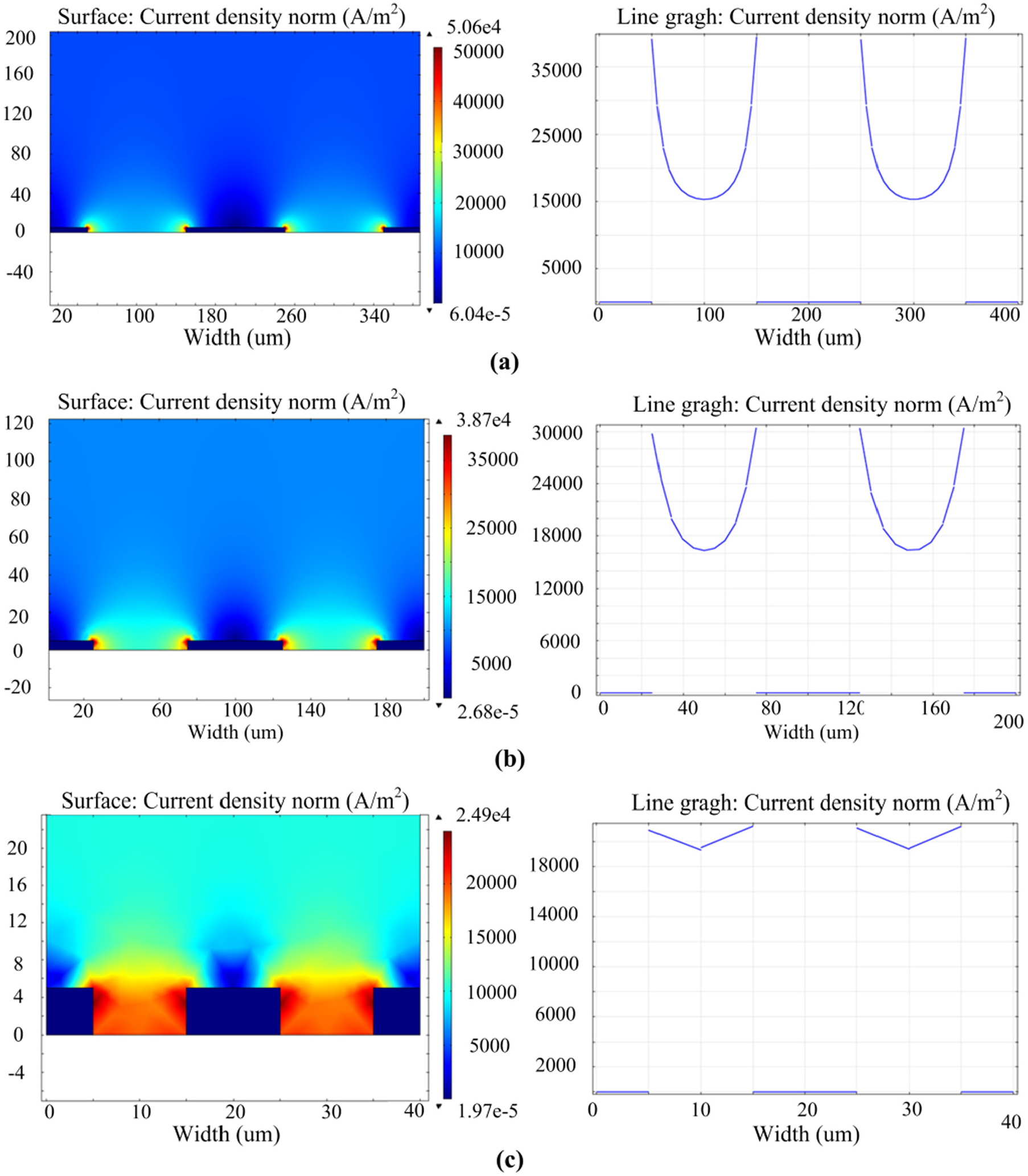
Distribution diagrams and magnitude of the current density at anode surface using different aspect ratio of photoresist: (a) ras = 0.05, (b) ras = 0.1, and (c) ras = 0.5.
The uniformity in the current distribution between the insulating mask using a high aspect ratio (0.5) is probably attributed to the enhancement of the current scattering effect of the mask side walls. Increasing the aspect ratio of mask pattern could decrease the current density difference at the opening of the anode surface, which subsequently improves the etching uniformity and bottom quality. However, deep mask features have some disadvantages such as fabrication difficulty, and they do not facilitate the mass transportation involving the removal of reaction products and the renewal of electrolyte at the critical region. Therefore, the optimum aspect ratio of the mask should be determined according to the features’ size and fabrication feasibility of the photoresist mask.
Effect of the spacing and open ratio of the patterns on current distribution
The sample patterns usually possess inconsistent spacing and open ratios at different areas on the substrate depending on different functions in applications. Hence, studying and understanding the influence of variance of the spacing and open ratio on the etched results is important.
Figure 5 shows the diagram and magnitude of the current density at the anode surface for different aspect ratios. It can been seen that the current density at the region with a high spacing and open ratio is much larger than that at the region with a low spacing and open ratio (Figure 5). This inequality of the current density would result in a highly uneven etched profile and an unwanted performance variations device to device. Therefore, current aggregation is considered before programming the design rules, and the well-distributed structures are fundamental to avoid the diversity of the structures and the inconsistency of the devices.
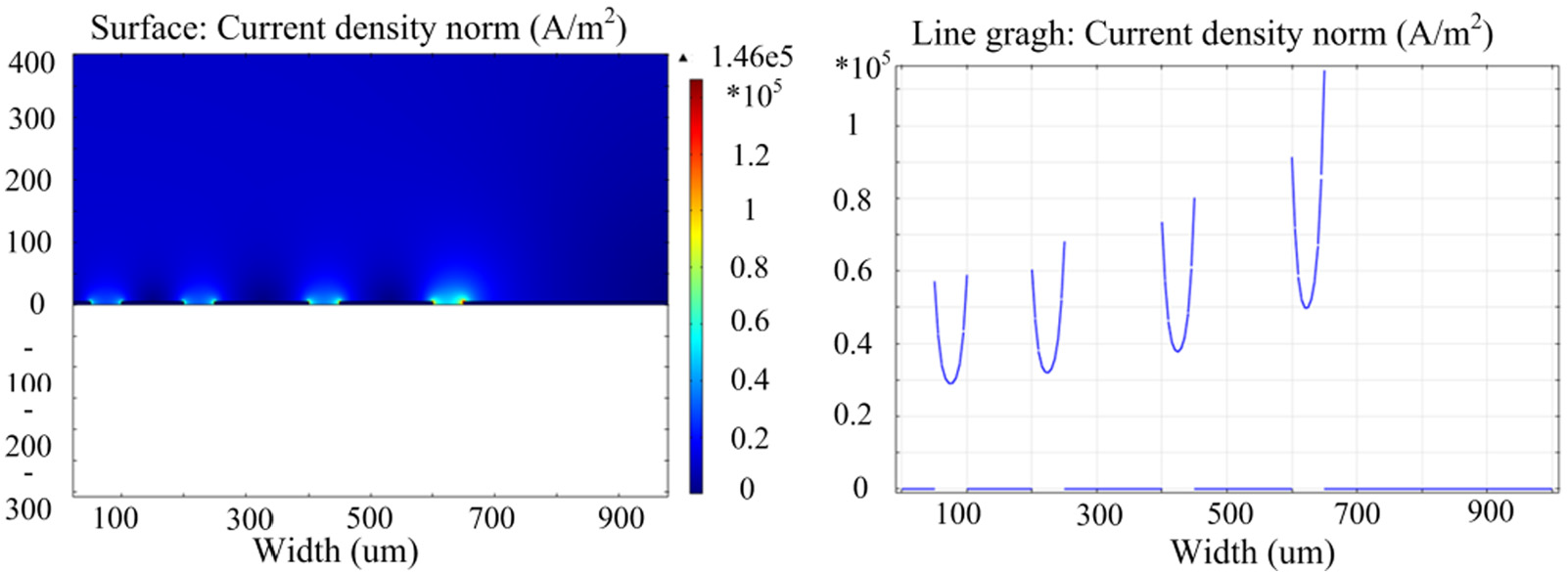
Diagram and magnitude of current density at the anode surface with respect to different aspect ratios.
Fabrication of surface micro/nanostructures
Electrolyte and power source are the most important factors influencing the etching quality. Therefore, etching conditions are required to be optimized in order to improve the etching results. During optimization, one parameter is varied keeping others constant to see its effects. The optimized etching parameters are mentioned in section “Through-mask EMM process.” The electrolyte is a neutral salt solution with the compositions of 10 wt% NaNO3 + 10 wt% NaCl. Typical etched morphology of tin–bronze substrates is shown in Figure 6. Figure 6(a)–(c) shows the images before process optimization, while Figure 6(d) and (e) indicates the images after process optimization. It can be found that both surface roughness and uniformity of etched structures greatly improved after process optimization. The etched bottom surfaces are much rugged before process optimization than the surfaces after optimization. In addition, the size accuracy of the etched concaves is also improved after optimization (the feature diameter is about 50 µm and the depth is about 24 µm before optimization, while the feature diameter is about 40 µm and the depth is about 28 µm after optimization). This proves that the optimized process could reduce dispersive corrosion and improve surface quality.
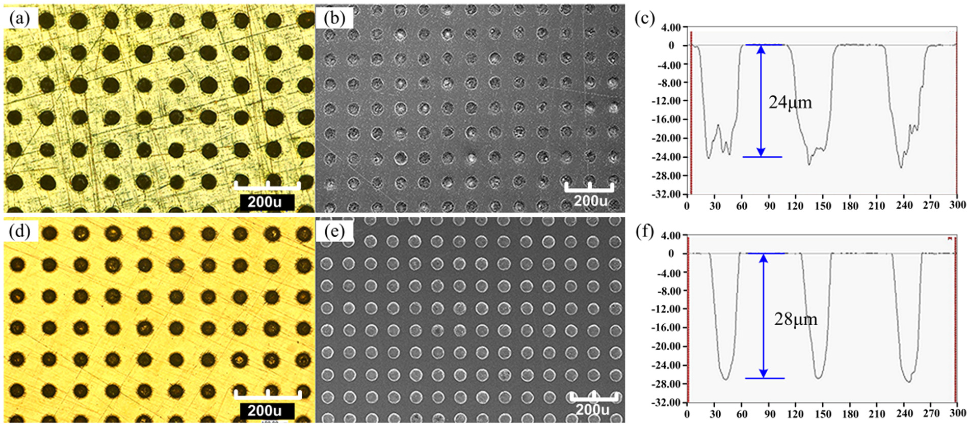
Etching result: (a) optical image, (b) SEM microstructure, and (c) transverse scanning curve before process optimization and (d) optical image, (e) SEM microstructure, and (f) transverse scanning curve after process optimization.
Dual microstructures containing two-level textures could be constructed using a combination of alignment technology of lithography and through-mask EMM after obtaining the first-level microstructures. The mask is put onto the spin-coated surface with groove patterns and laid in the orthogonal direction relative to the placement direction of the sample. Then, large-scale patterns with rectangle or square shape are conveniently fabricated in using EMM method. Different morphology could be achieved by controlling the patterned style, such as placement direction and etching time for the second time patterning. The fabrication results of tin–bronze surfaces with dual microstructures are shown in Figure 7. For Figure 7(a), the microgrooves with deep depth are etched as the first layer. The square patterned mask is used for the second lithography. Then by changing the patterned angle between the first and second lithographies as 60° and reducing the EMM etched time, three-dimensional (3D) structures with a feature size down to 20 µm are obtained. The same principle is applicable for Figure 7(b), but the microgroove patterned mask is used for both the first and second lithographies. The patterned angle is changed as 75°, and the second etched time is longer than the first time, and two-level microstructures are obtained successfully. Therefore, the application of EMM to the fabrication of dual-level structures has been explored.
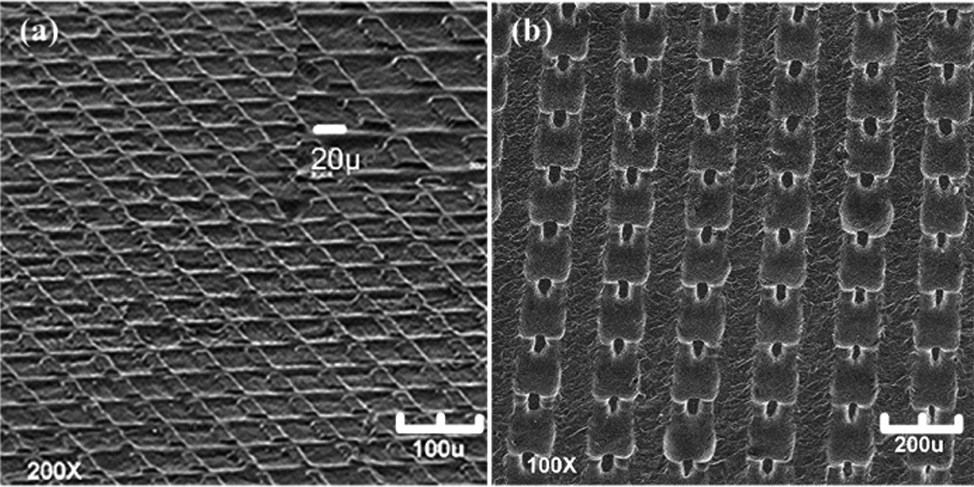
Fabrication results after two-step etching using through-mask EMM: (a) rectangle array (MM1) and (b) square array (MM2).
The HSs are believed to be the most effective way achieving superhydrophobicity. In this study, the fabrication method of the HSs on the metallic surface mainly involves two steps: etching microstructures by EMM method and developing nanostructures by hydrothermal approach. Figure 8 shows fabrication scheme of the HSs.
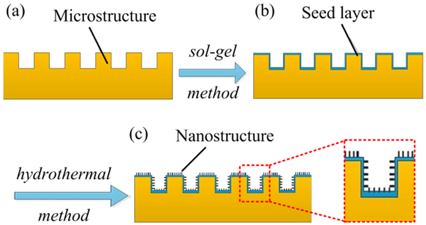
The schematic of fabricating hierarchical structures: (a) fabricating microstructures; (b) the seed layer is dip-coated on the micro-textured surface; (c) the nanostructures are grown on the micro-textured surface by hydrotermal method.
Figure 9 displays the SEM images of various structures on tin–bronze surfaces. Figure 9(a) and (c) is the surface with single-tier microstructures etched by EMM, while Figure 9(b) is the surface with single-tier ZnO nanopillars that obtained by hydrothermal growth. Figure 9(d) and (e) is the surface with the HSs corresponding to Figure 9(a) and (c), respectively. Figure 9(d) and (e) is obtained by a combination of EMM and hydrothermal method. It is evident that flower-like microspheres with a diameter of 1–5 µm are formed on tin–bronze microconcaves, as a result of etching roughness during EMM (Figure 9(d)). The magnified image of a single microflower indicates that the flower petals are composed of many ZnO nanopillars with diameter of about 50–100 nm (bottom left view of Figure 9(d)). In addition, the nanorod arrays formed on the planar surface are out of the microconcaves (bottom right view of Figure 9(d)). Meanwhile, Figure 9(e) shows another kind of the HS containing micropillars and nanorods on the whole surface. The above-mentioned fabrication results indicate that a double- or three-level roughness at micro/nanometer scale is formed during EMM and hydrothermal growth.
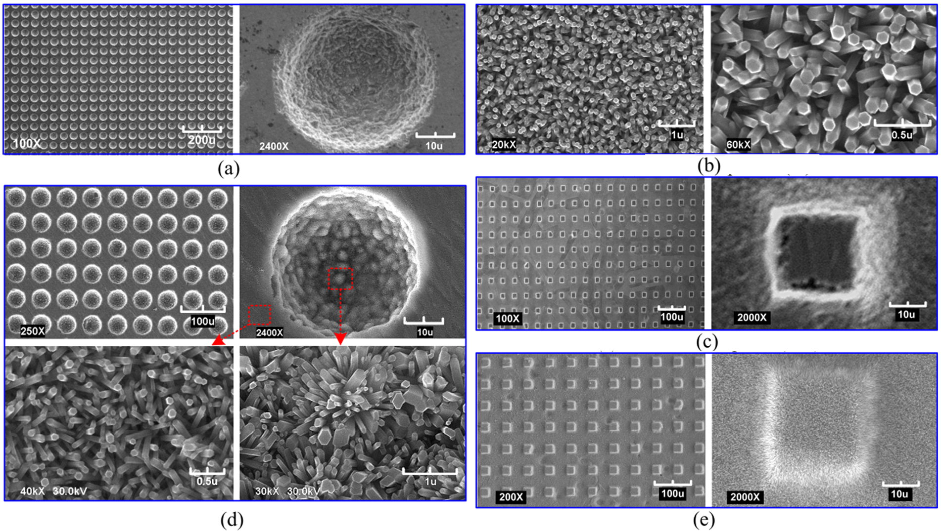
SEM images of different surfaces: (a) single-tiered microconcaves etched in EMM method (M1 surface), (b) single-tiered ZnO nanopillars obtained by hydrothermal method (N surface), (c) EMM etched single-tiered microposts (M2 surface), (d) hierarchical structures with nanopillars and microconcaves (HS1 surface), and (e) hierarchical structures with nanopillars and microposts (HS2 surface).
Surface wettability characterization
Before surface wettability test, surface treatment described in section “Surface low-energy modification” was performed to lower the surface energy. Energy dispersive X-ray (EDX) analysis was performed to check the existence of the low-energy SAMs and to study the surface chemical elements. The analysis results are shown in Figure 10, where O, F, and Si are detected after surface treatment (Figure 10(b)). It is worth mentioning that these elements are not present in original tin–bronze surface (Figure 10(a)) indicating that the low-energy film has been developed on the tin–bronze surface.
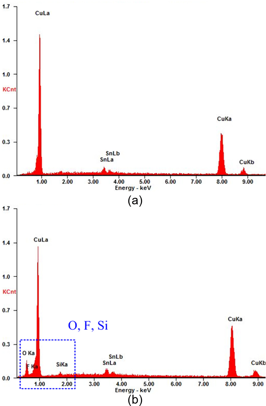
EDX results on tin–bronze surfaces: (a) before low-energy treatment and (b) after low-energy treatment.
Figure 11 shows the results of CA on various fabricated surfaces of tin–bronze substrates. The experimental results show that the hierarchical textured surfaces have the strongest water repellency (CAs > 150°), while the ZnO nanostructured surface (CA = 147.5°) and the dual micro-textured surfaces (CAs = 148.7° and 136.2°) have good hydrophobicity compared to single-level micro-textured surfaces (CAs = 100.2° and 125.1°) and smooth surface (CA = 64.2°). Thus, it can be deduced that the decrease in feature size and increase in the structure level may increase the CA in the micro-textured surfaces (M1, M2, MM1, and MM2) or nano-textured surfaces (N, HS1, and HS2). Therefore, it can be claimed that the investigated way provides an effective way to design surfaces with controllable and tunable wettability through adjusting texture pattern. However, the static angle does not adequately describe the hydrophobicity of the surface. In general, it is also required to evaluate the sliding properties of water droplets on the surface. Figure 12 exhibits the profiles of a water droplet sliding on the surface with different tier structures. The droplet sticks to the micro-textured surfaces of M1 and M2 even when the tilted angle reaches 90°. The SA is found to be about 6° for the ZnO nanostructured surface. The SA is measured to be about 2°on the MM1 surface containing dual microstructures. In the case of HS surfaces, rapid removal of large water droplet is achieved even with a slightly tilted angle of below 1°.
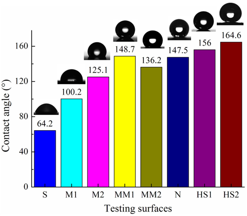
Contact angle results on different surfaces. S: Smooth surface of tin-bronze substrate; M1: microcaved surface (Figure 9(a)); M2: microconcaved surface (Figure 9(c)); MM1–MM3: dual micro-textured surface (Figure 7); N: nanostructured surface (Figure 9(b)); HS1: hierarchical surface containing microconcaves and nanopillars (Figure 9(d)); HS2: hierarchical surface containing microposts and nanopillars (Figure 9(e)).
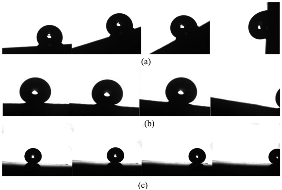
Sliding angle testing results of different surfaces: (a) sliding behavior on the MI surface: the droplet sticks on the M1 surface; (b) sliding behavior on the N surface: the SA angle is about 6° for ZnO nanostructured surface; and (c) sliding behavior on the MM1 surface: the SA is about 2°on the MM1 surface containing dual microstructures.
It should also be noted that the diameter of the concaves (M1 surface) is about 40 µm, which is beneficial obtaining a Cassie state under static contact conditions. It is clear that the CA testing results are consistent with the Cassie equation. However, when the droplet volume is too large to ignore the gravity effect (the water volume is 10 µL in the SA tests), the surface is probably in a Cassie–Wenzel transition state where the liquid would contact with partial side wall. This will increase the contact area and make it difficult to roll off the surface. In the case of HS surfaces, the droplet could get into the microconcaves under relative high external pressure, and the ZnO nanopillars on the side and bottom walls would ensure the partial contact between the top of the structures and droplet. Therefore, the HSs could provide dual guarantee for the superhydrophobicity. Therefore, it is beneficial to establish enhanced superhydrophobicity, due to the kinetics of droplet movement and the thermodynamics of wetting, through the HS.
Conclusion
This work proposed a large-scale textured surface fabrication method that could obtain controllable wettability on metallic substrates. The following points can be highlighted:
Through-mask EMM is found to be a promising technique for surface texturing.
Etching conditions and electrolyte are optimized by the experiments. Using the developed process, ordered microstructures and smooth etched surface in large-scale are obtained. In addition, two-level microstructures are obtained through an alignment system. The structures with a feature size down to 20 µm can be obtained successfully.
Wetting and preliminary friction drag reduction effect of the rough 3D periodic surfaces is demonstrated using CA system, in which textured surface containing HSs is proved to have the biggest CA (>160°) and the smallest CAH (<1°).
The experimental results show that a combination of through-mask EMM and hydrothermal method of ZnO nanostructures seems to be a feasible process for fabrication of multi-level structures and provides a valid way to obtain tunable wettability on metallic surfaces.
Footnotes
Acknowledgements
The authors thank Nanjing University of Aeronautics and Astronautics and Nanjing Tica Air-Conditioning Co., Ltd, for providing resource materials and technical support.
Declaration of conflicting interests
The author(s) declared no potential conflicts of interest with respect to the research, authorship, and/or publication of this article.
Funding
The author(s) disclosed receipt of the following financial support for the research, authorship, and/or publication of this article: This work was supported by the National Natural Science Foundation of China (Grant No. 51505219) and Jiangsu Provincial Natural Science Foundation of China (Grant No. BK20150748).