
Abstract
The study of surface texturing on a metallic surface has become a great area of interest of researchers in the last few decades. Surface texturing is employed for enhancing the performance of the surface in its working environment. As the characterization techniques have been evolving very fast, researchers have started mimicking the natural surfaces to take the advantages of their characteristics (such as self-cleaning, load capacity, reducing coefficient of friction). Manufacturing of natural inspired surface requires having a great control over the process to achieve the micro or nano features on the natural surfaces. Hence, the selection of the most suitable process and optimum parameters for machining of arrays of micro or nano features at large scale is highly desirable. This study reports an overview of different micromachining processes used for texturing on metallic surfaces and research gaps to be filled in the available literature. Electrochemical micromachining has tremendous potential on account of its versatility in different applications. It is a promising and economically viable machining process for micromanufacturing industries for fabrication of micro textures and micro features on metallic surfaces. Production of textured surface at large scale requires a sustainable technology, which can serve the purpose of enhancing the performance of the surface without changing the original properties of the surface. Indeed, laser surface texturing, through-mask electrochemical micromachining, lithography, micro- or nanocasting and so on are the existing methods which involve multiple steps for generation of textured surfaces. This article also reports some original experimental investigations for generation of different kinds of micro textures on metallic surfaces, namely, arrays of micro dimples, micro channels and micro pillars using a single-step maskless electrochemical micro-texturing process with a pre-patterned micro tool.
Introduction
Surface texturing is the process of generating a specific type of pattern on the workpiece surface in order to change its surface properties. Texturing with features on multiple scales can be produced, starting from the micro- or nanometer range extending up to millimeter range. This enables many new applications of the engineered surfaces, where specific surface texture can be used to influence functional properties, for example, wetting, tribological characteristics (friction and wear), optical properties and so on. Generally, these surfaces are referred as functional surfaces. The term “texturing” defines the engineered surfaces that contain multiple features (micro holes, micro asperities, micro dimples, micro or nano hairs, micro or nano patterns at multiple levels and so on) of exact geometrical parameters, which are purposely manufactured in order to enhance the functionality of the surface in the given environment. The content of this article can be understood from Figure 1.
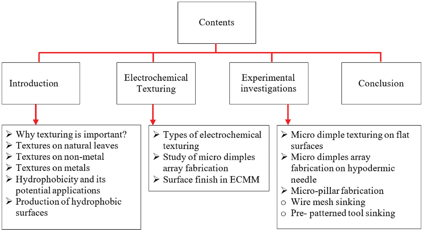
Classification diagram presenting contents of this article.
Why texturing is important?
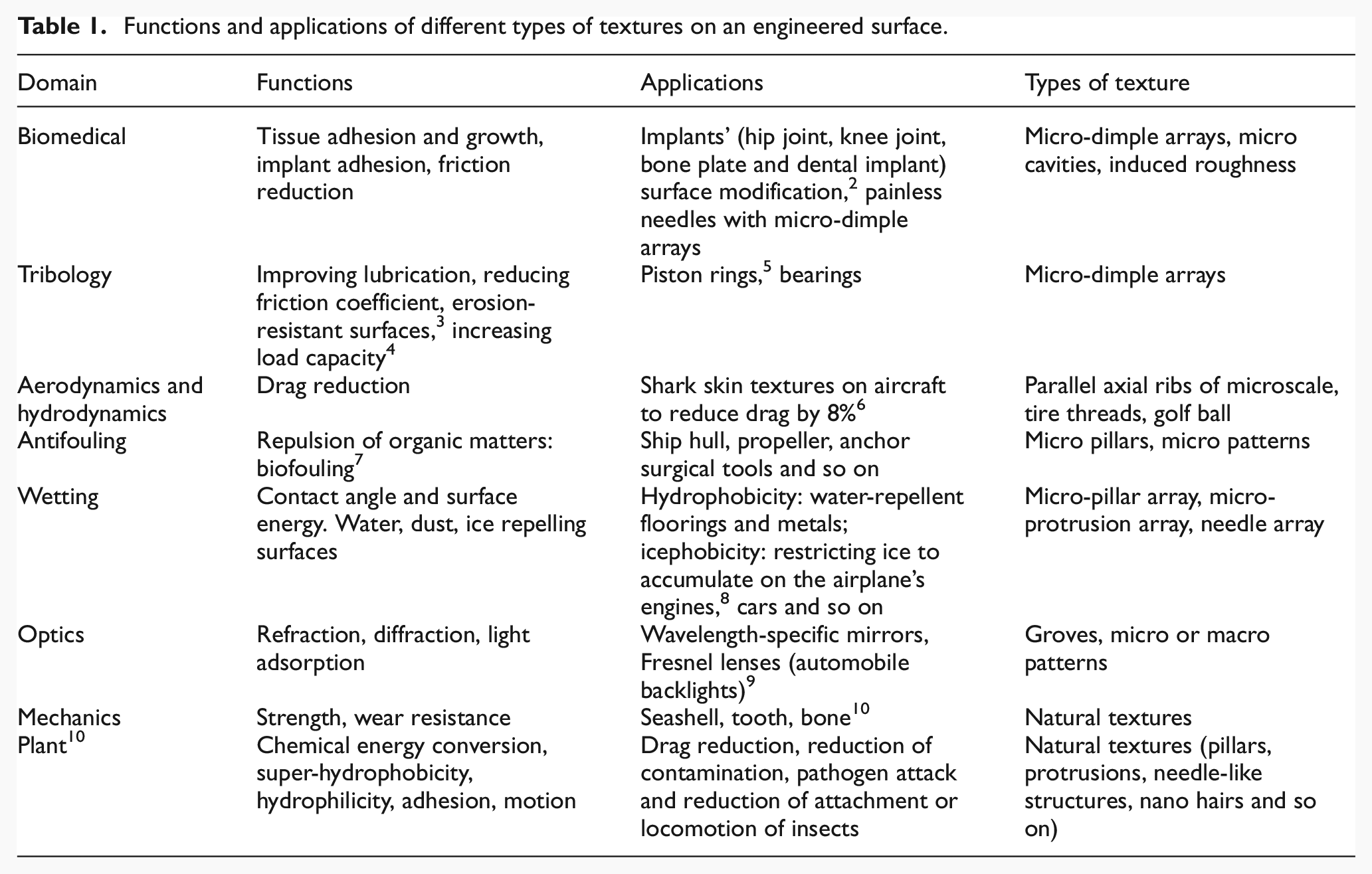
One of the ways to alter the surface properties is to generate textured surface if the target surface is intended to be used for a long period of time, and the surface is expected to perform in a violent and aggressive environment (impellers, engines of aircrafts, sliding piston–cylinder, ship hull and so on). The applications of textures are well understood with the help of the Mother Nature. For example, texture of shark skin (three-dimensional (3D) rib pattern) results in reduction in drag by a significant amount as well as reduction in turbulent wall shear stress up to 10%. 1 Moreover, a list of specific functions of different types of textures (natural and artificial) and their applications in different domains is given in Table 1, and the same is described in brief in the following sections.
Functions and applications of different types of textures on an engineered surface.
Hydrophobicity, surface free energy, interfacial free energy and surface roughness are the key parameters which influence the interaction of an implant surface with the environment inside a human body. Cell attachment and human fibroblast spreading can be regulated by manipulating the contact angle of surface of the implant.11,12
Long-term implants are defined as objects in contact with living tissues more or less permanently. In reality, the permanency might only mean several years, after which the implant needs to be replaced by the new one. These repeated critical interventions in elderly patients become more and more dangerous and life-threatening. Hence, it is a foremost existing challenge in biomaterials to develop implants that can sustain the human body for long span of time.
Biocompatibility of an implant can be increased by providing a specific surface structure which can manipulate the surface energy and contact area. The adsorption of biomolecules is the leading factor which governs biocompatibility of an implant. The environment inside a human body is typically warm (37 °C), aqueous and salty in nature. The milieux encountered by biomedical materials can be aggressive and can give rise to both corrosion and wear of implant. 2
In tribology, influence of surface texturing is being studied by several researchers using laser surface texturing (LST) and electrochemical (EC) surface texturing on various parts of a machine which undergoes high friction. Such kind of study of the effect of arrays of micro dimples on piston ring and thrust bearing is reported with the conclusion that the friction is decreased and seal life is increased. 5 The lubricating regimes may be categorized based on how the textures perform the three major roles: (1) debris trap, (2) lubricant reservoir and (3) micro hydrodynamic bearing.
The study of drag across the surface has been attempted by a large number of researchers working in the field of aerodynamics and hydrodynamics for the last few decades. The reduction in drag is beneficial in several applications; it is desirable to reduce the drag when water is flowing past the hull of a boat; air is flowing past a moving automobile; or air is flowing past the blades of a windmill fan, airfoil, fan, rotor, stator, inlet and so on.13,14 It was investigated experimentally by employing a transparent plastic film with microscopic texture. It was found that the riblets (texture of shark skin) parallel to the direction of flow help in reducing aircraft drag up to 8% which results in fuel saving up to 1.5%. 6
This article gives an overview of surface texturing responsible for wetting of surface which deals with hydrophobicity and hydrophilicity. The type and hierarchy of surface structure (surface topography) govern its contact angle with the fluid which leads to change the surface energy of the target surface. Wetting of real engineering surfaces occurs in many industrial applications (liquid coating, lubrication, printing, painting and so on). Forced and natural wetting can be beneficial in many cases, providing lubrication and, therefore, reducing friction and wear. However, the wettability of surfaces can be strongly affected by surface roughness. 12
Hydrophobicity is a property of some surfaces to repel the water, either naturally or forcefully, which leads water to barely adhere to the surface. Due to the presence of specific micro- or nanostructures on the target surface, water drops roll over the surface and bounce back while impacting them.14,15 Generally, the hydrophobicity is induced to a metallic surface by creating two levels of specific roughness (hierarchical structure) at micro and nano levels by mimicking natural hydrophobic leaves such as Nelumbo (lotus leaf), Liriodendron (magnolia), Colocasia esculenta (elephant ear) and so on.16,17 It is reported that two levels of surface roughness is a necessity for producing a surface with super-hydrophobic characteristic. For example, a pattern of conical structure with feature size of about 10 µm superimposed by a structure of sub-micrometer size. 2
Biological fouling is the aggregation of microorganisms, plants, animals and so on on the surfaces which remain in contact with water for a long time. It is reported that a significant amount of cost is associated with hull fouling. It is due to the increased fuel consumption because of increase in frictional drag generated by these accumulated biofoulings (increases fuel consumption as high as 10.3%). 18 These biological entities can be repelled in two ways: (1) fabricating mirror image of lotus leaf on metallic surfaces or (2) designing the surface in such a way that there is no direct contact between the surface and water by keeping an air film between water and metal surface. 7
Icing on the surfaces due to its environmental conditions may become a reason for numerous complications in wind turbines, roads, oil platforms, telecommunication systems, aircrafts and so on. 19 For example, while flying at high altitude, due to low temperature (~−40 °C), ice particles get accumulated on the engine of aircraft and result in freezing. Using the same concept of water repelling surface, this problem can be sorted out by making the surface super-hydrophobic so that ice particles do not get stuck on the surface.
A wetting phenomenon especially water repellency (i.e. lotus effect) has attracted attention of many researchers in the recent past. It leads to a number of excellent functions of the surfaces such as self-cleaning and protection against pathogens. It has become a trend to follow the natural surfaces so as to achieve its inherent vibrant multifunctional properties.
Textures on natural leaves
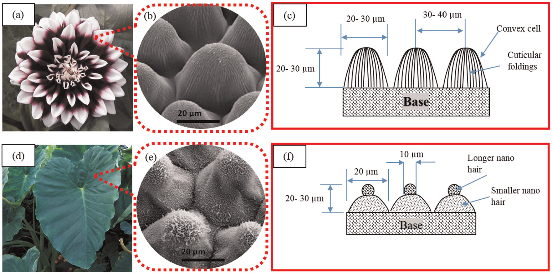
Figure 2 shows the textures available on two different natural leaves. Figure 2(a) shows the flower of Dahlia, and Figure 2(b) illustrates the structure of Dahlia flower leaf (petal) which consists of micro protrusions (diameter ≈ 20–30 µm, height ≈ 20–30 µm and spacing ≈ 30–40 µm) seen through scanning electron microscopy (SEM). 20 On these micro protrusions, second level of roughness of irregular cuticular foldings exists, whose size varies from 600 to 800 nm. Detailed specifications of these structures are presented through a schematic diagram in Figure 2(c). Cross-sectional view of the convex cells shows that height, width and space between the two cells vary from 20 to 30, 30 to 40 and 20 to 30 µm, respectively. Figure 2(d) shows an image of a leaf of C. esculenta. SEM image in Figure 2(e) shows three levels of hierarchical micro- or nanostructures. Level 1 roughness is due to micro bumps of ~20 µm diameter. Second level of roughness is obtained due to micro spheres available on the top of these micro protrusions, and third level of roughness is due to nano hairs (500–800 nm diameter) available on these microstructures. 21 These dimensional details are illustrated in Figure 2(f) through a schematic diagram. The cross-sectional schematic diagram shows combination of micro bumps of ≈20 and ≈10 µm width and nano hair.
Functions of these micro- or nanostructures can be understood by fundamental theories of hydrophobicity. Figure 3 shows interaction of droplet with a hydrophobic surface. Generally, textured surfaces demonstrate two main types of behavior: Wenzel state and Cassie state (Figure 3(a) and (b)). In Wenzel state, droplets get punctured and make a direct contact with the surface having rough structures. In Cassie state, wetting of a solid by liquid involves at least three different interfacial boundary surfaces, which are solid–liquid, solid–air and liquid–air interfaces. In wetting, when a liquid is brought into contact with a solid surface, it replaces an area of the solid–air interface by an equal area of solid–liquid interface and is also extended to the liquid–air interface. These relations vary with the topography, surface energy and surface tension of the liquid. 15
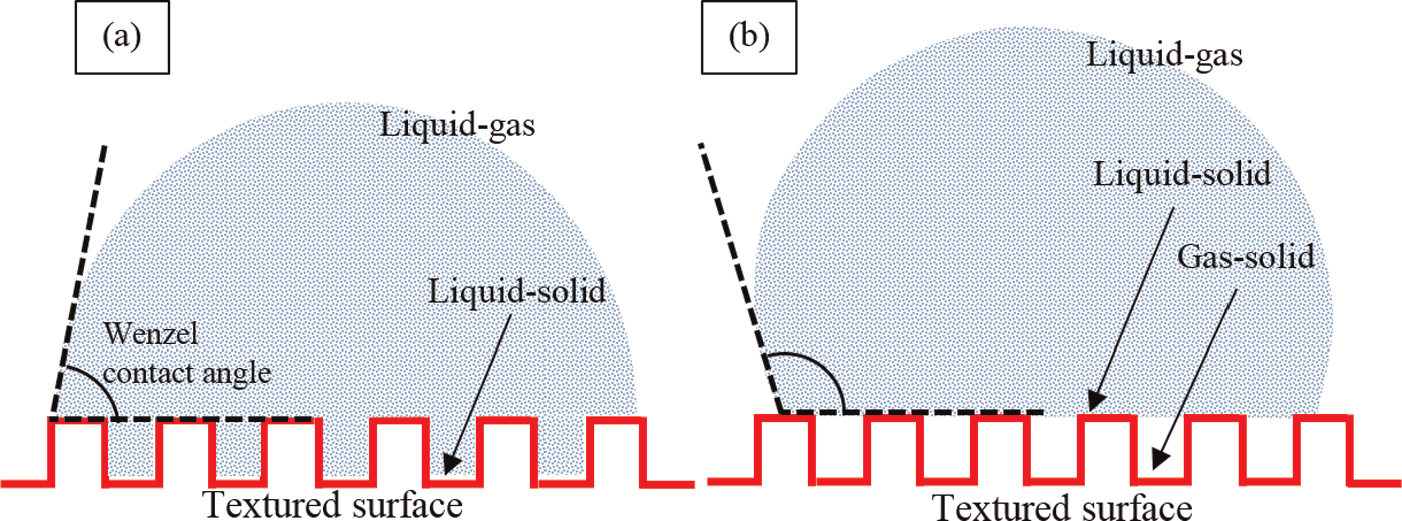
Droplet states and interfaces when a droplet interacts with a textured surface: (a) Wenzel state and (b) Cassie state.
Cassie and Baxter 22 studied another case of hydrophobicity in which liquid–solid interface is composed of two phases, that is, solid–gas interface and gas–liquid interface (as shown in Figure 3(b)). The theoretical model includes fractions of solid–liquid and air–liquid interfaces under the droplet. In general, super-hydrophobicity can be achieved when the contact angle is greater than 150 degree and the roll-off angle is lesser than 10 degree. The droplets in Cassie state can provide smaller contact angle hysteresis (roll-off angle) as well as larger contact angle. 23 The natural leaves generally consist of nano hair on the micro textures as well as base surface. These flexible nano hairs enhance the contact angle by providing a liquid–air interface between the solid–liquid interface.
Structural specifications of lotus leaf
Figure 4 shows structures of lotus leaf and size of micro or nano features of the leaf.20,24 Detailed specifications of the microstructured leaf surface are listed in Table 2. Such type of arrangement of micro protrusions (pillars) and nano hairs provide very low surface energy. This low surface energy is dominated by the surface tension of the water droplets, and the droplets try to maintain their spherical shape. Figure 4(a) shows the picture of lotus and its leaf. Figure 4(b) shows arrays of random micro pillars through SEM image present on the lotus leaf. Figure 4(c) shows a magnified view of a micro pillar, and Figure 4(d) shows nano hairs available on micro pillars of the leaf surface. Specific approximate dimensional information is incorporated in Figure 4(e) through a schematic diagram.
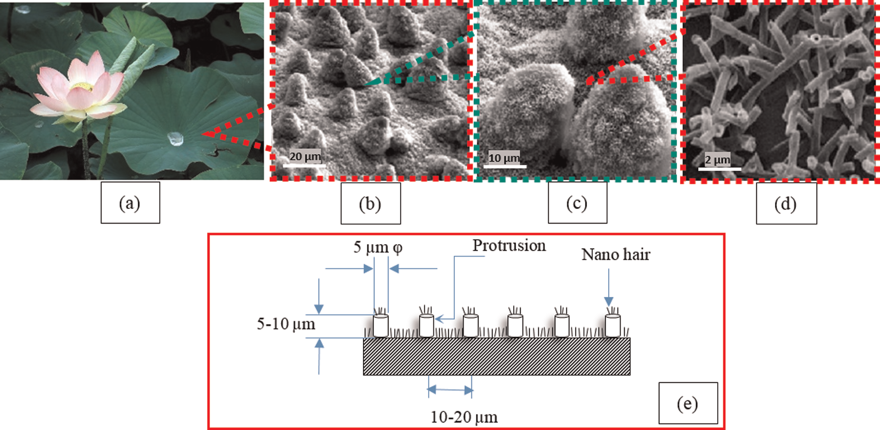
Hydrophobic lotus leaf (Nelumbo nucifera) structure: (a) computer graphic of lotus leaf (Google image), (b) SEM image showing micro-pillar array on the leaf surface, (c) SEM image showing profile of the micro pillars, (d) SEM image showing nano hairs available on the micro pillar at higher magnification and (e) schematic diagram showing configuration of micro or nano features of a lotus leaf.
Detailed specifications of micro features of a lotus leaf. 24
Micro protrusions (height ranges from 5 to 10 µm) present at random locations, support the water droplets and do not allow the droplets to get punctured. These protrusions provide contact angle of 126°. Nano hairs (height ranges from 300 to 1000 nm) are flexible and soft in nature and provide wax-like surface resulting in additional increase in contact angle by 16°. These natural micro-or nanostructures have inspired many researchers to produce hydrophobic surfaces (on metallic and nonmetallic components) so that these surfaces can give much better performance in the devices or setups.
Textures on nonmetals
Sun et al. 25 worked on nanocasting based on soft lithography nanofabrication for replication of lotus leaf. The casting process used polydimethylsiloxane (PDMS), a soft material widely used for casting to replicate the surface structures. Figure 5 shows a super-hydrophobic surface created on PDMS template through nanocasting. 25 Figure 5(a) shows the array of micro protrusions generated through casting, and Figure 5(b) shows the interaction of a droplet with textured surface. The spherical shape of the droplet shows that the surface is super-hydrophobic.
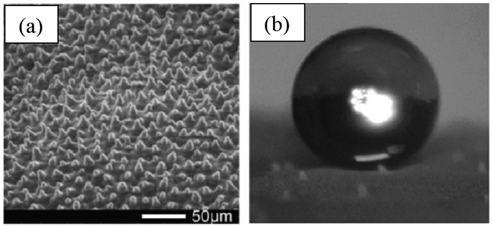
(a) SEM image of a super-hydrophobic surface and (b) droplet shape on the surface produced by nanocasting. 25
Texturing on titanium carbonitride (TiCN) coatings
Solid lubrication systems have been developed in the field of tribology to reduce wear and friction between sliding surfaces in different working environmental conditions. For providing solid lubrication on these wear-resistant protective coatings, solid lubricants need to be supplied from the reservoirs. Voevodin and Zabinski 26 demonstrated fabrication of textures consisting of micro-dimpled reservoirs on TiCN coating using precision laser micromachining. The experimental procedure is shown schematically in Figure 6. Micro reservoirs with controlled size, location and density were machined at the coated surface by a focused ultraviolet (UV) laser beam. Furthermore, lubrication tests were carried out using solid lubricants based on molybdenum disulfide (MoS2) and graphite on such micro-dimple arrays generated on TiCN coatings. It was concluded that the 10 – 20 micrometer sized features helped to retain solid lubricant availability which lead to a low cost friction and wear control over the sliding surfaces.
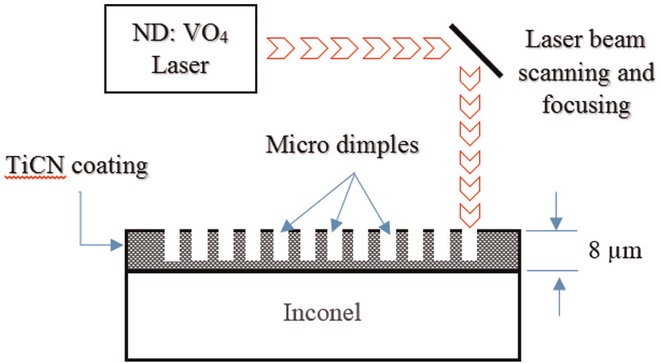
Schematic diagram of laser surface texturing arrangements to generate reservoirs for solid lubricant storage in a wear-resistant TiCN coating.
Texturing on polymer
The increasing demands for microscale devices, such as lab-on-chip, microelectronic mechanical system (MEMS), inkjet nozzles and so on, require special micromachining processes. LST is a process for micro and macro parts, and it can machine with a high level of accuracy, precision and repeatability. 27 Dayal et al. 27 proposed texturing on polymer using excimer laser by employing binary mask projection technique to reproduce the mask features from the millimeter to the micrometer range. Large arrays of 1- and 15-µm holes on Kapton are made with high resolution and uniform periodicity as shown in Figure 7. Figure 7(a) shows the image captured through optical microscopy. Each micro hole has a diameter of 2 µm, and the space between the two holes is 4 µm. In Figure 7(b), the image of atomic force microscopy shows the topography and indicates the depth of micro holes. Figure 7(c) shows a SEM image of textures of 1-µm holes with 2-µm period on Kapton surface.
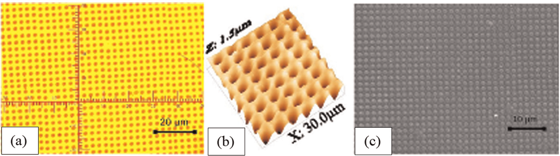
(a) Optical microscopic image of arrays of 2-µm-diameter holes with a period of 4 µm machined on a Kapton sheet, (b) AFM image showing the topography of the sample and (c) the SEM image of an array of 1-µm holes with 2-µm period. These large-scale arrays have a total array area of 1 mm × 31 mm with excellent uniformity throughout. 27
By selecting optimum parameters (such as power, beam traverse speed and beam diameter), different paths were assigned to produce micro-pillar arrays (Figure 8(a)) using CO2 laser. Figure 8(b) shows a top view of circular micro pillars through optical microscopy image (yellow circular boundaries are micro pillars).The water contact angle with the textured surface was found 138° (Figure 8(c)). It was concluded from the laboratory tests that material removal takes place by ablation or vaporization. After melting, some material gets resolidified and creates two levels of roughness (structures) as shown in Figure 8(d). This type of combination of structures of different scales leads to two levels of roughness which result in hydrophobicity.
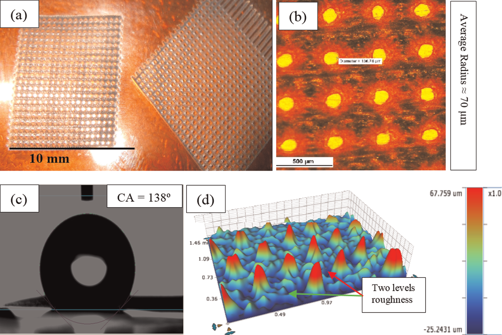
(a) Micro-pillar texturing on Kapton sheet image, (b) optical microscopy image showing a top view of the micro pillars (yellow circular boundaries), (c) contact angle of water droplet with Kapton surface and (d) 3D optical profilometer image of the micro-pillar array.
Texturing on silicon carbide (SiC)
Wang and Bai 28 conducted experiments and fabricated arrays of circular micro dimples on SiC surface and concluded that the diameter of circular dimple has significant influence on the contact angle as compared to other dimple parameters. Figure 9(a) shows circular dimples created on the surface of SiC substrate in which the diameter of the dimple is 150 µm, distance between the two dimples is 200 µm and depth is 10 µm. The process used was laser marking process with the input power of 0.3 W. Figure 9(b) shows the interaction of the water droplet with the micro-dimpled surface.
(a) Circular micro-dimple array generated on SiC surface using laser marking process and (b) contact angle with water droplet on 150-µm-diameter circular micro-dimple array. 28
Textures on metals
In general, metallic surfaces and metal oxides have high surface energy. It makes the surface hydrophilic in nature, when in contact with the liquid. To alter the surface property to hydrophobicity, polymeric modifiers (e.g. nanocoatings of polymers) are applied to form a layer of few micrometers on the top. However, such modified surfaces when subjected to a critical environment fail due to poor resistance of polymers to high temperature and abrasion. 29
In the past, several research works have been conducted in which nature-inspired metallic surfaces are generated by combining micro textures and nanostructures through different methods. These surfaces are widely employed in essential applications such as producing special surfaces (namely, anticorrosive surfaces, antifouling, antimicrobial, anti-icing and so on) and microfluidic systems, oil–water separation system, liquid transportation system and similar other areas. 30
LST process is an advanced process which can be applied for large-area texturing applications at micro or sub-micrometer level in metallic flat and cylindrical surfaces. The potential of this process in several applications such as mechanical seals, piston rings, thrust bearings and so on is explored and developed.4,31
Du et al. 32 reported production of array of micro bumps of sombrero shape having diameter in the range of 230–250 µm and height of 2–4 µm using pulsed neodymium-doped yttrium aluminum garnet (Nd:YAG) laser on bearing steel GCrl5. The bumps so generated had significantly higher hardness than that of the base metal. Vilhena et al. 33 demonstrated fabrication of array of micro pores (lubricant reservoirs) of diameter varying from 50 to 200 µm with depth of 2–10 µm using pulsed Nd:YAG laser (emitting at 1064 nm) on 100Cr6. The study was followed by performing test of sliding wear and found reduced friction when using contact pressure of 0.08 MPa and sliding speed of 0.01 m/s. The effect of micro-dimple array created by LST was found to reduce the friction on pin-on-disk machine. 34 Tribological behavior of micro-dimpled surfaces of steels and ceramics is studied,35,36 and reduction in friction under lubricated sliding conditions is reported.
Some experiments are performed on Ti6Al4V using Nd:YAG laser (FibreMark Fusion) to study the micro features generated on metallic surfaces. Textures are created by providing motion to the laser beam in linear pattern in two perpendicular directions (Figure 10). The height of the micro protrusions can be controlled by controlling the laser beam intensity. Higher intensity laser beam cuts wider area and higher depth. The schematic diagram in Figure 10 shows the cross-sectional view of the textures generated. A total of two levels of roughness are obtained by machining micro channels in two perpendicular directions.
(a) Micro-pattern array generated on Ti6Al4V and (b) schematic diagram showing a cross-sectional view of micro patterns.
Hydrophobicity on metals
There are two ways of generating hydrophobicity on metallic surfaces: (1) hydrophobic nanocoating and (2) surface texturing. A large number of researchers are currently working in the challenging areas of mimicking natural surfaces such as lotus leaf on metallic surfaces. Hydrophobic surfaces have property to repel water droplets, and during rolling of these droplets, dirt and foreign particles adhered to the surface flush out. A total of two levels of hierarchal structure (roughness) provide contact angle >110° (with water) which results in super-hydrophobicity. Surfaces having low contact angle (<65°) and high surface energy lead to hydrophilicity. 37
Potential applications of hydrophobicity
Nowadays, hydrophobicity is highly demanded on the surfaces of critical components. For example, by inducing hydrophobicity to an impeller casing and blades of a centrifugal pump, one can make the impeller last longer. The fluid being pumped by the impeller gets repelled from the metal surface which reduces fouling and enhances the durability of the metal surfaces.
Super-hydrophobic-textured metal surfaces can be used to protect airfoils and aircraft engines against the accumulation of ice during high-altitude fly, as well as to make more weather-proof infrastructures (buildings, towers and so on). The area of applications of hydrophobicity is quite wide, including power transmission lines, pipes of air conditioners and refrigerators, drag reduction, radar or telecommunication antennas and so on. Furthermore, the super-hydrophobicity also enables other highly desirable functionalities, such as anti-corrosion, anti-icing, 38 anti-biofouling, antimicrobial, low flow resistance and platelet anti-adhesion. 39
Production of hydrophobic surfaces through micro-pillar array fabrication
Tang et al. 40 produced super-hydrophobic surface on brass substrate using pulsed UV laser ablation. The volume of the material removed through laser ablation from the brass surface depends on focused laser beam spot size. The beam spot size (≈40 µm) of the laser beam governs the pitch of the quadrilateral grids produced on the substrate and results in high-density spikes as shown in Figure 11(a). The height of these spikes is ≈ 20 µm (as shown in Figure 11(b)) which depends on the intensity or power of the laser beam.Figure 11(c) shows the magnified view of a micro pillar and second level of roughness generated by ablation and resolidification of the metal.
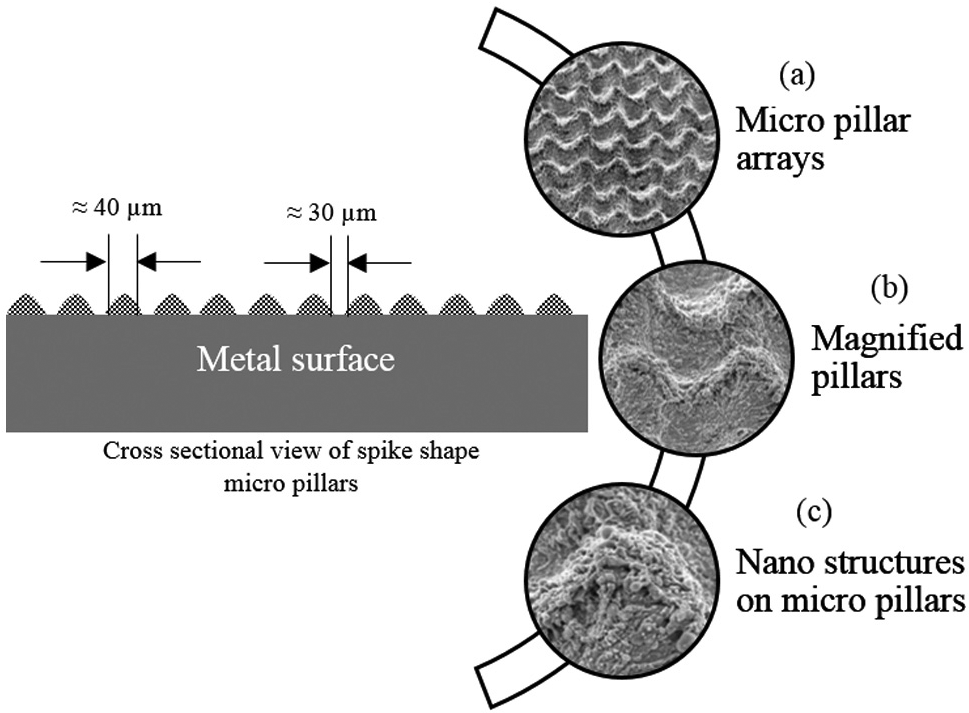
Left schematic diagram showing a cross-sectional view of spike-shaped micro- or nanostructures formed on the brass substrate: (a) array of micro pillars generated by 355-nm UV laser ablation, (b) magnified view of the same surface showing profile of the pillars and space between them and (c) nanostructures generated due to laser ablation and resolidification showing second level of roughness.
Surface roughness (Ra) varies from ≈400 nm to ≈5 µm. Meanwhile, plenty of nanostructures (200–600 nm) are also machined and scattered on the surface of the microstructures (Figure 10). Such type of manipulations on the metal surface results in water contact angle lying between 110° and 161°. Vorobyev and Guo 41 studied multifunctional metallic surfaces (platinum, titanium and brass) by generating a hierarchical nano- or microstructure with the help of femtosecond laser. Figure 12 shows the structure generated on the titanium surface. Micro-projection dimensions are height ≈ 20 µm, width ≈ 30 µm and distance between two projections ≈ 30 µm. Surface was post-examined for super-hydrophobicity and self-cleaning by spraying real dust on the surface and providing droplets of 2–3 mm diameter.
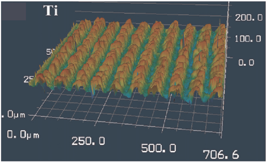
Laser microscopy image showing surface structure on titanium. 41
Del Cerro et al. 3 conducted experiments to generate erosion-resistant anti-ice surfaces with the help of ultra-short laser pulses by combining with plasma technique. It was concluded that plasma deposited hard coating reduces surface energy. Diamond-like carbon (DLC) coatings with different surface energies were applied on stainless steel surface via plasma-enhanced chemical vapor deposition (PE-CVD). Laser-machined patterns were treated with plasma-deposited hard coatings, for example, DLC, which reduced surface energy and induced erosion resistance and anti-ice surface characteristics (Figure 13).
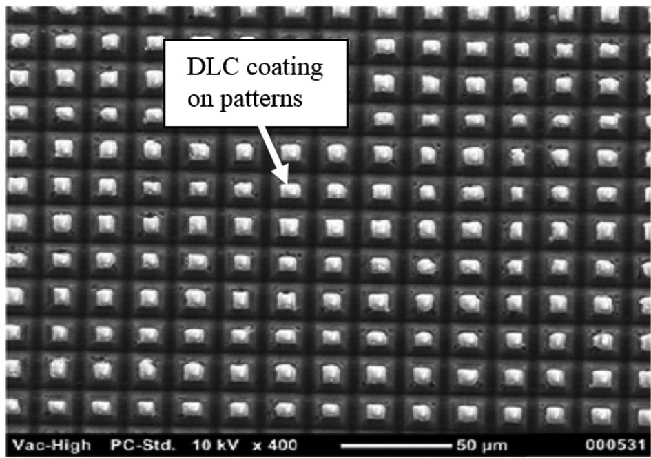
SEM image of laser-textured surface having space between pillars of 20 µm and DLC coating over the pillars. 3
Sun et al. 42 generated super-hydrophobic surfaces (water contact angle of 165°) on zinc substrate using EC processing followed by a coating with a fluorinated polymer. Micrometer-scale pits, protrusions and numerous nanometer-scale dendrite structures were found on the surface. Figure 14(a) shows SEM image of un-textured Zn surface. Figure 14(b) shows groups of micro or nano pits generated due to anodic dissolution after processing time of 1 min. Figure 14(c) shows random micro protrusions generated between two or more micro pits by the anodic dissolution. These micro protrusions work as micro pillars and generate micrometer-level surface roughness. Nanometer-level surface roughness is generated by coating the fluorinated polymer using nano-level dendrite structures (in random nature) as shown in Figure 14(d). Combination of these two levels of roughness results in a super-hydrophobic surface with water contact angle of 165.3°. Figure 14(e) shows the interaction of a droplet with the Zn surface. The spherical shape of the droplet indicates that the surface is super-hydrophobic.
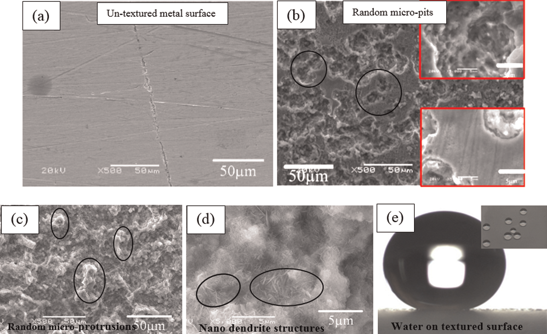
SEM images of (a) un-textured metal surface, (b) clusters of random micro or nano pits generated when machined up to 1 min, (c) micro protrusions generated due to random micro pits, (d) textured surface coated with fluorinated polymer showing nanometer-scale dendrite structures and (e) optical image of droplets on the zinc surfaces. 42
Bio-inspired textures were 19 fabricated by generating hierarchal micro-nano pillars of different geometries. It is reported that ice adhesion on the surface having hierarchical micro-nano pillars was lesser as compared to the surface having micro pillars only. Figure 15(a) shows the micro-pillar-based surface textures generated on (100) oriented p-type silicon wafer by lithography and deep reactive etching. Figure 15(b) shows the nano pillars fabricated on the micro pillars, and Figure 15(c) shows the interaction of a droplet with textured surface emphasizing on horizontal and vertical contacts. These hierarchical structures consisting of micro-nano pillars are fabricated by combining deep reactive etching and galvanic etching process.
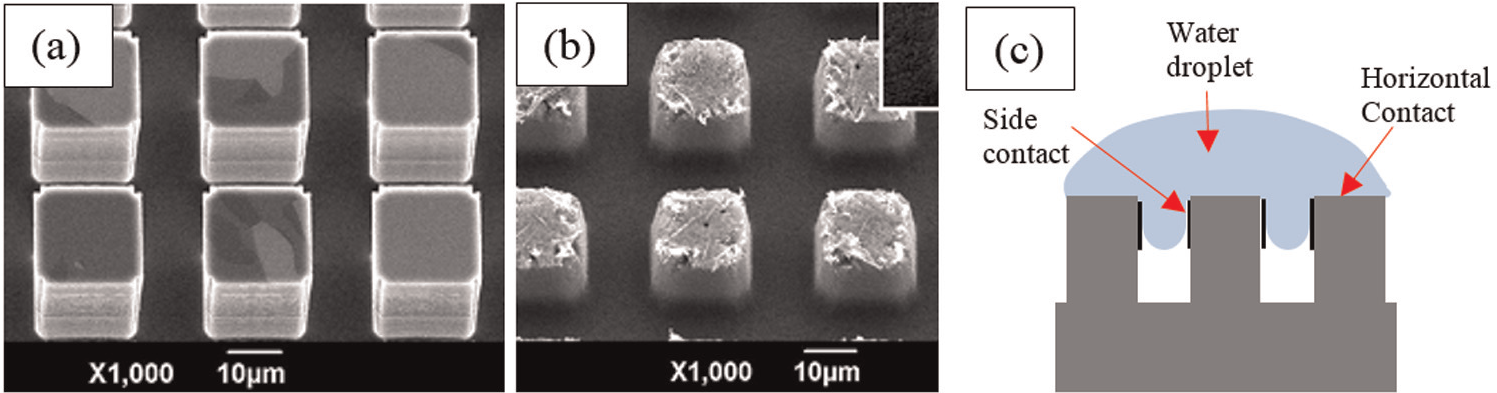
SEM image of the textured surface: (a) only micro-pillar array, (b) hierarchical micro-nano pillar array and (c) contact area model of droplet interaction with the micro pillars where vertical contact area and horizontal contact area are highlighted. 19
At-a-glance micro or nano processes of texturing
From the above literature survey, the following points can be enlisted:
LST is a promising technology which can produce well-defined repeatable micro features on metals as well as nonmetals. However, use of laser machining for generation of micro or nano features or structures at large scale is not economically viable. Furthermore, LST process is a thermal energy–based machining process; hence, micro- or nanostructures get distorted or even melted out. Indeed, LST is a good option for polymer machining, but it is difficult to machine metallic surfaces especially on curved surfaces.
Electric discharge (ED) texturing is also a thermal energy–based process; hence, due to high temperature, mechanical properties of the machined surface get changed and micro or nano features may get distorted or vaporized. 43 Other problems associated with ED texturing are heat-affected zone, recast layer, thermal residual stresses, micro cracks and so on.
Processes such as nanocasting and lithography are not suitable for large-scale production since multiple steps are involved, namely, insulation, mask generation and machining.
Electron beam machining (EBM) and focused ion beam milling (FIBM) are the excellent processes known for working at micro- or nanometer level.44,45 But for large-area surface texturing, they demand large amount of time and resources.
Chemical texturing is a process which can be utilized for very large-area texturing on some specific materials. For example, sodium hydroxide–sodium hypochlorite (NaOH–NaOCl) can etch multicrystalline silicon wafer without grain boundary (GB) delineation, and it can produce texture on 150 mm × 150 mm area. 46 But the process does not have an efficient control over the variables so that a large variety of the parts can be textured. The process is very complex and requires vast knowledge of chemical engineering because each metal or alloy requires a specific etchant(s).
The current review discusses several studies of EC micro-texturing process such as jet electrochemical micromachining (ECMM), through-mask electrochemical micromachining (TMEMM) 47 and so on. These processes are under development stage in context of improvising the accuracy of machined features such as micro dimples and micro patterns. Such processes control EC dissolution of the targeted zone with the help of a mask. Although once the mask is accurately designed and fabricated, it can be used many times for generating textures at large scale. Generation of these masks requires another process such as laser machining and/or lithography. Thus, it makes the texturing process again a multiple-step process.
Production of micro pillars (or micro protrusions) at large scale on metallic surfaces to alter their surface energy is also extremely difficult and uneconomical using the processes such as TMEMM, laser beam micromachining, electron beam micromachining and so on.
It can be concluded from the above discussion that there is a need to develop a single-step technique for large-area surface texturing on metallic surfaces for altering their physical properties. The method should be economically viable and technically feasible for mass production. This method should not alter mechanical properties of the textured surface.
ECMM process is a process in which metal removal takes place at atomic or molecular level. A specific single-step EC micro-texturing method is desirable (without using a mask) to reduce the number of steps of the process. Initial ideas for a controlled hierarchical two levels of roughness production methods are also presented in this study.
From the above merits and demerits of different micro-texturing processes, it can be concluded that the laser beam micro or nano texturing and EC micro texturing are the feasible and economically viable processes for micro texturing on flat and curved metallic surfaces. Hence, these two processes have been further examined in Table 3 to explore their capabilities so that an appropriate process can be selected for a given task.
Comparison of two techniques of micro texturing on metallic surfaces.
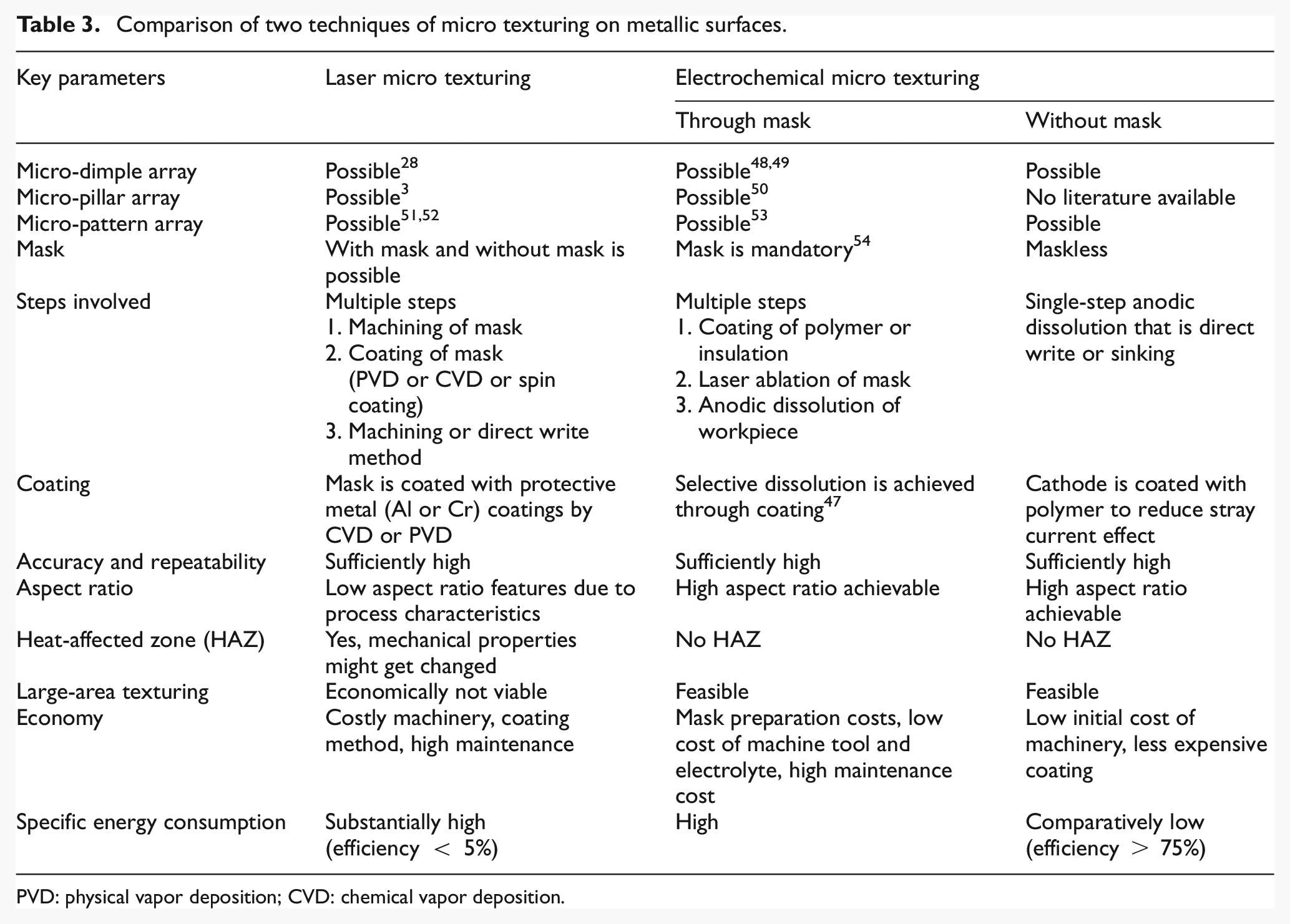
PVD: physical vapor deposition; CVD: chemical vapor deposition.
After going through Table 3, it can be concluded that there is a merit in exploring and developing a process of single-step EC micro texturing for the flat and curved metallic surfaces. This article presents some overview of the literature survey and some original research work on the flat and curved surfaces.
EC micro texturing
ECMM is an anodic dissolution process in which metal removal takes place atom by atom from the anode (i.e. workpiece). Pre-patterned tools are used as a cathode. Because of the absence of direct contact between the tool and the workpiece, there is no mechanical cutting force acting on the workpiece, and minimal heat is generated due to EC reaction and mechanical action. Hence, practically, there are no thermal (residual) stresses and surface defects in the machined workpiece. In addition, material removal rate (MRR) is much higher as compared to other advanced machining processes. Such capabilities of the ECMM process make it suitable process to achieve micro- or nanostructures on metallic surfaces. 55
ECMM has high potential on account of versatility of its applications. It is a promising and economically viable machining process for micromanufacturing industries for fabrication of micro textures and micro features on metallic surfaces. From the last few decades, large-area texturing has become unavoidable, and extensive research work is going on in this domain. Indeed, TMEMM, lithography, micro- or nanocasting and so on are the existing methods which involve multiple steps for generation of surface textures. For large-area applications, it is desirable to have a single-step process in place of multiple-step process to make it highly productive and economically viable process. The work in this direction is in progress to use a single-step maskless EC micro-texturing process with a pre-patterned micro tool. Selective EC micro dissolution will be achieved by controlling the stray current effect 56 using a thin nonconducting layer coating on the cathode surface.
Major input parameters influencing the dissolution of metal to create micro textures are type of electrolyte used, electrolyte concentration, size and shape of the tool, current density and so on. The enhancements of ECMM accuracy and performance efficiency are the current areas of research. The major problem of any ECMM process is optimization of process parameters which affect the process output, namely, accuracy, performance and surface roughness of the machined texture.
The advantages of electrochemical machining (ECM) are now being realized in different industries, and the process is being used in extensive ways for shaping of knitting machine cam, master die preparation, drilling of kidney-shaped slots, turning of metal bars 57 and so on. In the present scenario, there is a tremendous force from the market toward miniaturization, that is, the reduction of the dimensions of any engineering product. Thus, miniaturization has extensive applications in various industries, namely, electronic, semiconductor, aerospace, medicine, optical, biomedical, automotive, air conditioning and tribological. Many times micro features are required by ultra-precision machinery parts for the fabrication of microproducts such as inertia sensor (for air bag deployment systems in automobiles), read–write heads (in computer storage systems), nozzles of inkjet printers, biomedical filters, micro robots, micro cars, microscale devices such as micro-heat exchanger, microscale chemical reactor, micro pump, micro-pin fins, micro-heat pipe, fuel injectors58–60 and so on.
All these micro components require micro features such as micro cavity, micro groove, micro hole, micro filter, micro channel, micro pillar, micro dimple and so on. These micro 3D shapes are to be machined on hard-to-machine materials such as titanium alloys, stainless steel, nickel, copper alloys and superalloys such as Hastelloy, Inconel (e.g. IN100, IN600 and IN713), Waspaloy, Rene alloys and so on. For surface texturing, specific types of features should be replicated repeatedly (with high accuracy and repeatability) to make an array out of it. Thus, it is very important to understand the generation of these micro features and achieve a great control over the fabrication processes involved.
Above narrated practices are difficult to perform by traditional methods such as turning, milling, shaping and so on due to the limitations of the design, high tool wear rate, low precision and accuracy, high surface roughness and so on. Performance of all these activities in some advanced machining processes such as EBM, FIBM, lithography and laser beam machining, abrasive water jet machining (AWJM) and ED texturing are highly challenging, and they are cost-ineffective to produce micro texturing at large scale.
Types of EC micro texturing
Creation of the designed micro features in large number on a surface is called texturing of a surface. Through such texturing, one can develop an engineered surface with the desired uniform surface roughness which will help in the control of friction characteristics, contact angle, wear of the surface and so on. If one can produce engineered surfaces with the desired surface roughness, then many problems associated with wear and tear of the moving parts can be solved.
Newer promising engineering materials are emerging through material science and engineering research. These materials are required by nuclear, aerospace, defense and biomedical engineering industries. These materials have high strength-to-weight ratio. But machining of hard-to-machine materials at microscale is very cumbersome and expensive. ECM process is the process in which machining efficiency is independent of mechanical properties of the workpiece.
In order to fulfill the demands of the industries, advanced machining techniques are evolving rapidly for machining of hard-to-machine materials. For example, wire ECM is an advancement in this domain for improvement in machining proficiency to machine high aspect ratio micro features and miniaturized parts. Ultrasonic vibration–assisted electrode in ECMM results in better surface finish generated during micromachining. 61 Table 4 shows the methods to create micro features using various versions of anodic dissolution. After creation of such features on very hard materials, they can be used as forming dies for a large-scale (or mass) production.
Recent advancements in electrochemical micromachining.
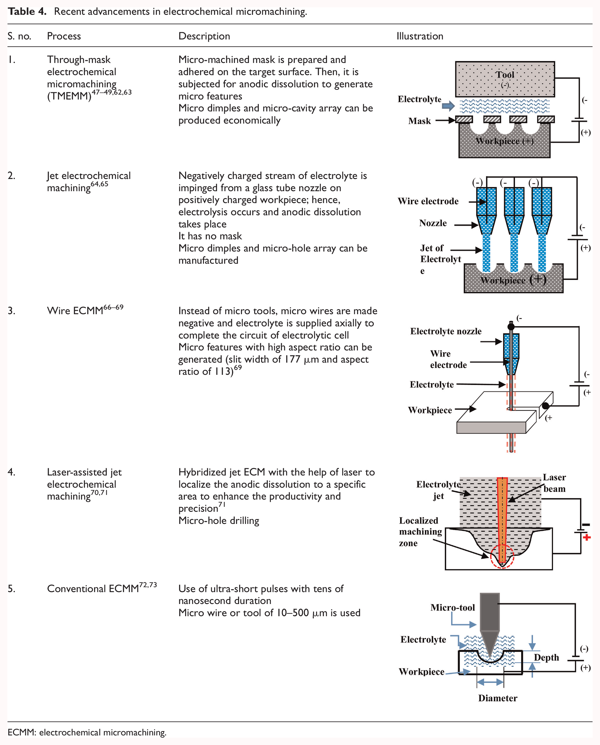
ECMM: electrochemical micromachining.
In jet ECMM, electrolyte jet of a few micrometer dimension and of different shape is used as a tool to generate micro features. Experimental findings have been reported showing the effects of applied voltage, capillary outside diameter, feed rate, electrolyte concentration and inlet electrolyte pressure on soundness of micro holes. 64 Complicated structures such as array of micro dimples, micro channels and micro grooves are made by this technique with high surface finish. 74 In the wire ECMM, novel techniques of enhancing mass transport, electrolyte flushing and so on have been proposed by incorporating axial electrolyte flow, traveling wire (tool) and vibrating the wire (tool). It has been reported that machining process acceptability has been enhanced by achieving better stability in machining, productivity and surface finish.67,68 Laser-assisted jet ECMM has shown that there is a significant enhancement in MRRs of hard-to-machine materials (Hastelloy, titanium alloy and stainless steel) due to focused EC dissolution with assistance of laser beam. There is an evidence of improvement in the shape and surface finish of the machined feature using laser beam in jet ECMM (of the order of 20%). 70
Schuster et al. 72 applied ultra-short voltage pulses between a tool electrode and workpiece in EC environment for 3D machining. The principle is based on the finite time constant for double-layer charging, which varies linearly with the local separation between the electrodes. Figure 16 shows a schematic diagram of 3D shape generation by moving a micro tool in a square path followed by a smaller rectangular path (marked with arrows).
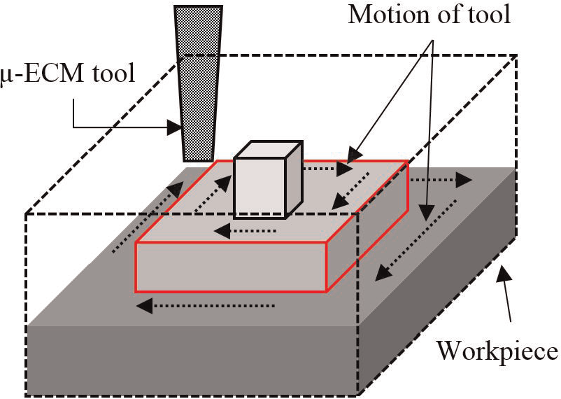
Small prism (micro pillars) fabrication using ECMM by moving a tool in two square paths in two levels to obtain a 3D structure. 72
Generation of such type of 3D features at large scale for surface texturing is very tedious by this method. From economic viability point of view, it will not be feasible to make an array of micro tools having a diameter of 10–50 µm. Ghoshal and Bhattacharyya 75 proposed a study of micro-EC sinking and milling process. A 50-µm-thick plate of stainless steel (SS-304) was machined with 8-µm tool. It is concluded that least overcut was observed in the proposed sinking and milling operations with 5 MHz pulse frequency and 0.2 M (H2SO4) electrolyte concentration.
Qu et al. 49 proposed an application of surface textures to improve the tribological performance of various mechanical components by generating arrays of micro dimples on the internal cylindrical surfaces, using ECMM. Dry-film photoresist was used as a mask.
Cho et al. 53 proposed a selective EC dissolution process (Figure 17) using laser masking for generating micro patterns on the cylindrical surfaces of stainless steel shafts. Figure 17 (left) shows the SEM images of micro-textured surface of a cylindrical bar at 35× and 150×. Micro textures are created by machining ≈100-µm-wide micro channels in jig-jag pattern. The investigation reveals that the micro patterns are produced by a series of processes of laser masking, EC etching and ultrasonic vibration cleaning. Factors causing nonuniformity are beam diameter, incident angle of laser beam and field distortion errors. These factors could be compensated via continuous line scanning of laser beam on the rotating workpiece. Figure 17(a) shows the first step in which workpiece is masked, and patterns are machined using laser beam. In the second step, cathode (tool) is brought near the masked workpiece and allowed for EC dissolution (as shown in Figure 17(b)). In the third step, the machined surface is ultrasonically cleaned and mask is removed as shown in Figure 17(c).
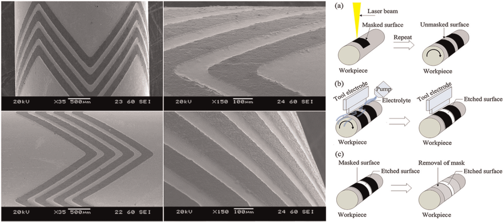
Micro patterns on cylindrical surface (left) and three-step process employed to generate the patterns. 53
Kern et al. 50 presented experimental investigations of different micro-feature fabrication using TMEMM. Patterned masks are used to manufacture different textures on the titanium surface using TMEMM process. Micro dimples (of ≈70–150 µm) shown in Figure 18(a) are fabricated by providing a mask of SU-8 on the metal surface. The mask was patterned by electron beam lithography. The 3D shapes shown in Figure 18(b) are generated by anodizing the titanium surface at 150 V in 0.5 M H2SO4 + 0.5 M H3PO4. Square-shaped pillars (of ~40 µm) shown in Figure 18(c) are generated by machining micro channels in two perpendicular directions using fraction of a mask.
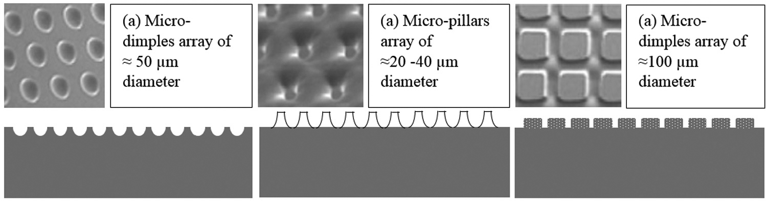
(a) Ti surfaces with well-defined hemispherical cavities by TMEMM via maskless UV patterned SU-8, (b) through-mask anodized Ti surfaces (150 V in 0.5 M H2SO4 + 0.5 M H3PO4) and (c) SEM micrographs of square micro pillars.
Micro texturing using micro dimples
Micro-dimple array plays an important role in decreasing coefficient of friction between the two surfaces having relative motion. In an internal combustion engine, friction loss is a major factor which influences the fuel economy and performance of the vehicle. 5 In a compression–ignition engine, there are 20%–30% of friction losses in the piston–cylinder system. A large part of it is attributed to the piston rings. Lubrication between the surface of piston ring and cylinder can be increased by providing micro-dimple texture on the surface of piston ring, which would work as micro reservoir for the lubricant, and it would reduce friction in a piston–cylinder system. In addition, such micro-dimple array results in substantial enhancement in load capacity and wear resistance of other mechanical components which undergo sliding motion. 4
Pettersson and Jacobson 76 researched the influence of textures on physical vapor deposition (PVD) coated TiN and DLC surfaces and reported that the use of high-precision anisotropically etched silicon surface as a substrate minimizes the influence of coarse edges and other unintended topographical features. Wakuda et al. 36 elaborated one of the presumed effects of surface texturing under boundary lubrication conditions. It is concluded that micro dimples act as lubricant reservoirs and play a role in promoting the retention of a lubricating film which reduces the friction coefficient. They also concluded that as compared to a lapped smooth surface without texturing, some samples showed a significant reduction in friction coefficient from 0.12 to 0.10. Byun et al. 77 fabricated micro dimples of 300 µm on AISI 440 C sample with the help of ECMM by employing microsecond pulse (direct current) DC power supply and presented a comparative experimental study of friction performance behavior between the textured and nontextured surfaces on tribometer and illustrated the reduction in coefficient of friction from 0.12 to 0.04. ECMM with microsecond pulses was applied in order to fabricate a micro-dimple pattern.
TMEMM was performed by Datta 62 using a pulsating voltage (current), which provides a better control over the nozzle fabrication process. State of the art of thin-film patterning (texturing) using TMEMM is also reported by Datta et al. 63 They concluded that TMEMM is capable to produce micro features over a large surface area. The effect of convective mass transport in the electrolyte and current distribution over the workpiece on the surface finish and shape evolution is presented. In micromachining, the electrode surface area is in few tens of square micrometer which leads to high instantaneous current density. Hence, it is advisable to employ pulsating current while maintaining low average current which is desirable for thin-film processing. Electrolyte used in this study was 3 M sodium nitrate (NaNO3) containing 100 ppm of FC-98 (3M Company, St Paul, MN), a nonfoaming surfactant. These experiments also included the study of the influence of glycerol on the anodic polarization behavior of stainless steel in chloride solution. Glycerol was added to increase the viscosity of the electrolyte and enhance surface smoothness. The surfactant potassium perfluorobutanesulfonate (FC-98) was used to ensure uniform wetting of the entire surface.
Jet ECMM was employed by Lu and Leng 78 to produce micro hole of ≈450 µm in diameter (as shown in Figure 19(a)) and have an aspect ratio of over 1.3 on titanium specimens. Machining was carried out for 2 min with the voltage of 200 V and average current of 45 mA. It is reported in the study that while machining below 100 V, EC dissolution is near to zero, and if machined above 250 V, electric sparks are generated due to high current. As the current density increases, stray current effect also increases which results in significantly poor surface finish. Pitting near to the drilled holes was also reported as shown in Figure 19(b). Figure 19(c) shows an optical image of micro holes produced on Ti6Al4V plate after 15 min of etching at 0.1 A current.
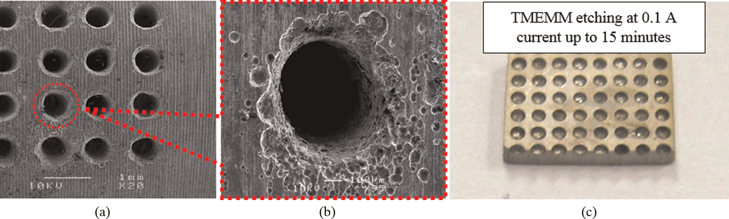
SEM micrographs of (a) micro-hole array produced on the Ti6Al4V cylinder surface using jet ECMM, (b) pitting (micro craters) due to machining over 250 V and (c) optical graph of micro dimples produced on Ti6Al4V plate after 15-min etching at 0.1 A current. 78
Landolt et al. 79 demonstrated fabrication of multiple-level structure with the combination of TMEMM and controlled anodic oxidation on nonplanar surfaces. Figure 20(a) shows the highly dense micro dimples of 30 µm diameter created by TMEMM process. Figure 20(b) shows nanopores generated inside the micro dimples by anodic oxidation. Anodic oxidation was carried out in 2 M H3PO4 by sweeping the potential at 20 V/s to a final value of 175 V. This validated several potentials of the process for biomedical engineering, MEMS and micromechanic applications. High-resolution features of nanometer scale can be repeatedly produced by the combination of these two processes (TMEMM and anodic oxidation in H3PO4).
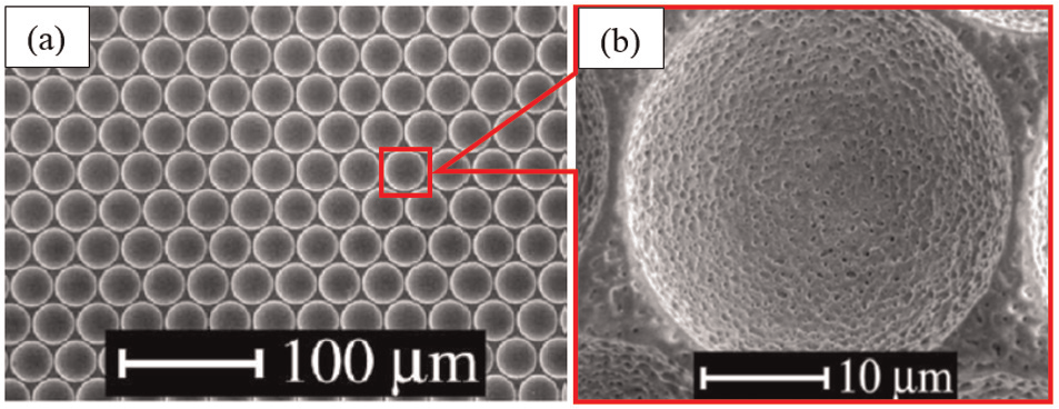
(a) Micro dimples of 30 µm on titanium produced by TMEMM process and (b) nanopores generated inside micro dimples by anodic oxidation. 79
Effect of current density and mass transport on surface finish in ECMM
The surface finish reported in ECM is 0.1 µm, 57 and with an ECMM setup, the roughness of ≈500 nm can be achieved. Kawanaka et al. 80 presented an experimental investigation of jet ECMM (illustration is tabulated in Table 4) and claimed that higher current density results in a mirror-like surface, while lower current density realizes significantly rough and complicated structures which are difficult to obtain with other machining processes. Figure 21 proves that when current density increases from 25 to 187 A/cm2, roughness value decreases significantly, and mirror-like surface is obtained when current density is above 100 A/cm2.
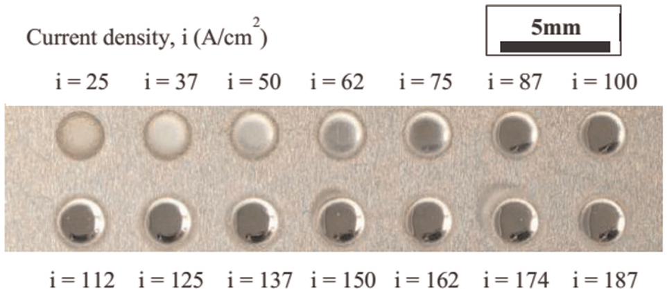
Dimples machined on stainless steel (SUS304) with increasing current density. 80
The surface roughness is governed by current density, and it is affected by grain orientation, GBs, dislocations and small inclusions. The reason for decreasing Ra value of the machined surface at higher current density can be understood through Figure 22. However, for a given set of machining conditions including tool and workpiece material, there is always a critical surface roughness value.
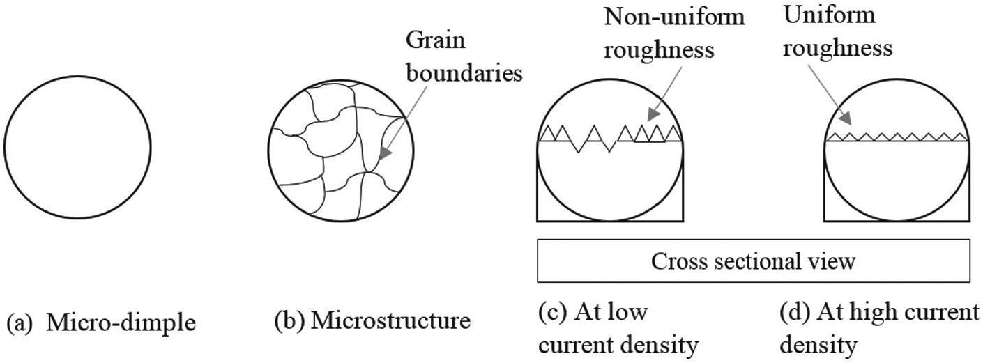
(a) Top view of the micro dimple machined; (b) grain boundaries available at the metal surface; (c) nonuniform surface roughness at low current density, when anodic dissolution is more at GB and (d) better machined surface at high current density, when anodic dissolution is uniform.
The resistance for EC dissolution at GBs is comparatively low due to nonuniformity between the joint of two or more crystals; hence, the GBs are attacked first (Figure 22(b)). When the current density is very low, material near to the GBs gets dissolved, and a rough surface is obtained. (Figure 22(c)). As the current density increases, the resistance at GBs gets dominated, and metal is removed uniformly from the surface and leads to a mirror-like surface (Figure 22(d)).
When inhomogeneous materials or alloys are machined at low current densities, one component may get removed preferentially because different constituents of the anode material may have significantly different electrode potentials which results in poor surface finish. 57 Landolt et al. 79 explained the relation of surface roughness through the concept of mass transport. Mass transport plays a dominant role in EC dissolution processes at micro-level texturing because it can affect current distribution on a macroscopic scale and a microscopic scale. Since protrusions available on the surface have higher current densities compared to the flat surface, it results in surface smoothening, which is also called leveling effect. Experimental investigations have been carried out to find out the relationship between current density and surface finish as discussed in section “Micro-dimple array texturing on flat metallic surface.”
Experimental investigations
Micro-dimple array texturing on flat metallic surface
Experiments are conducted on a tabletop multi-process micro-machine tool (Hyper-10) of Synergy nano systems. The working setup is shown in Figure 23(a) and (b).
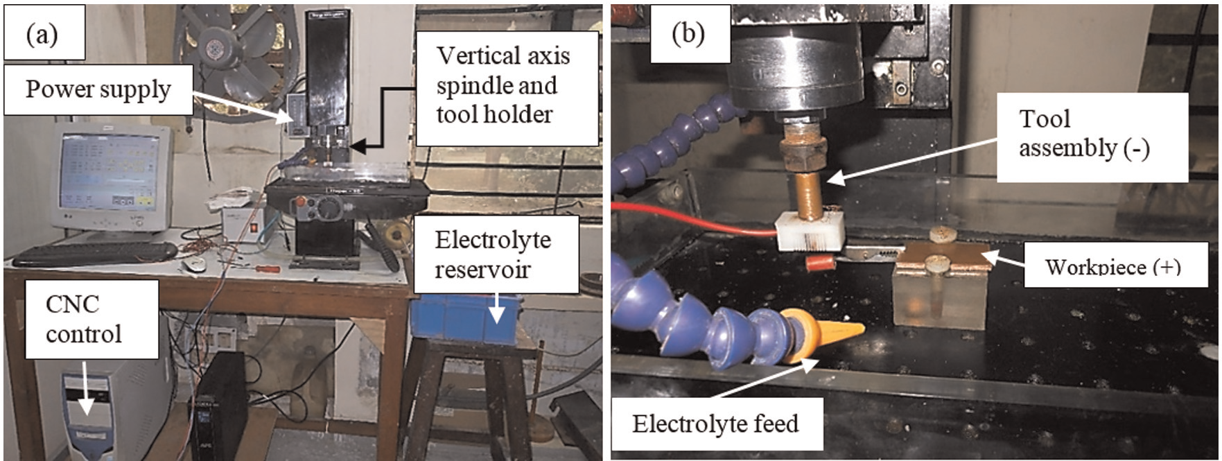
(a) Present experimental setup and (b) machining zone showing tool assembly held on machine spindle.
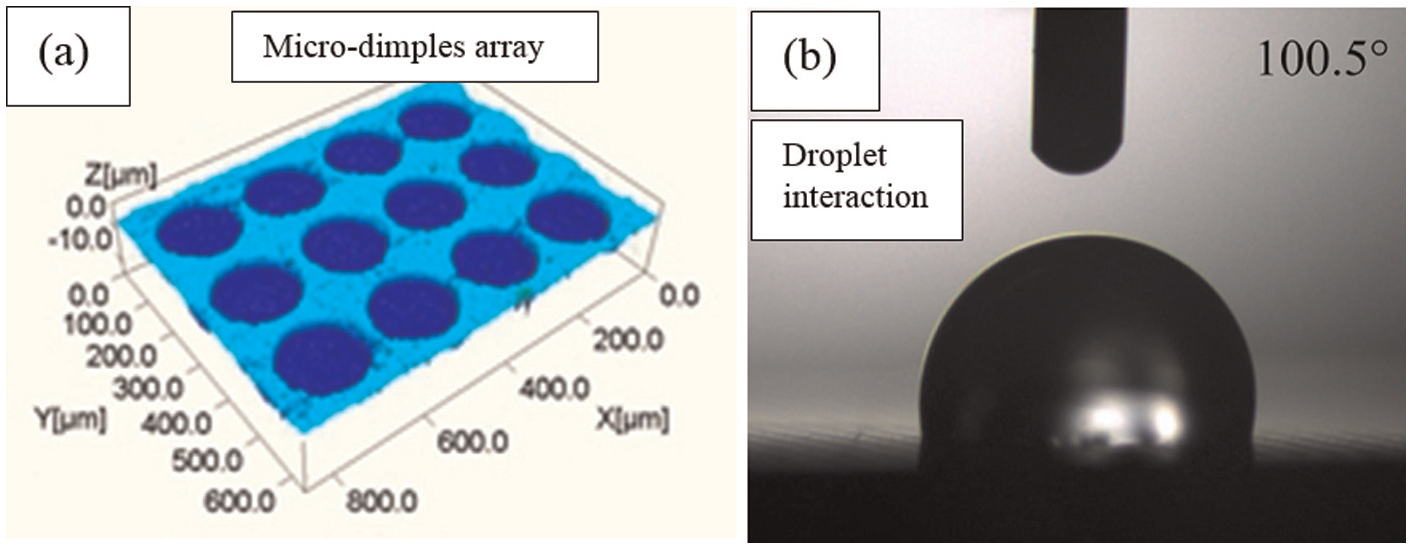
A schematic diagram shown in Figure 24(a) shows a simple experimental strategy for generation of micro dimples on flat surfaces. A tool with 300 µm diameter at the tip is held on the machine spindle. Less toxic electrolyte with 0.5 M concentration is pumped in the inter electrode gap of 100 µm with velocity of 5 m/s. Input supply voltage is varied from 10 to 20 V, and consequently, current value varies from 1 to 3 A. During creating micro-dimple array, machining time was kept constant as 20 s.
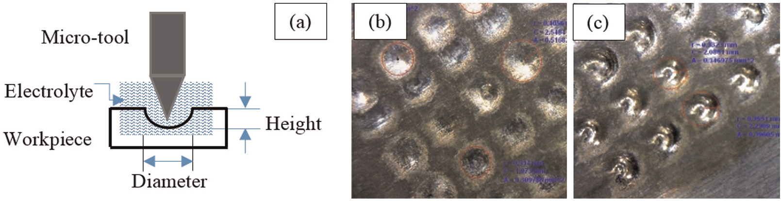
(a) Schematic diagram of the ECMM direct write method, (b) EC micro-machined dimple array of 600 µm at 10 V and (c) EC micro-machined dimple array of 600 µm at 20V.
Relation of current density with surface finish of machined surface can be understood from Figure 24(b) and (c). Micro dimples of 600 µm diameter are machined at 10 V. The dimples obtained are rough because the GBs get machined first, and some part remains un-machined (Figure 24(b)), which is a rough surface. When the applied voltage is increased to 20 V, due to very high current density, machining rate remains uniform at GBs as well as on grains. It leads to low roughness (as explained in case of Figure 22) and mirror-like finish is obtained (Figure 24(c)).
Micro-dimple array on hypodermic needle
Significant efforts have been made in the past for developing low-invasive medical treatments. The development of mosquito proboscis–based needles for reducing pain while insertion, biodegradable micro needles which dissolve along with the drug under the skin and so on represents some of the latest research being carried out in this arena. 81 Ultrasound-guided foam sclerotherapy, in which a doctor injects sclerosant foam along the length of varicose vein and a patient feels a lot of pain. In this treatment, same hypodermic needle is injected multiple times on the same patient which results discomfort and pain to the patient. 82 Oka et al. 83 demonstrated fabrication of micro needles with jagged shape like that of a mosquito. It was made of silicon dioxide (SiO2), and jagged features were created by depositing poly-Si on the surface of hollow needle. To analyze the effect of surface textures on the insertion force, it is very essential to understand the mechanism of force measurement. Insertion force measurement analysis of a needle can be performed by mounting the needle on a motor-driven spindle and inserting it on human skin–like polymer. The polymer is mounted on a load cell, which consists of a piezoelectric sensor.82,84 Above narrated studies have shown that micro textures produced on the hypodermic needles reduce the insertion force by reducing the coefficient of friction between the insertion media and textured needle.
TMEMM involves the machining of a mask, which itself increases the complexity, overall machining time and manufacturing cost. However, surface of needles can be improved by producing arrays of micro dimples on it through ECMM without using mask. It reduces the number of steps of the process and hence the cost of machining. Some experiments have been conducted to explore the feasibility and to study surface roughness and other characteristics of the dimples so produced. The process can be understood with the help of a schematic diagram shown in Figure 24(a). A micro tool of 250 µm is kept at a distance of 100 µm from the workpiece. Figure 25(b) and (c) shows the dimples created on the surface of a hypodermic needle (Figure 25(a)) and its magnified view through an optical microscopy.
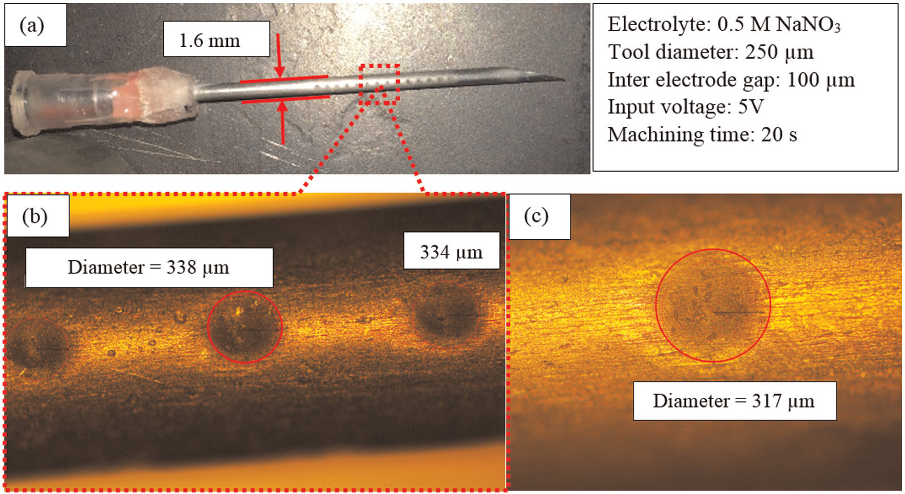
(a) Micro dimples generated on hypodermic needle of 1.6 mm diameter, (b) optical microscopic view showing micro dimples (≈335 µm diameter) on the needle surface and (c) magnified image of micro dimple of 317 µm diameter.
The geometric and dimensional parameters of the profile of micro dimples are observed on 3D optical profilometer as shown in Figure 26. It can be seen that the maximum depth of dimple shown is 19.1 µm and diameter is ≈320 µm.
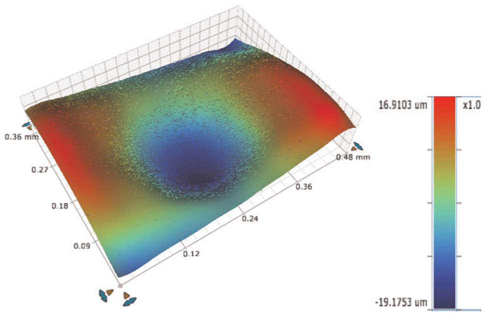
3D optical profilometer image showing the profile of a dimple and its dimensions.
Profile inaccuracy in dimples
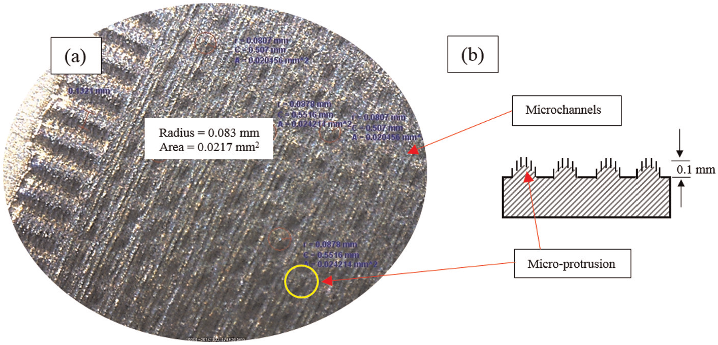
During pilot experiments, it was found that when the electrolyte was supplied from the side of the tool, the profile of the dimple generated was inaccurate because of the presence of a micro protrusion inside the dimple (as shown in Figure 27), that is, un-machined part. Figure 27(a) shows the inaccuracy generated during one-sided electrolyte flow machining with the help of optical microscope (OM) image. The diameter of the dimple is 374.04 µm. Figure 27(b) shows 3D optical profilometer image of the micro protrusion. Figure 27(c) shows measurement of diameter and depth of the dimple and profile of micro protrusion left un-machined. The depth of the dimple obtained is 107.9 µm.
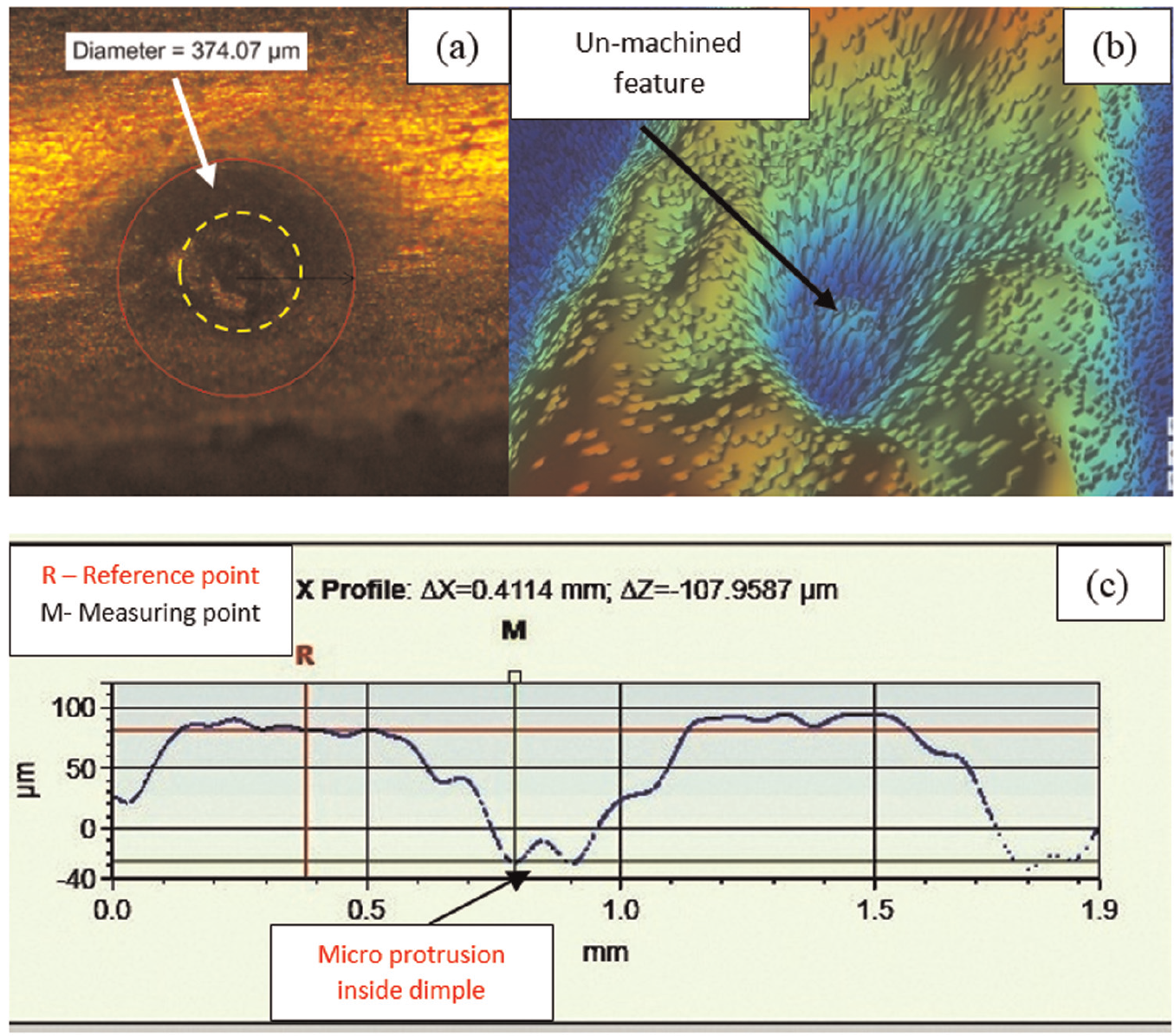
(a) OM image showing un-machined part inside the dimple; (b) 3D optical profilometer image of the micro protrusion left un-machined and (c) measurement of dimple depth in 3D optical microscope image, that is, Δz = 107.9 µm, and profile of micro protrusion at the bottom of the dimple.
It was found through the experimental investigations that the flow of electrolyte is a critical input parameter, resulting in this type of inaccuracy in the profile of the micro dimple. When electrolyte is supplied from the side of the tool (as shown in Figure 28(a)), the flow is obstructed by the tip of micro tool. Thus, the electrolyte flow is less behind the tool, resulting in improper anodic dissolution in that zone. This error disappears by making electrolyte flow through the hole in the nozzle along the axis of the tool as shown in Figure 28(b). When the electrolyte is supplied from the axis of the tool, sludge removal gets enhanced, and there is no part left un-machined. 55
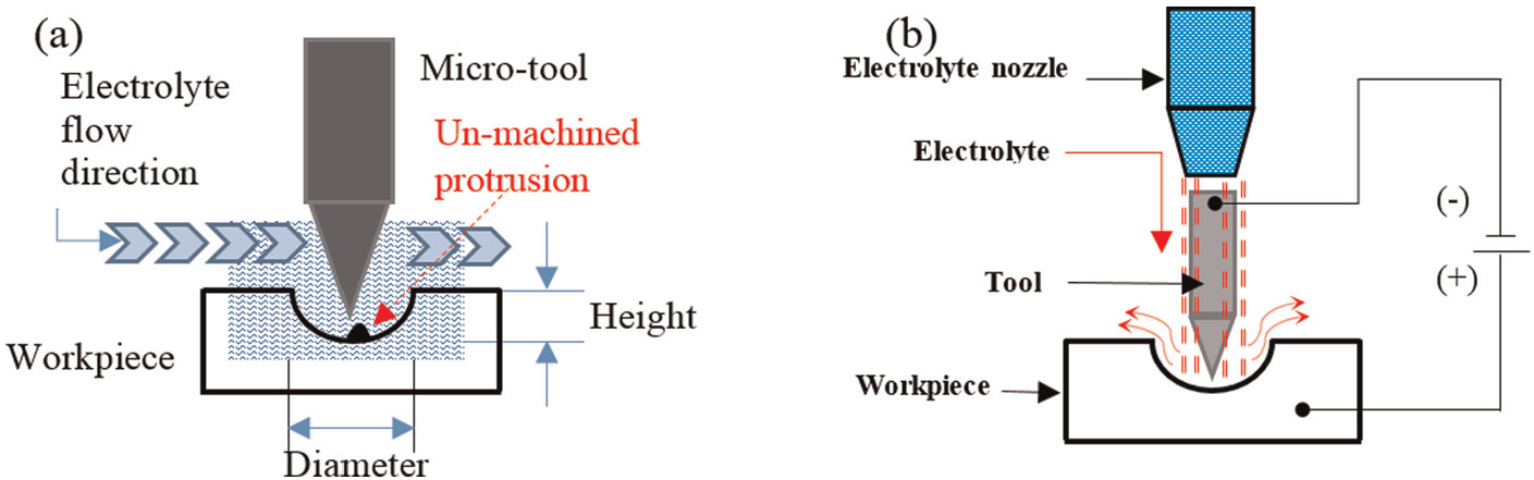
(a) Schematic diagram showing one-sided electrolyte flow and left un-machined protrusion and (b) modified axial electrolyte feed system.
Micro-pillar texturing
A major shortcoming of an ECMM process is the occurrence of overcut due to stray current effect. The effect of this weakness can be reduced using micro wire tools (or pre-patterned tools) of the required structure along with electrically nonconducting coating on its selected surface. Acrylic chips are melted in chloroform and stirred for few minutes. The tool is mounted on numerically controlled (computer numerical control (CNC)) vertical axis drive system and dipped precisely into the molten solution of polymer up to the desired depth. Instead of continuous pulse, low-voltage short pulses are used for the controlled anodic dissolution. Less toxic and less aggressive electrolyte (0.5 M NaNO3) is used during the experiments.
EC texturing by wire mesh
A pre-patterned tool is fabricated, and a nonconducting polymer is coated on the half surface area as shown in Figure 29. Micro protrusions have been generated with the help of EC sinking operation in the following.
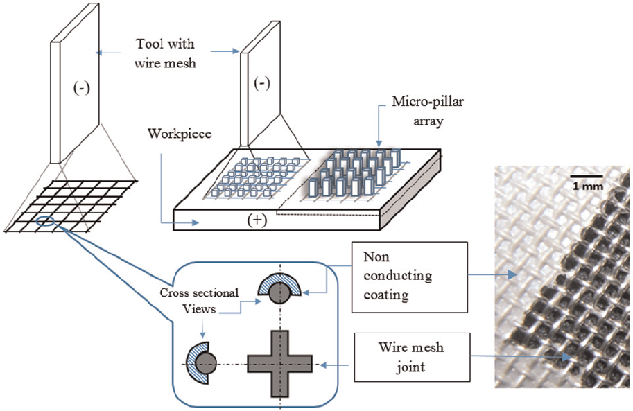
Schematic diagram showing methodology of EC texturing using coated wire mesh cathode.
For reduction of stray current effect, the tool is coated on its upper half surface (see photograph in Figure 29). Figure 29 also illustrates the magnified view (in window) of an element of the wire mesh tool with coating. It can be coated by a polymer or a hydrophobic nanocoating to ensure that there is no direct electrical contact between the metal under coated area and electrolyte. This coating can be applied either by dip coating or spray coating. As a result, a confined EC dissolution can be achieved by restricting the reactions into the conducting zone only, and hence, overcut can be minimized. Due to this control over the metal surface, wherever there is conducting tool in the machining zone, the material from the workpiece will be dissolved, and in the space between these conducting wires, pillar-like structure will be left un-machined. Figure 30(a) shows experiment of EC wire mesh sinking. Wire mesh tool is first dipped coated in acrylic and chloroform solution from one side. It is very important to hold the wire mesh in the machine spindle with high precision and accuracy during ECMM operation; otherwise, short circuit might take place. A special wire mesh holder is designed and manufactured by 3D printing (as shown in Figure 30(a)) and employed during the machining. Figure 30(b) shows the textured surface (consist of protrusions of 500 µm in diameter) obtained after wire mesh tool sinking operation.
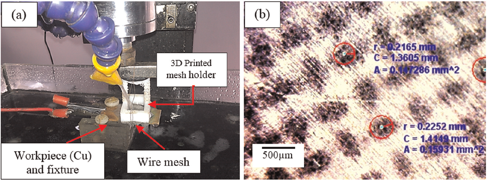
(a) Experimental setup of wire mesh EC texturing and (b) textured surface of mild steel showing protrusions of 400–500 µm diameter.
Micro texturing through composite tool
Figure 31 shows the methodology of experiments and results of EC micro texturing through composite tool sinking. A number of multiple thin metallic sheets are clubbed together to make a composite tool for EC sinking operation (Figure 31(a)). The picture in Figure 31(b) shows the experimental texturing zone of EC texturing setup. With this composite tool, multiple channels are created in one direction (Figure 31(c)) as shown in step 1. The space between the two channels is governed during the tool design and motion of tool. Furthermore, space between two channels is again machined by moving the tool assembly by 200 µm as shown in Figure 31(c) (step 2, black dashed lines show moved distance by the composite tool). In the third step, the tool is rotated by 90° (it can be by other angle also) and then the channels are created at 90° to the channels created in the earlier parts. Figure 31(d) shows micro-channels created in one direction with the help of composite tool design and moving the workpiece table. The intersection of these two sets of channels results in the creation of protrusions of the discussed shape and size as shown in Figure 31(e).
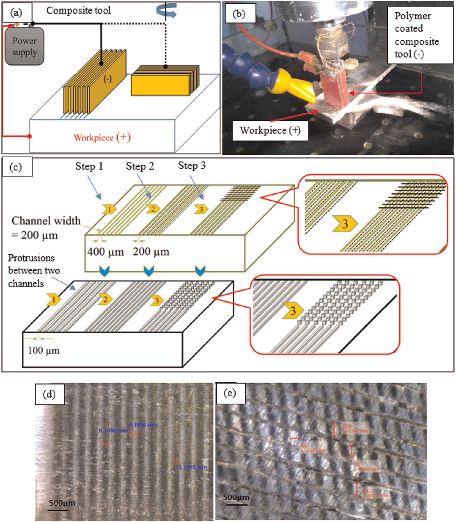
Micro-pillar fabrication using a composite tool sinking: (a) schematic diagram showing the organization of composite tool and (b) image of real experimental arrangement of the same, (c) micro-channel to micro-pillar strategy in three steps and (d) channels and textures generated on mild steel flat surface. (d) Micro channels created during the second step of the operation and (e) micro pillars created in the third step (by rotating the tool assembly by 90°).
From the above discussion, it is concluded that the ECM process can be explored for the production of hydrophobic surfaces which require two levels of surface roughness. Primary projections range from a few tens to a few hundreds of micrometer dimensions which have been reported in this article. For nano hair or projections, two strategies are being planned: first, using primary surface roughness texture as nano hairs and, second, using a tool having nano projections produced by focused ion beam. The authors expect these results to be reported in future.
Conclusion
This article presents a brief state of the art of the processes used for texturing including EC texturing. From the literature review presented here, the following conclusions can be drawn:
It can be concluded that there are various advanced micromachining methods that can be used for creating micro textures on polymers, electrically nonconducting materials and electrically conducting materials. However, each method has its own merits and limitations.
EC micro texturing is a single-step process which is a nonthermal process with many advantages. It needs further research so that it can be developed to the extent that it can be used on the shop floor for mass production of micro texturing of the desired shape and size on the flat and curved surfaces.
EC micro-texturing process performance parameters such as pulse duration, voltage, electrolyte flow rate, current density and so on need to be optimized for accurate shape evolution, during EC micro texturing.
Footnotes
Acknowledgements
The authors thank Ms Abhilasha Singh of IIT Kanpur for providing her original results of surface texturing on polymer by laser surface texturing process shown in Figure 8.
Declaration of Conflicting Interests
The author(s) declared no potential conflicts of interest with respect to the research, authorship and/or publication of this article.
Funding
The author(s) disclosed receipt of the following financial support for the research, authorship, and/or publication of this article: This study is financially supported by Indian Space Research Organisation (ISRO) under project number: 20150101.