
Abstract
Micro-electrical discharge machining (EDM) milling with a simple-shaped electrode is an effective machining method to fabricate three-dimensional micro parts and micro structures. However, the serious electrode wear occurring in the machining process significantly deteriorates the geometrical accuracy of the products. Since the electrode wear in micro-EDM milling is inevitable and hard to model accurately, it is difficult to conduct effective electrode compensation. To enhance the machining quality and efficiency of micro-EDM milling, a large layer thickness milling method is introduced and the improved electrode compensation model for large monolayer thickness milling is proposed based on modification of the conventional compensation model. First of all, proper machining parameters are obtained from processing tests without compensation. The wear law of the micro-electrode is then investigated and the conventional electrode compensation model is modified taking into consideration the changes of electrode shape during machining. Moreover, a new relative volume wear ratio measurement method is also presented through material composition analysis and the improved compensation model based on large monolayer thickness is finally established. Experiments demonstrate that the improved electrode compensation model can achieve accuracy when machining micro structures with large monolayer thickness and this method is an effective way to ensure the quality of micro products. Meanwhile, the use of large monolayer thickness in micro-EDM milling can enhance the machining efficiency significantly.
Keywords
Introduction
With the continuous development of technologies in a wide variety of industrial fields, the demands on product miniaturization are getting increasingly intensive, stimulating the innovation of new micromachining and precision machining approaches that improve the machining efficiency and quality. Micro-electrical discharge machining (micro-EDM), one of the non-traditional machining methods, has been widely applied in the manufacturing of geometrically complex and hard material micro structures due to its unique feature in material removal mechanism. At present it has been adopted as one of the most valuable techniques for micromachining.1–5
For producing three-dimensional (3D) micro cavities, the micro-EDM milling method with simple-shaped micro-electrodes (usually with cylindrical section) is commonly used because the fabrication of complex-shaped micro-electrodes used in die-sinking micro-EDM is very difficult and expensive.6–9 Nevertheless, the occurrence of electrode wear in the micro-EDM milling process is inevitable and critical as it can directly affect the depth and shape of a micro structure. This has been the main problem that hinders the development of 3D micro-EDM. 10 Thus, disclosing the wear law of micro-electrodes and conducting real-time and effective electrode compensation in micro-EDM milling processes are key issues that need to be studied.
Electrode wear occurs both at the end and on the side of the electrode, and are characterized by end wear and corner wear respectively.11,12 End wear causes insufficient depth of a micro cavity while corner wear leads to geometrical inaccuracy of a micro structure in micro-EDM milling. In order to solve the problem of electrode wear, many efforts such as electrode shape sensing, modeling, prediction, and various types of electrode compensation methods have been presented. Among them, Yu et al. proposed a uniform wear method (UWM) by scanning the workpiece layer-by-layer. 13 After machining one layer the electrode can maintain the original shape, so that electrode wear is limited to occurring only at the end. UWM has been successfully used in machining complicated 3D micro cavities and is the basic and most popular method in micro-EDM milling. However, there are still some imperfect characteristics in UWM. First, the compensated electrode wear length for each layer is added to the layer thickness which causes the electrode to be fed into the workpiece at the beginning of machining one layer. 12 Second, the productivity of UWM is much lower because the layer thickness is very small, usually being 0.5–10 µm. 14 Moreover, since the repeatability might be low due to the rotation of the flexible micro-electrode, repeatedly scanning along the same path too many times may deteriorate the geometrical accuracy in milling micro and narrow cavities.
For the purpose of solving these difficulties, many experts have made efforts to improve the UWM by combining it with other methods and have achieved good results. Bleys et al. presented real-time tool wear sensing and compensation in layer-by-layer EDM milling based on discharge pulse evaluation to estimate electrode wear online using a mathematical model of the sparking frequency. 15 Aligiri et al. and Bissacco et al. also presented a compensation method to estimate material removal volume by counting the number of discharge pulses.16,17 However, these repetitive machining approaches rely heavily on complicated monitoring systems and are effective only when machining a hole of required depth. Rajurkar and Yu combined UWM with linear compensation and the integration of the proposed method with computer-aided design/computer-aided manufacturing was discussed as well. 18 Nevertheless, this method conducts compensation before electrodes recover their original shapes, leading to the fact that the electrode wear rarely shows in a uniform term. Thus the use of the UWM mathematical model in this method may not be suitable. Xu presented a fix-length electrode compensation method in single-layer multi-channel machining micro-EDM, where the compensation mathematical model was modified by introducing volume modulus, area modulus, and residual modulus. 19 However, the moduli were obtained based on the original machining conditions; the changes of the shapes of electrode and workpiece during the machining process were not taken into consideration. To improve machining efficiency, Yan and co-workers proposed an electrode wear compensation method in micro-EDM using an optical measurement of the tool electrode. The thickness of each layer was increased and the machining time was reduced by 40%.14,20 Experiments also indicated that both the depth of the hole and depth of the groove are linearly proportional to the length of the end wear, but the corresponding method of the wear model modification was not given.
In addition, the material relative volume wear ratio is an important value which can greatly affect the machining accuracy of micro-EDM. Conventional measuring methods are all based on UWM and the machined grooves are assumed as an ideal rectangle. By calculating the worn volumes of electrodes and workpieces, the volume wear ratio is obtained as the quotient of them.17,21 Although this measurement method is easy to conduct, it is too ideal to be accurate and the measurement errors of the geometrical sizes are usually large.
In the present paper, a large layer thickness micro-EDM milling method is introduced and the electrode compensation model based on large monolayer thickness of micro-EDM milling is proposed, which is an improvement from the UWM and fix-length electrode compensation method. To select the optimized parameters, processing tests with no compensation are first carried out and the proper layer thickness as well as the optimized capacitance is obtained. By observing the electrode shapes after machining for different lengths, the wear law of the micro-electrode is investigated and the fix-length compensation model is modified according to electrode shapes during machining. Furthermore, a new relative volume wear ratio measurement method is proposed through material composition analysis to ensure high precision and the final modified compensation model based on large layer thickness is established. Experiments demonstrate that the improved electrode compensation model can achieve accurate electrode compensation when machining micro structures with large monolayer thickness and it also serves to enhance the machining efficiency significantly.
Principle of micro-EDM milling method based on large monolayer thickness
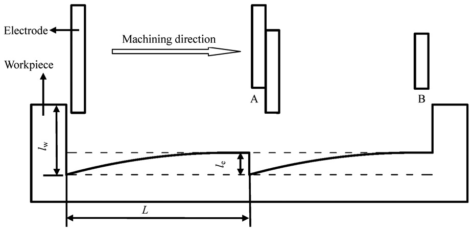
When fabricating complex 3D micro structures in EDM milling, the process could be considered as the repetition of monolayer machining. For machining each groove on one layer, an electrode first moves down into the workpiece to a previously set depth, and then it moves along a certain direction to conduct horizontal machining. When a cylindrical micro-electrode is used for EDM milling, the shape of the tool electrode changes rapidly during machining owing to serious electrode wear. Electrode wear occurs both at the end and on the side of the electrode, which are respectively characterized as end wear and corner wear. The end wear will lead to the reduction of the electrode length while the corner wear will cause the edge of the electrode to become round, thereby changing the electrode shape greatly. To avoid corner wear which can deteriorate the geometrical accuracy of a product directly, the uniform wear machining (UWM) method is widely used. After machining one layer, the electrode can maintain the original shape so that electrode wear is limited to occurring only at the end. The wear process of a micro-electrode in UWM is shown in Figure 1.
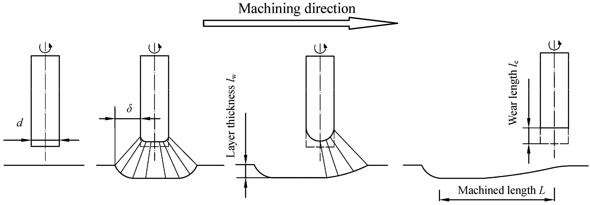
Diagram illustrating the principle of UWM.
However, the UWM method has some limitations: the productivity is low because the layer thickness is always around 10 µm and the geometrical accuracy of the products might be influenced by frequently scanning the same path because of the rotation of the flexible electrode. Therefore, increasing each layer thickness is a feasible way to solve these problems. The large layer thickness is usually between 10 and 100 µm, which will contribute to an arc and a tapering shape at the bottom part of the electrode during machining, as shown in Figure 2.
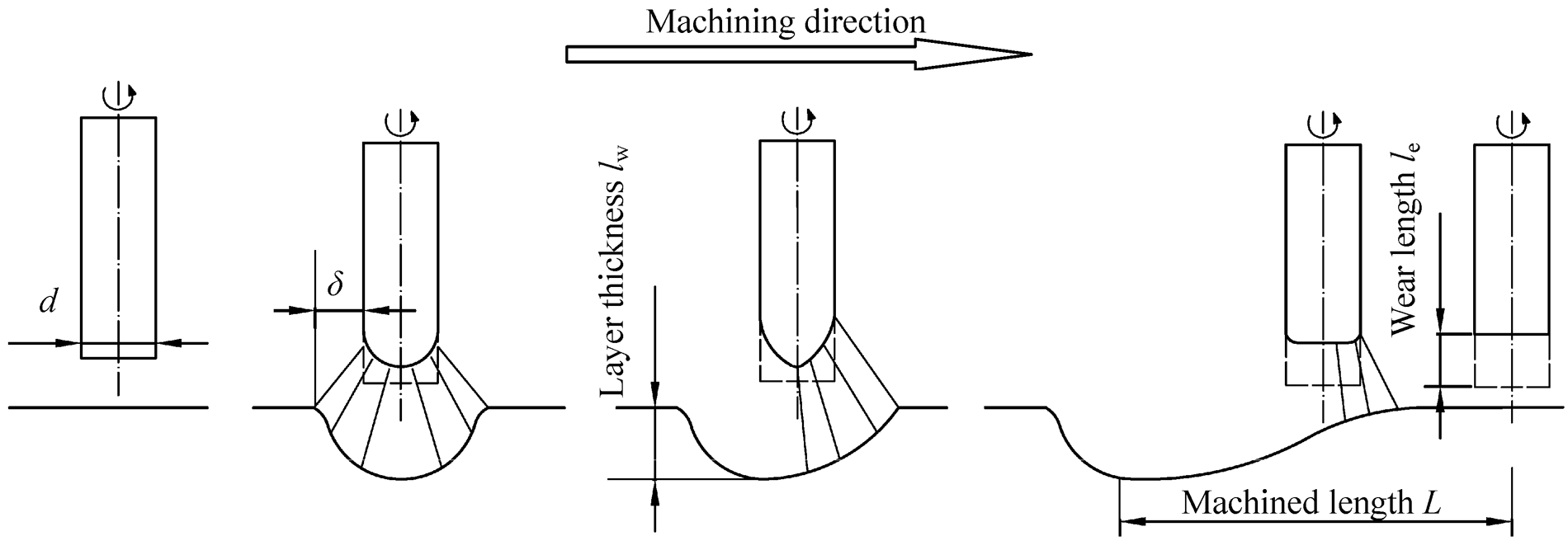
Diagram illustrating the principle of UWM based on large layer thickness.
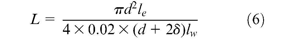
Figures 1 and 2 indicate that the bottom surface of the machined groove is inclined so that the electrode should be compensated in time during machining. To conduct electrode compensation, the wear model should be put forward first. In the UWM method, the electrode wear model is easy to establish. Because the electrode shapes before and after machining are almost the same, the electrode wear is only reflected in the reduction in length. Thus, the wear volume of the electrode can be calculated as

where Se is the section area of the electrode and le is the reduction in length (wear length). In the same way, the wear volume of the workpiece is given as

where Sw is the top surface area of the machined groove (in the horizontal plane) and lw is the machined depth (or the layer thickness). In ideal conditions, the section shape of the machined groove is rectangle so that Sw is calculated by

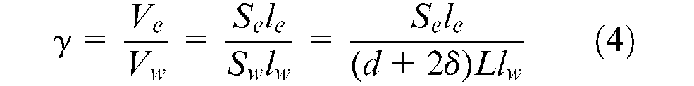
where d is the diameter of the electrode, δ is the machining gap, and L is the length of the machined groove. The volume wear ratio between materials of the electrode and the workpiece is denoted by γ. According to the scheme of the UWM method, an equation can be established as
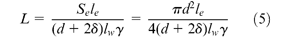
Electrode compensation will be conducted if compensation accuracy le is set beforehand. According to equation (4), the machined length where electrode compensation needs to be carried out can be obtained by
The above fix-length compensation model is obtained under the conditions that electrode wear occurs only at the end in the whole machining process and the machined depth lw of the workpiece remains unchanged during machining. However, the actual machining process is very complex so that it cannot be so ideal. As shown in Figure 1, the electrode edge is at first worn in the beginning and the electrode bottom becomes more and more blunt during the machining process, so that the cross-section shape of the groove cannot be a standard rectangle. In addition, although the electrode can recover its original shape, the machined bottom surface is apparently inclined because of the end wear of the electrode. Moreover, if compensation accuracy le is far smaller than the layer thickness, compensation will be conducted before the electrode can recover its original shape, and then the electrode wear is not uniform. All of this demonstrates that the wear volumes of electrode and workpiece cannot be simply calculated by the above formulas. Particularly in the case of large monolayer thickness machining all of the above problems could be more serious, so the electrode compensation model in equation (5) needs to be modified by processing tests.
Machining tests without electrode compensation
In this paper, tungsten electrode and red copper are used as a case to explain the modification of the electrode compensation model.
In order to conduct accurate electrode compensation under conditions of large monolayer thickness, first it is necessary to reveal the wear law of the micro-electrode during machining. Single-groove machining tests without electrode compensation are carried out using different processing parameters. Machining tests are conducted on our self-established high-precision micro-EDM system, which has a z-axis linear motor worktable with positioning accuracy of 2 µm, an x–y-axis alternating current servo motor worktable with positioning accuracy of 3 µm, a high-speed rotating spindle, a switch tube micro-energy resistor–capacitor (RC) pulse power supply, and an intelligent servo control system. The peak current is adjustable within 11 grades and the micro-energy RC pulse power has four external shunt capacitors of respectively 470 pF, 1000 pF, 2000 pF, and 4700 pF. The setup of the micro-EDM system is shown in Figure 3.
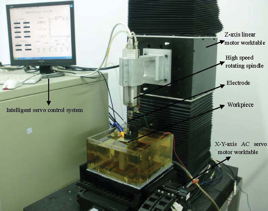
The high-precision micro-EDM system.
In non-compensation machining tests, electrodes first drill into the workpiece to certain depths and then move along the workpiece surface until discharge stops. Let the travel distance of an electrode be L, the electrode wear length be le, and the layer thickness be lw. The processing schematic is shown in Figure 4. According to the test results, it can be seen that the machined distances are different if using different processing parameters. In order to avoid frequent compensation, it is desirable that the electrode can be used effectively, which means that the machined distance L should be as long as possible in the same compensation accuracy le. In this case, the length of the electrode decreases most slowly and the bottom surface profile can be a gentle slope. Thus to gain the best processing results, effective processing parameters should be set first. Plenty of processing tests indicate that the main parameters which affect L most are capacitance C and layer thickness lw.
Processing schematic of micro-EDM milling without electrode compensation.
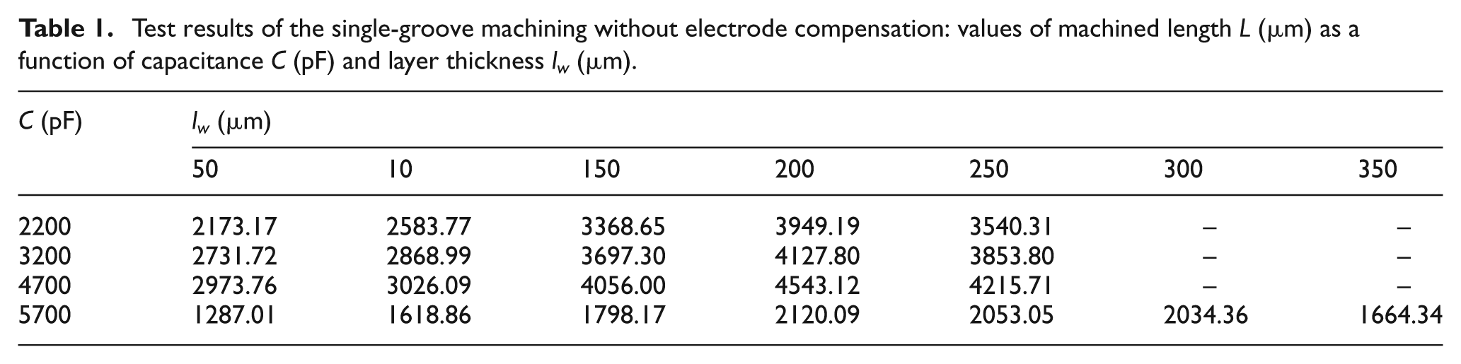
In the machining process, the capacitance can neither be set too small nor too large. A too-small capacitance cannot afford a large processing depth so that the machined length L is limited, while a too-large capacitance can accelerate the electrode wear and thereby shorten the machined length L as well. Moreover, when capacitance is set too large, the machined surface of the workpiece might be very rough. In the present tests, four commonly used capacitances are adopted which respectively are 2200 pF, 3200 pF (1000 pF + 2200 pF), 4700 pF, and 5700 pF (4700 pF + 1000 pF). The layer thickness is set as every 50 µm from 50 µm to 350 µm. The test results are shown in Table 1. When layer thickness is adopted as 300 µm and 350 µm the experiments are only conducted under the capacitance of 5700 pF, because the layer thickness is too large to be processed using small capacitances.
Test results of the single-groove machining without electrode compensation: values of machined length L (µm) as a function of capacitance C (pF) and layer thickness lw (µm).
The relationship between machined length L, capacitance C, and layer thickness lw is shown in Figure 5. It is obvious that the peaks of the four curves all appear at the same place where the layer thickness lw is 200 µm. The curve with the capacitance C of 4700 pF is above all of the other curves. So the best layer thickness lw and capacitance C are obtained to be 200 µm and 4700 pF. A photomicrograph of the groove machined using these two parameters is presented as Figure 6.
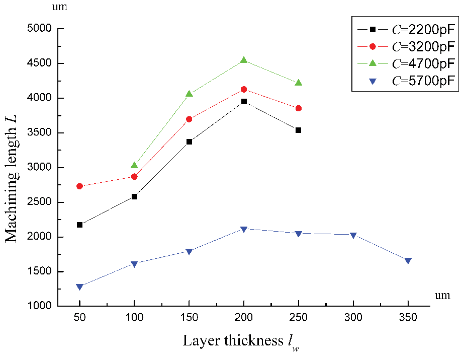
Relationship between machined length L, capacitance C, and layer thickness lw.
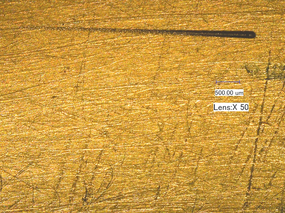
Photomicrograph of machined groove using lw = 200 µm and C = 4700 pF.
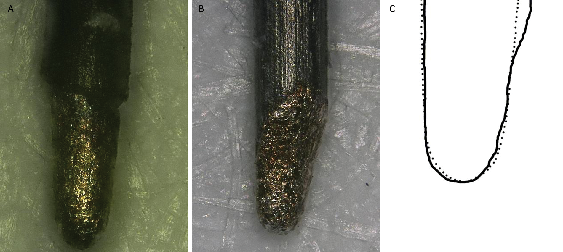
To analyze the relationship between electrode shape and machining length, electrodes which machined lengths of 300 µm, 600 µm, 1000 µm, 1400 µm, 2000 µm, 2400 µm, and 2800 µm respectively are collected; their photomicrographs are shown in Figure 7.
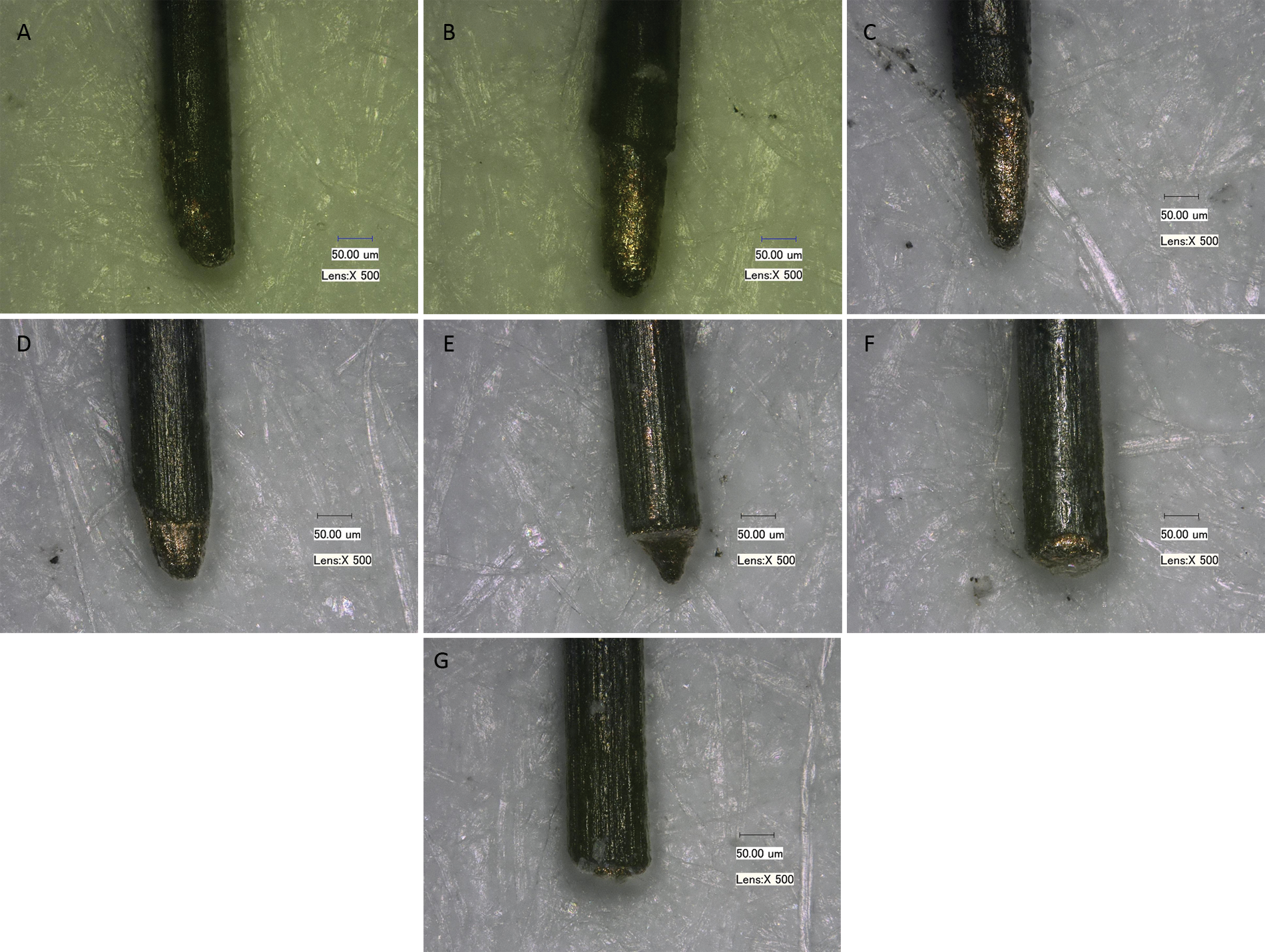
(a–g) Photomicrographs of electrodes after machining different lengths.
Figure 7 shows that in the beginning of the process, the corner wear of the electrode is more severe than the end wear, so the cylindrical electrode becomes a taper. But as the machining process proceeds, the end wear becomes severe and the taper turns into a hemisphere. At the end of the machining process, the electrode recovers its original shape. Therefore, if electrode compensation is conducted during the discharge process, the electrode will not recover its cylindrical shape. So the electrode shapes during the machining process should be studied in order to establish an accurate compensation model.
Modification of electrode compensation model based on large monolayer thickness
When processing with fix-length compensation, the shape of the end part of the electrode remains spherical or conical due to the point discharge phenomenon, which is clearly demonstrated by the experiments of the previous section. Therefore, the cross-section of the processed groove cannot be an exact rectangle so that the conventional model is not correct. Moreover, the shapes of the cross-sections are not consistent during the whole milling process because the electrode shapes are not the same after processing different lengths. It seems that there cannot be an exact general model which is suitable for any compensation accuracy but a compensation model for certain accuracy is possible to establish.
According to this problem, the antecedent compensation model is modified by experiments using a tungsten electrode to process copper and an improved compensation model based on large monolayer thickness is proposed as follows. To accurately establish the compensation model, a new relative volume wear ratio measurement method is first presented based on debris composition analysis. Next, a compensation length L is roughly calculated by equation (5) under a given compensation accuracy le. Then, fix-length compensation experiments are carried out using the obtained L and le, and the electrode shapes on the verge of each compensation are observed to modify the electrode volume loss amount between two continuous compensations. By comparing shapes of electrode and groove cross-section, the transect area is modified and the whole improved compensation model is established finally. Combined with the changing law of electrode shape in non-compensation milling process, the cross-section correction coefficient can be estimated under different compensation accuracies.
Measurement of relative volume wear ratio
To establish an accurate compensation model, an important value—the material relative volume wear ratio—should be given first. Conventional measurement methods are based on the calculation of geometry sizes of material worn volumes, which have great measurement errors. In this section, a new relative volume wear ratio measurement method is presented by analyzing the material composition of debris. This can effectively avoid the large errors caused by geometry measurement.
The major measurement steps of volume wear ratio based on debris composition analysis are as follows.
The major components of the two kinds of materials are first measured using an electron probe.
The chosen materials are used as electrode and workpiece respectively and the discharge machining process is conducted for some time.
After the processing test, the working fluid is carefully filtered in order to collect the electric erosion debris and the debris is then dried, to obtain the dried electric erosion powder.
The prepared electric erosion powder is placed into the stage of the electron probe and the content of each composition in the powder is measured quantitatively using the probe.
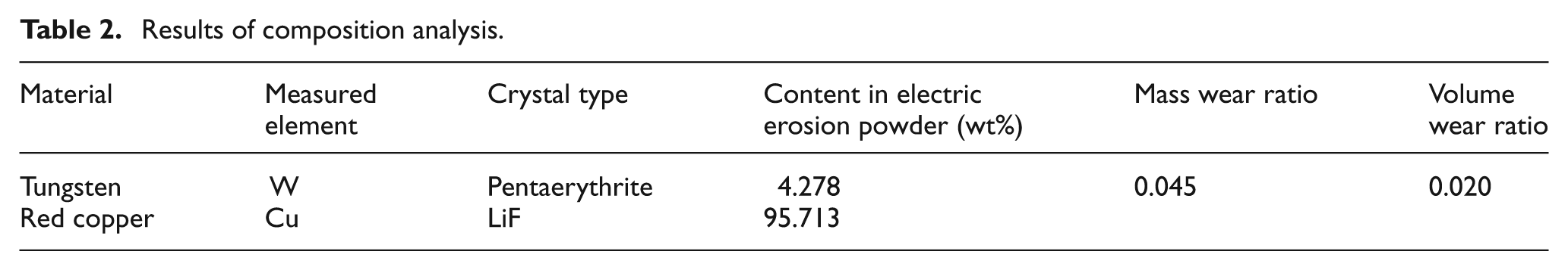
The quality wear ratio can be obtained by calculating the proportion of each component of electrode and workpiece materials and the volume wear ratio is finally obtained according to the material densities.
In the present tests, cold-drawn tungsten filaments with diameter of 0.1 mm are adopted as the electrode and the workpiece material is red copper. The density of tungsten and red copper is previously known as 19.35 g/cm3 and 8.46 g/cm3 respectively. Using electron probe microanalysis, the chemical composition of red copper is measured as: Cu + Ag = 99.9%, S = 0.005%, Pb = 0.005%, Fe = 0.005%, As = 0.002%, Sb = 0.002%, and Bi = 0.001% by weight. The processing parameters are voltage = 250 V, pulse width = 25 µs, pulse-off = 25 µs, peak current = 0.8 A, and capacitance = 1000 pF.
When using a tungsten electrode to process a red copper workpiece, the major element contents of the electric erosion powder are as shown in Figure 8 and the detailed analysis results of the electrical erosion powder are as shown in Table 2. The mass wear ratio is 0.045 and the volume wear ratio is 0.020.
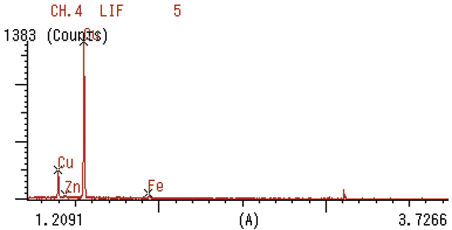
Composition of discharge debris produced by tungsten electrode and red copper workpiece.
Results of composition analysis
Therefore when using a tungsten electrode to process red copper, the value adopted for γ in the fix-length compensation model should be 0.02. In equation (5), the compensation length L should be expressed as
Worn volume modification
In this paper, the thickness of one layer is set as 200 µm and the compensation accuracy is given by 50 µm. The electrode diameter d and machining gap δ are known as 100 µm and 32 µm, so the compensation length L is calculated as 600 µm using equation (6). Experiments of fix-length compensation processing are carried out using these parameters. The machining process is shown in Figure 9.
Process diagram of fix-length compensation processing in micro-EDM milling.
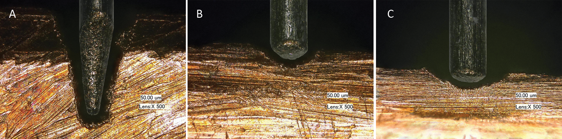
Electrode shapes are observed at the places where compensation is about to be conducted; for example, at points A and B in Figure 9. Photomicrographs of the electrodes at A and B are shown in Figure 10(a) and (b).
(a, b) Photomicrographs and (c) the superimposed picture of electrodes at locations A and B.
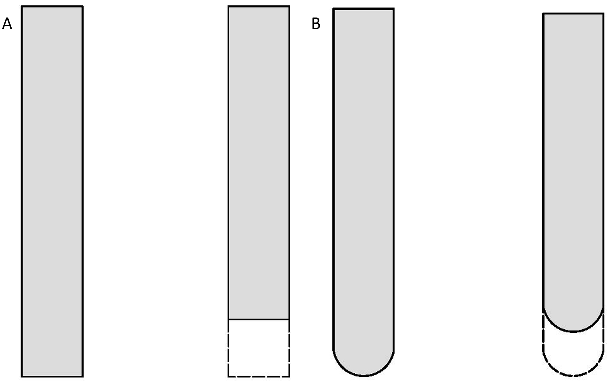
The profiles are extracted from the two photomicrographs of Figure 10(a) and (b) and superimposed as shown in Figure 10(c). It can be seen that the electrode shapes are very similar and are almost overlapping. This indicates that although the electrode constantly changes its shape during machining, it can still keep the same profile after it machines to the same length under certain compensation accuracy. Therefore, the electrode wear in this case can be also considered as uniform wear, as demonstrated in Figure 11. The wear volume in Figure 11(b) is equal to that in Figure 11(a) if their reduced lengths are the same. So, the wear volume of the electrode in equation (5) does not need modification.
(a, b) Electrodes before and after uniform wear machining.
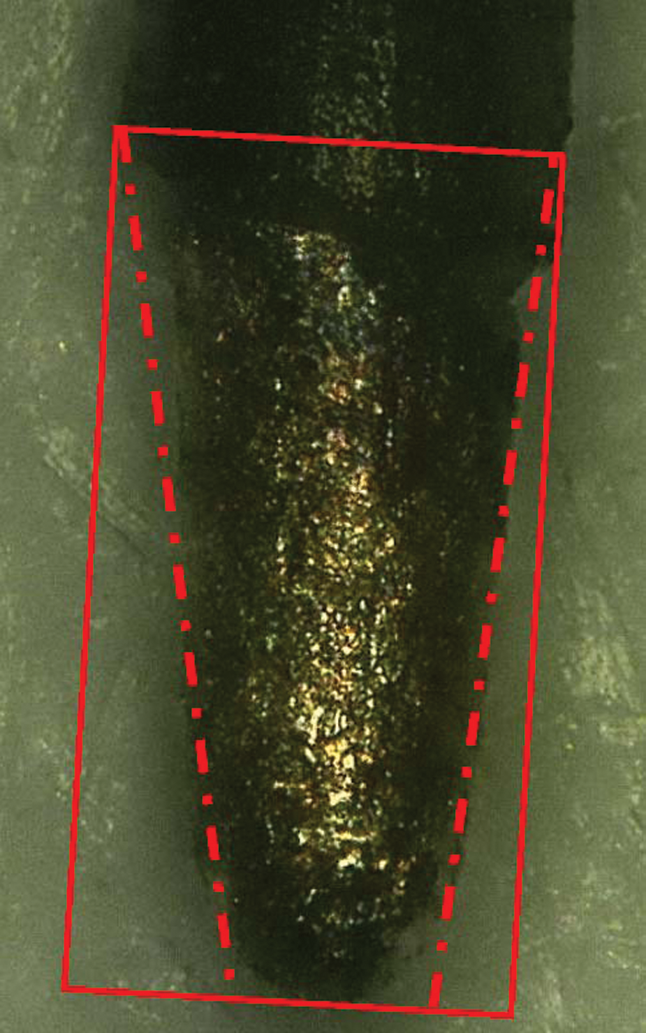
The cross-sections of the machined groove at different machining lengths during non-compensation machining are intercepted and the corresponding electrodes are observed as well. The pictures of cross-sections and the corresponding electrodes are combined to restore their processing relative places, see Figure 12. Compared with the electrode shapes, the cross-section profiles are almost parallel with the electrode profiles. Therefore, it is possible to amend the cross-section shape of the machined groove using the electrode shape.
(a–c) Combined pictures of groove cross-sections and their corresponding electrodes.
In this paper, an area coefficient Ks is introduced to correct the cross-section area of the workpiece. Because the compensation length L (600 µm) is not long, the electrode shape does not change much during two compensations, so that the change in electrode shape can be ignored. In present work, Ks is estimated to be 0.7 according to Figure 13, where the solid line presents the original profile of the electrode and the dotted line presents the electrode profile after machining. For any compensation accuracy in other processing tests, the Ks can be calculated by the electrode shapes obtained by non-compensation tests described in the section “Machining tests without electrode compensation”. From Figure 7, the relationship between the area coefficient Ks and the machining length L is as illustrated in Figure 14, which is not restricted by the electrode diameter and can be referenced for other compensation accuracies.
Approximate profile of the worn electrode after machining 600 µm.
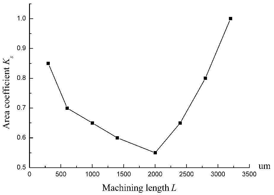
The relationship between area coefficient Ks and machining length L.
Moreover, the bottom surface profile is not a horizontal line because the machining depth changes with the reduction of the electrode length. Yu et al. have modeled the bottom surface profile of machined groove, which is approximately given by
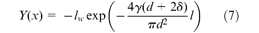
In the present work, lw is 200 µm, γ is 0.02, d is 100 µm, and δ is 32 µm. According to equation (7), the bottom surface profile in our work is obtained as shown in Figure 15(a).
(a, b) Bottom surface profile of the machined groove.
The compensation accuracy in the present test is 50 µm, so the bottom surface profile can be approximately considered a straight line, shown as the dotted line in Figure 15(b). Thus, the average depth of the machined groove is calculated to be 175 µm, so that a depth coefficient can be given as
After introducing in the volume coefficient Kv, the compensation model modification is finished and the improved electrode compensation method is established. In this paper, the compensation model is modified to be
Experimental work and discussion
Electrode compensation experiments were carried out respectively using the conventional compensation model of UWM, the modified compensation model proposed in this paper, and the layer-by-layer machining method of UWM. The experimental work was conducted on our self-established high-precision micro-EDM system as introduced in the section “Machining tests without electrode compensation”. The processing parameters are listed in Table 3.
Processing parameters.
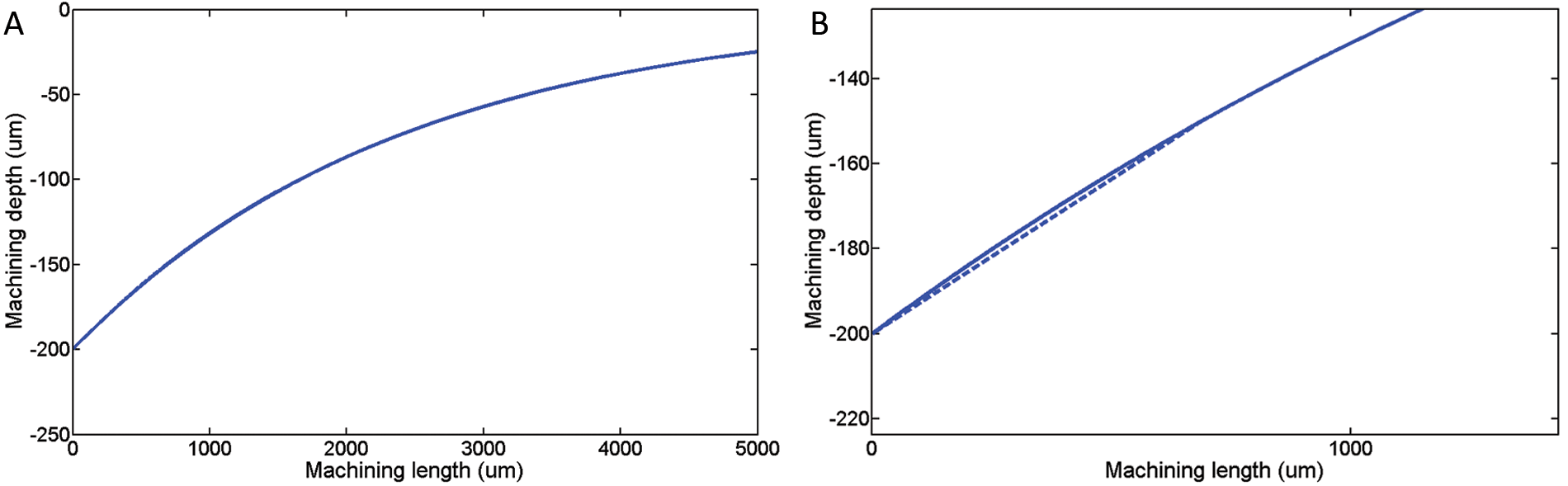
Case 1. A groove machining experiment was conducted using compensation parameters listed in Table 4, which were calculated by the conventional compensation model in equation (5). Figure 16(a) is the photomicrograph of the machined groove and Figure 16(b) is its cross-section photomicrograph. The machining direction is from right to left and the machining time is about 13 min. It can be seen that the groove in Figure 16(a) is not quite straight after conducting compensation twice (after machining for 1200 µm) compared with the part in the beginning. The cross-section after machining a length of 4000 µm is shown in Figure 16(b); its depth is measured as 328 µm, which is obviously much larger than the layer thickness of 200 µm. This means the groove is over-compensated during the machining process. So, case 1 shows that over-compensation will result in declines in machining precision and quality. That is because the micro-electrode is rotating and very flexible, so too large processing depth will lead to offset of the electrode discharging position.
Compensation parameters of case 1.
Photomicrographs of (a) the machined groove and (b) its cross-section for case 1.
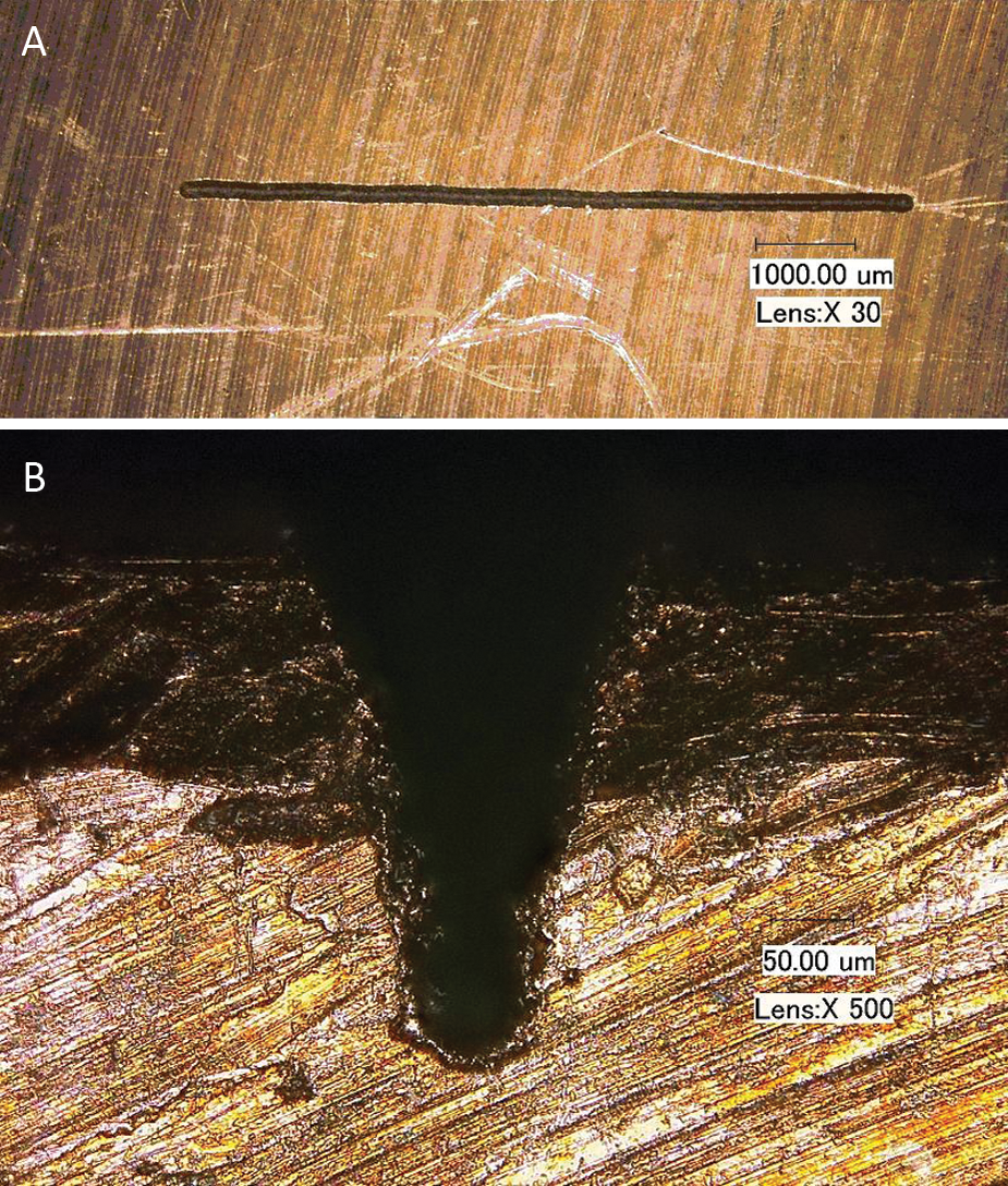
Case 2. A groove machining experiment was conducted using the compensation parameters listed in Table 5, which were calculated by the modified compensation model in equation (8). Figure 17(a) is the photomicrograph of the machined groove and Figure 17(b) is its cross-section photomicrograph after a machined length of 5000 µm. The machining direction is still from right to left and the machining time is about 15 min. It can be seen that the groove in Figure 17(a) is consistently straight in the full length and the depth of its cross-section in Figure 17(b) is very close to 200 µm, which is the desired monolayer thickness. Case 2 shows that the modified compensation model presented in this paper is correct and the precise compensation can ensure high machining precision and quality of micro-EDM milling.
Compensation parameters of case 2.

Photomicrographs of (a) the machined groove and (b) its cross-section for case 2.
Case 3. A groove machining experiment was conducted using the compensation parameters listed in Table 6. The layer thickness lw is adopted as 60 µm to simulate the UWM process. The compensation length L is calculated as 1200 µm by the UWM conventional compensation model in equation (6). The groove is machined layer-by-layer and the machining direction is first from left to right and then back to left. The total processing time is about 27 min. The machined groove photomicrograph is shown in Figure 18(a) and its cross-section photomicrograph is shown in Figure 18(b). It can be seen from the photomicrographs that the two machining paths are not quite coincident at the end of the machining, which causes the cross-section width to be inconsistent and much larger than that in case 2. Besides, the machined depth of the groove in case 3 apparently does not reach the set value. All of the above problems are also due to the flexible micro-electrode, which is made of cold-drawn filaments. When a flexible micro-electrode is rotating during micro-EDM milling, it can easily lower the machining reproducibility. Therefore, case 3 shows that when using the UWM method, machining layer-by-layer requires high-precision electrodes. But a high-precision electrode is very expensive and time consuming to prepare, which is not appropriate if machining in large quantities.22,23 Moreover, the machining time in case 3 is almost twice that in case 2. The machining efficiency of UWM is pretty low compared to large monolayer thickness machining.
Compensation parameters of case 3.
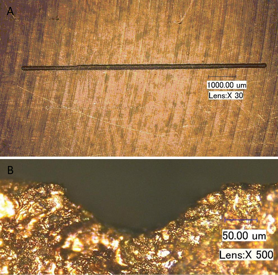
Photomicrographs of (a) the machined groove and (b) its cross-section for case 3.
The above experiments indicate that the improved electrode compensation method proposed in this paper can significantly enhance the processing quality and efficiency of micro-EDM milling, and the introduction of large monolayer thickness can effectively reduce the geometrical errors caused by poor reproducibility, thus guaranteeing the machining precision of micro-EDM milling.
The photomicrographs of Figure 19 show machined examples using the modified compensation parameters given in Table 7. Figure 19(a) is part of a map of China and Figure 19(b) is a piece of clover. The photomicrographs show that the machined lines are uniform and consistent, so the proposed electrode compensation modification method is an effective way to improve the electrode wear model and to find the accurate compensation length in micro-EDM milling.
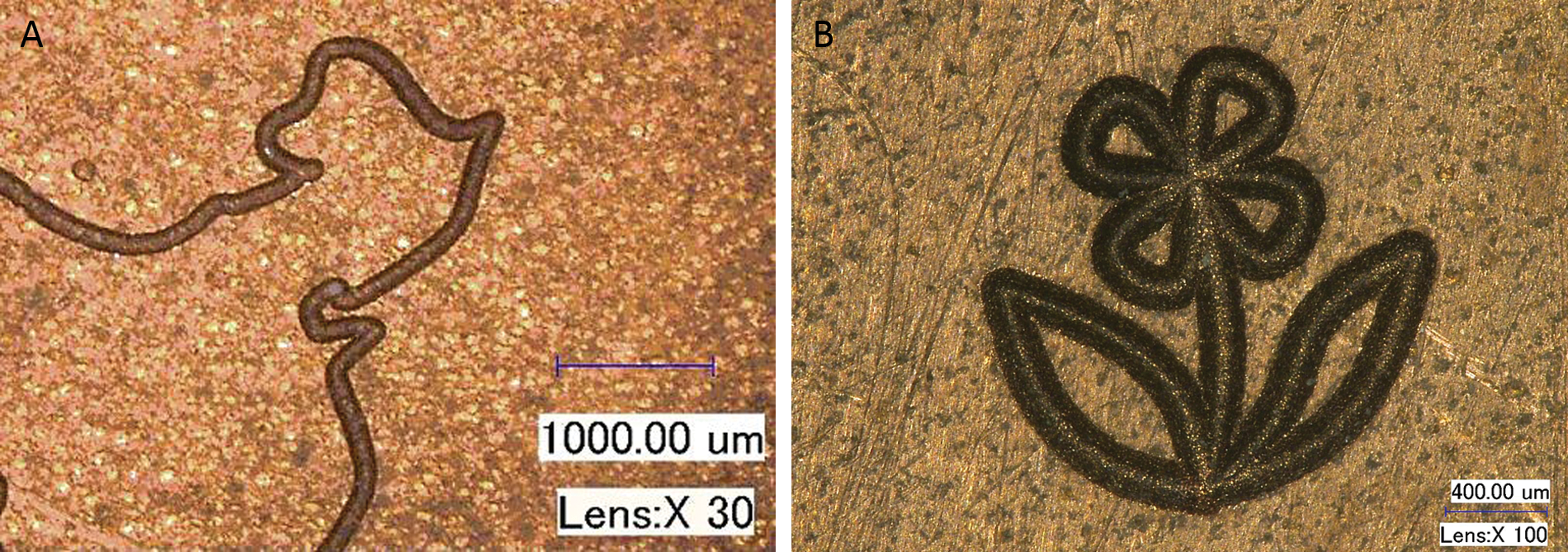
(a, b) Photomicrographs of grooves machined using the improved electrode compensation method.
Experimental setups.
The improved electrode compensation method can also make a contribution to machining of 3D micro structures. In our present work, micro pyramids are fabricated using layer-by-layer machining methods of the conventional and improved UWM models. The pyramids have three layers and the tool path of each layer in the X–Y plane is shown in Figure 20. The black circles represent the starting points. The electrode follows the paths until it arrives at the white circles, which represent the end points. Photomicrographs of the machined micro pyramids using conventional and improved compensation models are respectively shown in Figure 21(a) and (c). Figure 21(b) and (d) are their corresponding height curves of longitudinal sections where marked in red lines on the photomicrographs. It is obvious that the improved electrode compensation model can achieve much better processing quality compared to the conventional UWM model. Therefore, the proposed electrode compensation modification method based on large monolayer thickness can also provide significant references in development of the 3D theory of micro-EDM milling.
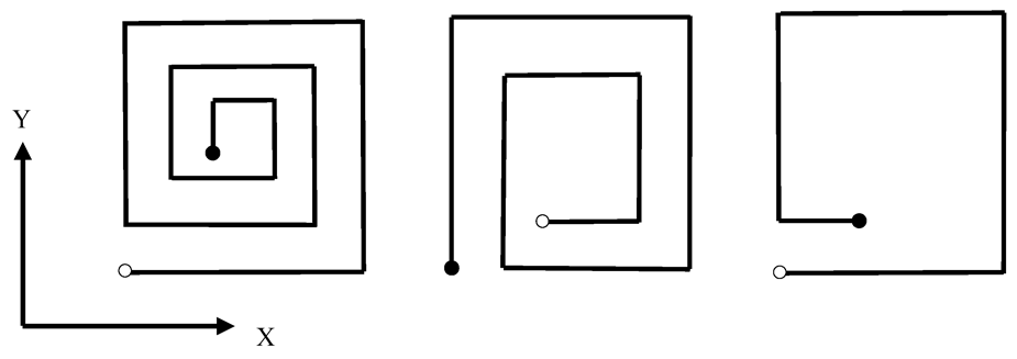
Tool paths in the X–Y plane.
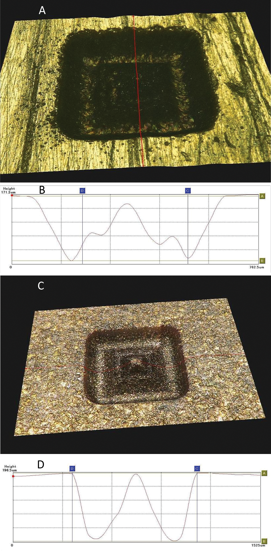
(a, c) Photomicrographs of the machined micro pyramids and (b, d) their height curves using conventional (a, b) and improved (c, d) electrode compensation methods.
Conclusions
For the purpose of enhancing the machining quality and efficiency of micro-EDM milling, a large layer thickness milling method is introduced and the improved electrode compensation model for large monolayer thickness milling is proposed based on modification of the conventional compensation model. First, non-compensation processing tests are conducted to properly select the processing parameters. Second, the wear law of the micro-electrode is investigated and the fix-length electrode compensation model is modified by taking into consideration the changes of electrode shape during machining. A new relative volume wear ratio measurement method is also presented based on material composition analysis, which can avoid the geometrical measurement errors that occur in conventional measurement methods. Electrode compensation experiments are carried out respectively using the conventional compensation model of UWM (case 1), the modified model proposed in this paper (case 2), and the layer-by-layer machining method of UWM (case 3). Experimental results show that using the conventional compensation model will lead to over-compensation and the layer-by-layer machining method is time consuming and of poor reproducibility. However, the modified compensation model proposed in this paper can ensure high machining efficiency and high machining precision and quality of micro-EDM milling. The proposed modification method will provide meaningful references to develop 3D machining theory and methods of micro-EDM milling.
The materials of the electrode and the workpiece used in this paper are tungsten and red copper respectively. Since the processing tests and relative volume wear ratio measurement are based on these two kinds of materials, the parameters in the present work cannot be directly used if choosing different processing materials. However, the model modification process is easy to repeat. Plenty of experiments on other materials will be carried out using other materials in our future work, to establish a database of electrode compensation values for all kinds of processing materials.
Footnotes
Appendix
This work was supported by the Research Fund for the Doctoral Program of Higher Education of China [grant number 20090041110031] and the National Natural Science Foundation of China [grant number 51005036].