
Abstract
Additive manufacturing (AM) has significantly transformed the fabrication of functional materials, particularly in electronics and biomedical engineering. This study reviews stereolithography (SLA), selective laser sintering (SLS), fused deposition modeling (FDM), direct ink writing (DIW), and inkjet printing for flexible electronic applications. The review highlights SLA-based 3D printing’s better ability to optimize material compositions, printing procedures, and post-processing methods to improve material characteristics. Photosensitive materials and shrinkage-induced internal tensions seems to be its major constraint. Additionally, SLS 3D printing has improved composite materials' electrical, mechanical, and thermal properties. It has drawbacks including permeable structures and internal tensions. In FDM 3D printing, mechanical and electrical qualities are improved for piezoelectric sensor manufacture. Warping and nozzle blockage require additional study. DIW’s versatility in constructing complicated structures with increased features for energy harvesting and sensor development is also mentioned. We identify ink development and printer nozzle clogging issues. The review concludes that inkjet printing can provide a variety of materials for flexible electronics. Since it integrates the latest discoveries with technological developments, this study may help guide future research and promote innovation in the sector. Overall, additive manufacturing methods provide a new era of sensor technology by offering unrivalled flexibility and versatility.
Keywords
Introduction
Sensor manufacturing is a popular topic of research in the material research community particularly for flexible electronics as well as bio-compatible sensors. Researchers are currently focusing on two primary aspects of sensors: (a) cost and (b) sensing capability. Presently the sensors for electronics applications are being manufactured using methods such as: Fused Deposition Modelling (FDM), 1 Direct Ink Writing (DIW), 2 Aerosol Jet Printing (AJP), 3 Stereolithography (SLA), 4 Direct Light Processing (DLP), 5 Two-photon Lithography, 6 Binder Jetting 7 and other such technologies. The flexible sensors are classified into various categories based on their applications, 8 such as force, humidity, pressure, temperature, gas sensor, light and pH etc. The flexible sensors can be classified into two groups according to how they can be used: stationary sensors that stay in one location and mobile sensors that can generate and interpret data while moving around. The goal of numerous investigations has been to create flexible electronic sensors that can monitor various aspects of the workplace.9–11 The issue with dealing with flexible sensing materials is their efficiency, cost, and preparation complexity. 12 Though, the sensors produced using the 3D additive manufacturing techniques have constraints in terms of size, shape, and flexibility and in order to be more generic and resilient, the sensors must be designed to be flexible enough to be mounted to any surface without losing their characteristics. The flexibility of the sensor is determined by its materials, thickness and the shape.9–12
A significant focus in the flexible electronics domain has been to develop noble materials to achieve better performance and life of the sensors. The first studies on piezoelectric materials began in the 1880s, when French scientists Jacques Curie and Pierre Curie discovered that quartz crystals had a positive piezoelectric effect.13,14 One year later, G. Lippmann discovered the reverse piezoelectric effect. 15 Since then, researchers have investigated several combinations of piezoelectric materials including: ceramics, nano-composites, piezoelectric polymers, and polymeric composites. 16 Such materials are aimed to offer good piezoelectric characteristics along with greater mechanical flexibility, durability, ductility, stability, and adaptability to a variety of structural forms. Out of the aforesaid materials, the piezoelectric crystals may not be ideal for applications requiring mechanical flexibility, such as bends and rotations. Flexible electronic materials have been classified into three categories: (a) ferroelectric polymers, (b) biopolymers, and (c) polymeric composite-based piezoelectric materials. 17
The sensor manufacturing technologies have been tested with several new materials compositions depending on their capabilities, such as material flowability, compatibility with the chosen process, and so on. For example, FDM-based 3D printing process often works with sub-solid-state thermoplastics whereas extrusion such as Polylactic Acid (PLA), Nylon (PA6), Acrylonitrile Butadiene Styrene (ABS), and so on.
18
Similarly, the DIW approach works with elastomers, metal ceramic micro particle solutions, and biomaterials.
19
The DLP-based technology uses polymers that can be cured using UV or LED light.
20
Experts are focusing on development of sensors for data acquisition for various day-to-day activities in order to make human life more comfortable. One such application in this field is active and assisted living (AAL) which helps in recognising the human activities in open environment and assist the user in predefined tasks.
21
The preceding two decades have seen a significant growth in chronic diseases, necessitating the development of more suitable technologies capable of monitoring human actions in daily life and communicating with the user so that precautionary measures can be taken before occurrence of substantial injury to the human body.
22
Overall, the 3D printing technologies offer a promising paradigm for fabrication of thin film flexible sensors using various combinations of nano-additives for enhancing the electronic and mechanical performances. In this paper we have compiled the literature pertaining to the evolution of the 3D printing/additive manufacturing technologies for fabrication of thin film sensors.
Scope of the review paper
Over time, piezoelectric materials have become extensively accepted and explored for the creation and improvement of the material spectrum of flexible piezoelectric devices. As additive manufacturing continues to catalyse material synthesis advancements, particularly in electronics and biomedical engineering, a profound comprehension of the capabilities and constraints of these techniques becomes imperative for researchers, engineers, and industry practitioners alike. Figure 1 depicts the outline of additive manufacturing and details the different aspects of 3D printing, which are most important for the current work. Furthermore, the paper intends to thoroughly investigate the characteristics and techniques for creating electroactive composites. The article also highlights the issues and opportunities associated with such 3D printing technologies. Further a special focus is given on the material synthesis of conductive ink using inkjet 3D printing technique. Overview of additive manufacturing with different aspects of input available in 3D printing.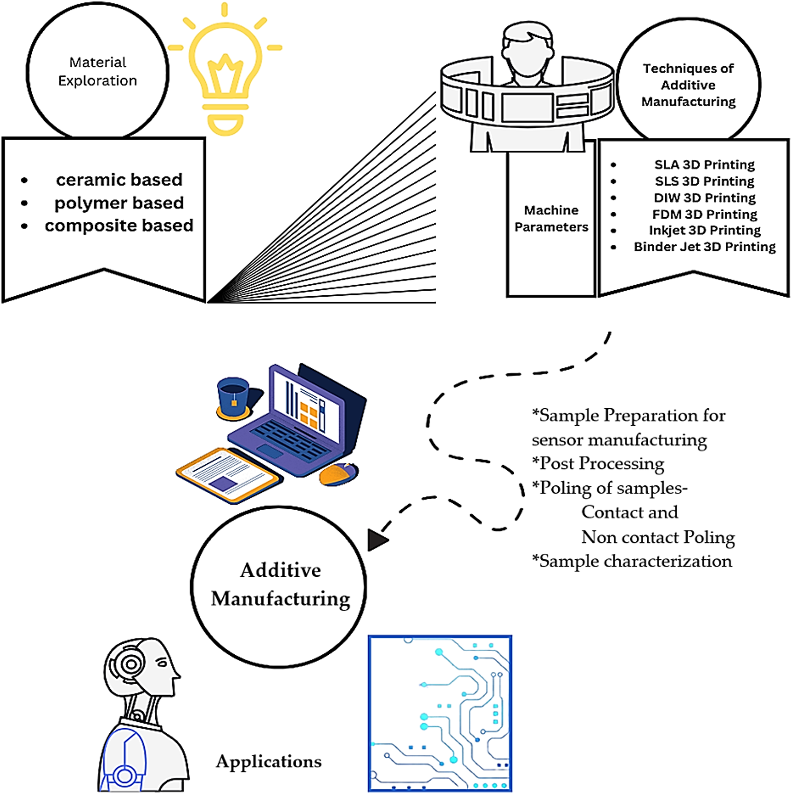
Overview of different 3D printing techniques capable of printing electroactive polymer
Electroactive polymers (EAPs) have the potential to power a new generation of soft robotics and actuators because of their lightweight, flexibility, and electrical stimulation responsiveness. 3D printing offers a variety of manufacturing options for complex EAP structures. Researchers may use 3D printing technology to build elaborate patterns that are tough to produce using standard manufacturing processes. This enables more customisation and innovation in the realm of soft robotics. As technology advances, we should expect even more revolutionary uses of EAPs in a variety of sectors. Researchers are investigating the potential of electroactive polymers (EAPs) to revolutionize soft robotics and actuators due to its lightweight nature, flexibility, and ability to respond to electrical stimulation. Various 3D printing processes are available these days which are capable of manufacturing electroactive polymers, such as stereolithography (SLA), 23 fused deposition modeling (FDM), 24 and selective laser sintering (SLS), 25 inkjet printing (IP), 26 Direct ink writing (DIW) 27 etc. When printing electroactive polymers, each of these processes has its own set of benefits and obstacles. Stereolithography, for example, offers great resolution and a clean surface finish, making it perfect for complex designs. Fused deposition modeling, on the other hand, provides quicker printing rates at a lesser cost. Selective laser sintering is well-known for its ability to precisely print a wide range of materials, including electroactive polymers. Overall, the choice of 3D printing technology will be determined by the project’s unique needs and the desired attributes of the finished product.
SLA based electroactive polymer printing
SLA-based 3D printing involves the use of a build platform where very viscous material is spread out. Then, certain curves and regions are solidified using a UV laser. The SLA printer utilizes a laser beam curing system and galvanometric mirrors to direct the laser beam onto a photosensitive substance, which is then utilized for 3D printing. The SLA 3D printer has the capability to print layers with a thickness that may vary between 10 and 50 µm, and it can achieve an XY resolution of 30 µm. Thus far, the SLA platform has been utilized to process a diverse range of materials. SLA 3D printing has established a foundation in the production of optical equipment. Various materials have been tried since the year it was first introduced, 1984. The researchers have investigated various combinations of photosensitive materials and systems to obtain improved outcomes for new products.
Sotov et al. 28 employed an LCD-based SLA system to investigate lead-free barium titanate (BaTiO3, BT) piezoceramics. The study found a dielectric constant of 1965, Tanδ%: 1.7, and d33 coefficient: 200pC/N for a 3D printed SLA sample of ceramic BaTiO3 material.
Smirnov et al. 29 investigated several sizes of the BT material matrix for slurry preparation and compared the conventional method to the SLA technique for specimen production. The study found that SLA outperformed conventional methods in terms of piezoelectric and Tanδ properties, while being cost-effective. The problem of irregular grain development in conventional techniques was likewise eliminated in the SLA approach. Chen et al. 30 used a mask-image-projection (MIP)-based SLA approach to study BT nanoparticles (100 nm). The investigation yielded a piezoelectric constant of 160 pC/N and a relative permittivity of 1350. The work created a specimen with piezoelectric properties that may be used in an ultrasonic transducer for energy focussing and sensing. Wang et al. 31 established a novel process for preparing piezoelectric ceramic paste by grafting oleic acid onto the surface of PZT. The paste with 72 wt% PZT material exhibited 30 mVk/Pa electrical sensitivity.
Cheng et al. 32 conducted a similar investigation, fabricating an ultrasonic array using the SLA method, to explore the potential of BT-based piezoelectric materials in ultrasonic transducer applications. The developed material composition of 80 wt% of BTO, displayed 166pC/N of piezoelectric coefficient. Kim et al. 33 employed a PVDF-based matrix to investigate piezoelectric properties using SLA. The study found that a 2 wt% ratio of PVDF in photopolymer resin (PR) and a mixing ratio of 1:10 resulted in ±0.121 nA under 80N loading conditions. Wang et al. 34 studied for BT nanoparticle loading ratio for optimum piezoelectric characteristics and discovered that 40% of BT nanoparticles had a low viscosity of 232 mPas and a shear rate of 46.5/s. After post-treatment, the ceramic composite had a piezoelectric coefficient of 163pC/N.
Xing et al. 35 looked at developing a high solid loading Al2O3 suspension for SLA-3D printing micro-components with intricate shapes. The suspensions, which comprise coupling agents containing silane and low viscosity acrylic monomers, have superior wettability and rheology behavior, with a density of 99.5% achieved by the SLA process and sintering. When integrated with a 75 wt% Al2O3 suspension, the KH560-based Al2O3 matrix demonstrated elevated wettability. The study by Sun et al. 36 employed numerous dispersants to examine the consistency and other characteristics of a suitable slurry suspension of nano zirconia particles for piezoelectric capabilities by employing SLA platform. The investigation demonstrated that 3 wt% BYK was the optimal dispersion for preparing a suspension of nano zirconia particles. This suspension was used to produce a zirconia component, which shrank significantly in the X-Y and Z directions by 21.9% and 28.9%, respectively.
The investigation performed by Xing et al. 37 revolves around synthesising the UV-curable pastes containing Zirconia Toughened Alumina (ZTA) composites, wherein the manipulation of Al2O3 particle sizes and ZrO2 quantities is conducted via a modified Krieger-Dougherty formulation. A concoction comprising 30 vol% fine Al2O3 particles and 70 vol% large Al2O3 particles manifests the most diminished viscosity. Conversely, formulations harboring 20 vol% ZrO2 showcase an escalation in viscosity concurrent with a decrement in curing depths, ascribed to diminished inter-particle spacing and exacerbated light diffusion effects. The resultant ZTA ceramics evince heightened flexural strength, fracture toughness, hardness, and relative density. Ulkir et al. 38 utilized the microelectromechanical system (MEMS) framework to scrutinize a piezoelectric material-incorporated cantilever design for an integrated circuit. The investigation subjected the piezoelectric cantilever to tip displacement assessment via an external electric field. The analysis unveiled that a cantilever characterized by dimensions of 900 µm in length, 225 µm in breadth, and 40 µm in thickness showcased a maximal tip displacement of 14.98 µm upon application of a 10V voltage. These findings exhibited congruence with the outcomes derived from simulations executed employing the finite element method (FEM) and the COMSOL Multiphysics software.
Zheng et al. 39 delved into the investigation of Pb(Mg1/3Nb2/3)O3-PbTiO3 (PMN-PT)-based relaxor ferroelectric systems, demonstrating their potential for advanced electromechanical device applications. Their study implemented a novel approach involving a ternary composite matrix of 1%-Sm-PMN-29PT, employing the concept of textured engineering using SLA technique. This technique enhanced alignment and orientation control within the ceramics, resulting in remarkable d33 values of 652 pC/N and 800 pm/V, respectively. Roca et al. 40 delved into the multi-layered fabrication of a bioinspired tympanic membrane (TM) modeled after the structure found in locust ears, employing a biomimetic approach. The printing process entailed the modulation of thickness to effectively correspond to distinct acoustic frequencies. The investigation successfully showcased the production of TM membranes utilizing diverse layer materials with varied thicknesses, elucidating the correlation between acoustic signals and voltage responses emanating from sources of differing frequencies.
The findings underscore the versatility and potential of SLA-based 3D printing in exploring and enhancing various materials' properties for specific applications. From investigating lead-free piezoceramics to synthesizing UV-curable pastes containing composites, each study delves into optimizing material compositions, printing techniques, and post-processing methods. Through meticulous experimentation, researchers have achieved remarkable advancements in piezoelectric, mechanical, and electrical properties, paving the way for innovative applications in fields such as ultrasonic transducers, electromechanical systems, and bioinspired structures. These findings collectively contribute to the growing body of knowledge in materials science and additive manufacturing, offering insights into the manipulation of material properties at the microstructural level for tailored functionalities and improved performance in various engineering applications. Further the SLA based 3D printing has some challenges or constraints due to the technique of printing. It requires photosensitive material that can be photon cured in presence of laser beam. Further, the material experiences shrinkage while getting solidified resulting in internal stresses in final product.
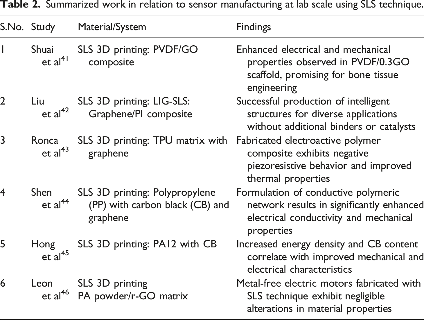
Summarized work in relation to sensor manufacturing at lab scale using SLA technique.
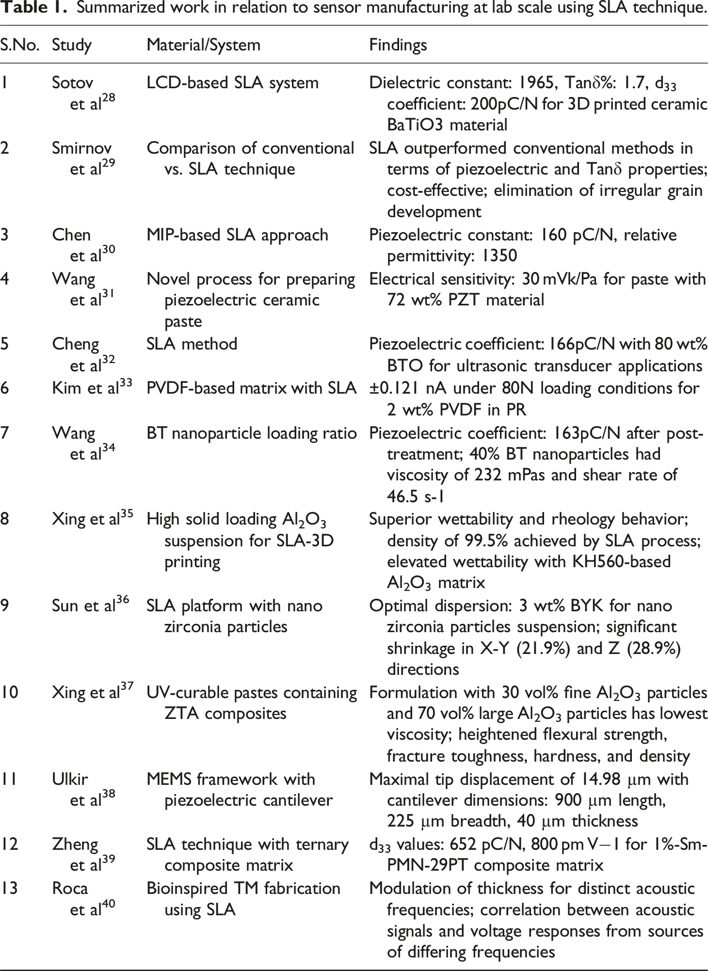
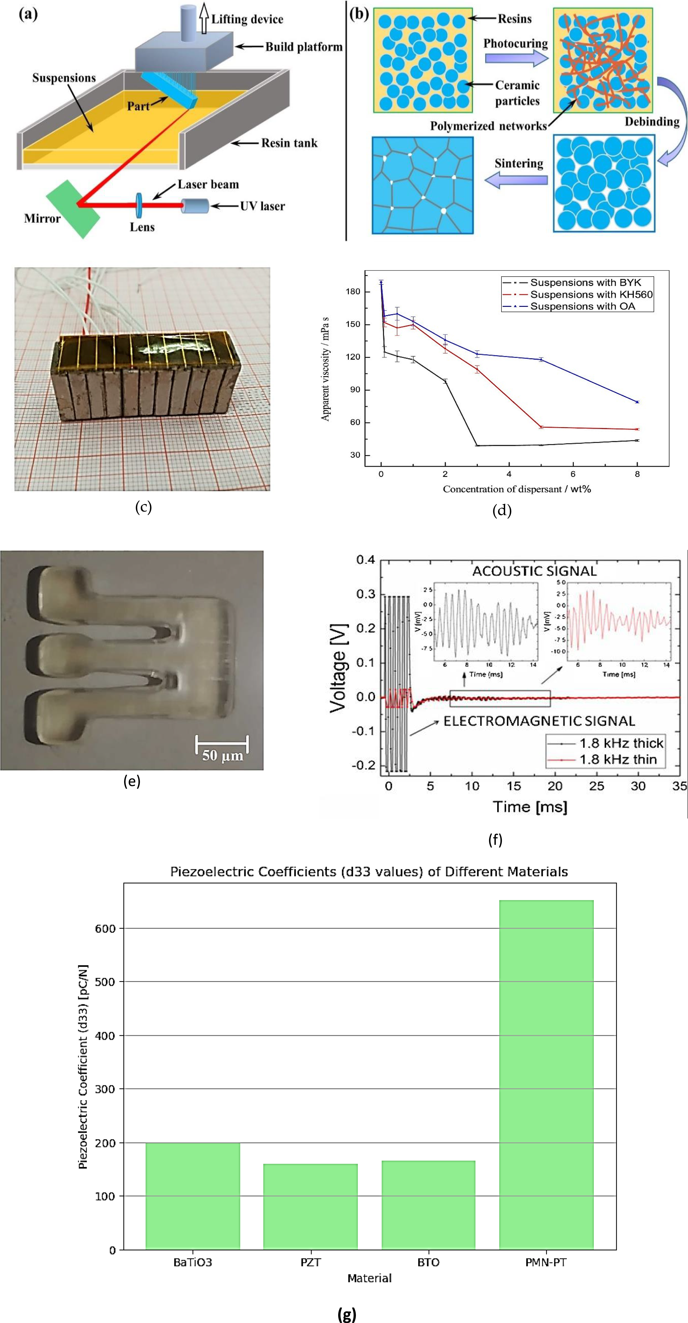
(a) Different stages of SLA printing and (b) post processing (Reused with the permission of Ref. 34); (c) SLA printed ultrasonic array (Reused with the permission of Ref. 32); (d) Apparent viscosity in relation to concentration of different suspensions (Reused with the permission of Ref. 36); (e) Piezoelectric material 3D printed using SLA technique (Reused with the permission of Ref. 38); (f) Acoustic and voltage signal with its two well-differentiated regions at 1.8 kHz (Reused with the permission of Ref. 40); (g) Piezoelectric coefficient value for different materials for SLA 3D printing.
SLS based electroactive polymer printing
SLS is a technique where laser is used to melt the material at selective position with preset profile using suitable CAD model. The material is in powder form and is spread over the build platform. No further support is required by the powdered material. The technique is generally used with metallic powder and components but it has also been explored for polymeric material matrix by some of the research groups.
Shuai et al. 41 harnessed the potential of selective laser sintering (SLS) 3D printing to fabricate a composite matrix of Polyvinylidene fluoride (PVDF) enriched with graphene oxide (GO). The chemical functionalities of GO engendered robust hydrogen bonding interactions with PVDF’s fluorine moieties, prompting a transition from the α to the β phase. Remarkably, the PVDF/0.3GO scaffold demonstrated amplified electrical output metrics, enhanced cellular responses, and bolstered mechanical integrity in both compressive and tensile regimes. These revelations illuminate the exciting prospects for leveraging such constructs in the intricate landscape of bone tissue engineering. Liu et al. 42 have put forth a pioneering methodology employing laser-induced graphene (LIG)-SLS for crafting bulk graphene and Polyimide (PI) composite freeform structures. This innovative technique eliminates the need for additional binders, catalysts, and templates, relying solely on PI powder for the fabrication of graphene-based structures. The investigation utilized CAD-guided laser irradiation scribing to meticulously process each layer, implementing a selective slicing pattern to craft intricate Graphene/PI hybrid structures. This cutting-edge approach has enabled the successful production of LIG-AM-enabled intelligent devices and structures tailored for diverse application scenarios.
Ronca et al.
43
harnessed a TPU matrix integrated with graphene amalgamation to fabricate an electroactive polymer composite tailored for electronics applications. The investigation encompassed a spectrum of inbuilt structures and porosity ratios ranging from 20% to 80%. The findings elucidated the composite’s propensity for negative piezoresistive behavior. Notably, within the array of inbuilt structures on the SLS platform, the Schwarz structure exhibited superior characteristics concerning gauge factor (GF) and elasticity. Furthermore, the incorporation of graphene yielded enhancements in the thermal stability and glass transition temperature of the TPU matrix. Shen et al.
44
delved into the integration of carbon black and graphene nano sheets (GNS) within a polypropylene polymer matrix to engineer a conductive network with a three-dimensional structure employing the selective laser sintering (SLS) platform. The investigation entailed the meticulous optimization of filler loading at 2 wt% and a CB:GNS ratio of 7:3 to formulate a polypropylene composite with a conductive polymeric network. The resulting composite showcased a remarkable enhancement, achieving an eight-order magnitude increase in electrical conductivity compared to the pure polypropylene matrix, coupled with notable improvements in its mechanical properties. Figure 3 shows the (a) Schema of SLS technique and printed part of PVDF/Graphene (Reused with the permission of Ref. 41); (b) multi parts printing using LIG-SLS technique and (c) PI/Graphene composite using multi parts printing ((b) and(c): Reused with the permission of Ref. 42).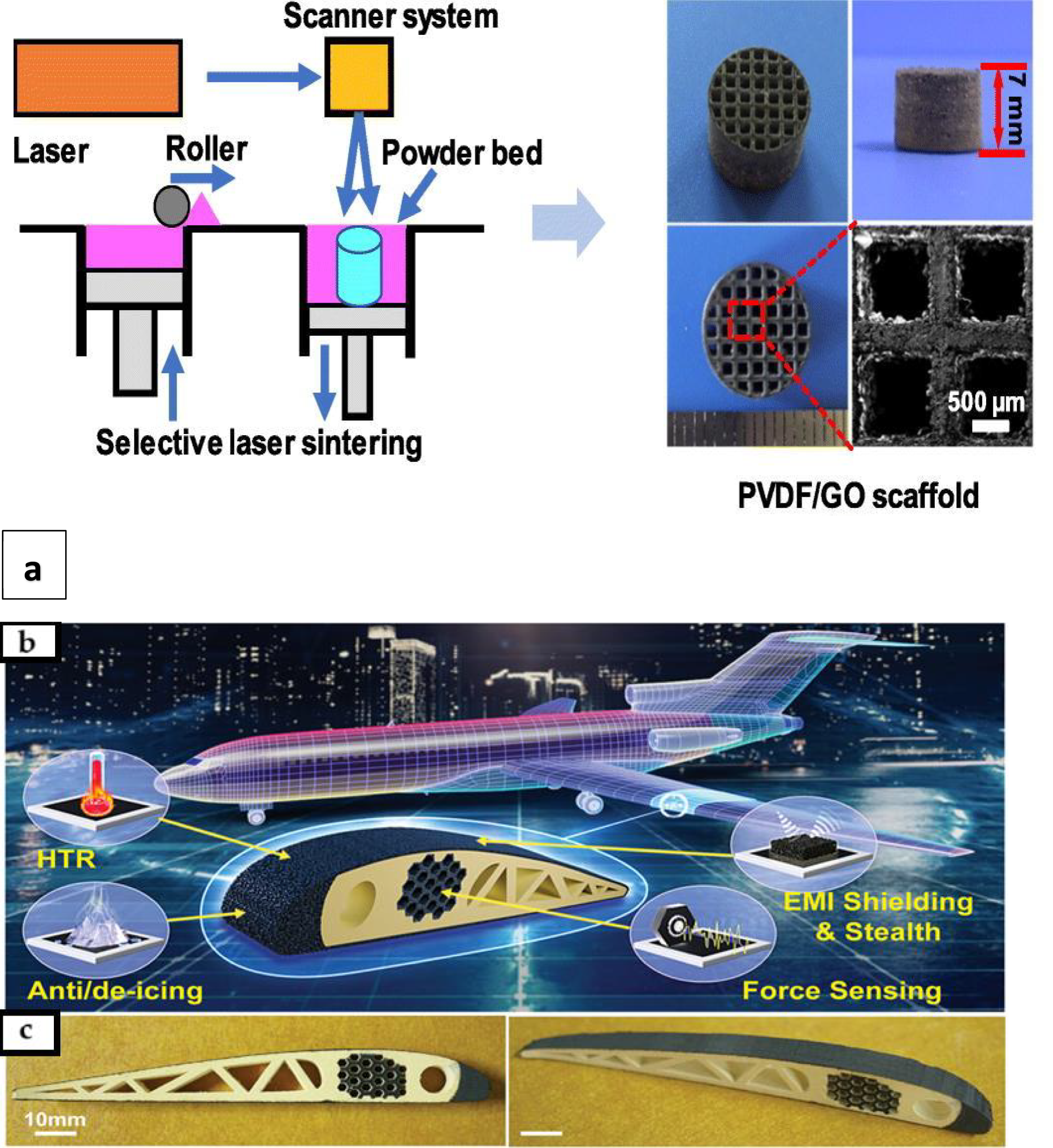
Summarized work in relation to sensor manufacturing at lab scale using SLS technique.
FDM based electroactive polymer printing
The widespread use of 3D printing to create intelligent electrical devices has accelerated the development of several composite material matrices capable of inducing piezoelectric phenomena. Concurrently, intrinsic problems beset the 3D printing process, particularly when dealing with SLS and SLA procedures, which include issues such as the necessary support structures, material restrictions, and associated expenses. Nonetheless, these limitations are overcome by using the Fused Deposition Modeling (FDM) technology, which involves 3D printing with an extrusion head guiding filament made of the necessary materials. A wide range of scientific attempts have been made to address the development of filaments intended for FDM printing of piezoelectric materials. The technique is based on tractor trolley mechanism where a feedstock material is fed through nozzle at necessary temperature on build platform and deposited in layer-by-layer fashion. The flexibility of technique in relation to the material choice which may be developed at lab scale is one of the greatest advantages of the FDM technique.
Duque and Murillo 47 examined FDM printing using commercially available PVDF material and two parallel electrodes for connections. To build a monolithic harvester, the study employed FDM printing. The analysis attained a maximum output voltage of 1.46 mW by applying a 4MΩ impedance load. Simunec et al. 48 researched the use of FDM printing for thermoplastic polyurethane (TPU) when combined with carbon black (CB), PVDF, tetraphenylphosphonium chloride (TPPC), and a BaTiO3 matrix. The study focused on sensor production without electrical poling utilizing the developed composite matrix. The study encountered a substantial enhancement in electrical properties from untreated material matrix (current amplitude 0.328 µA) to treated (surface textured with BaTiO3 particles) composite samples (32.2 µA) across the raster-raster interface of printing when electrodes were aligned parallel to the raster direction.
Kumar et al. 49 used single, double, and triple layer extrusion of PVDF matrix on an FDM platform to investigate piezoelectric properties utilizing contact poling and corona poling techniques. Corona poling produced a significant piezoelectric response of 34 pC/N for a single layer component, outperforming all examined corona poled or contact poled specimens. The study additionally found that single-layer printed specimens possess greater piezoelectric properties than multi-layered components. Mehta et al. 50 characterized FDM printing of a PVDF matrix containing MnO2 and LDPE. The study found that recycled PVDF/50 wt% MnO2 and (60 wt% PVDF+40 wt% LDPE)/50 wt% MnO2 matrix exhibited an equivalent resistance of 57.6 Ω, which was 22.4 Ω lower than the resistance of the pure PVDF material (80 Ω). Kosir and Slavic 51 demonstrated a single process manufacturing of piezoelectric sensor using PVDF, PLA, conductive PLA (CPLA) containing CB content. The developed sensor had EMI shielding for all parts manufactured at single stage of FDM printing. The study has utilized inter trace extrusion filling process to avoid short circuit and arcing of electrode. The developed single stage sensor led to the reduction in noise by a factor of 234.
Perna et al. 52 elucidated the correlation between the cellular architecture of polylactic acid (PLA) fabricated through fused deposition modeling (FDM) employing foamed PLA. They observed a phenomenon of charge stabilization within the structure, achieving its peak surface potential within the extrusion temperature range of 230 °C–240 °C, coupled with a flow rate ranging from 53% to 44%. Remarkably, the investigated samples exhibited a notable piezoelectric d33 coefficient of 212 pC/N across multiple compression and release cycles. Wong et al. 53 presented their investigation into the fabrication of honeycomb structures via 3D printing, wherein they manipulated the thickness of cantilever beams to capture and utilize energy from ambient vibrations in the environment. The study explored cell wall thicknesses ranging from 0.2 to 0.4 mm for the specified honeycomb configuration. Utilizing a piezoelectric sensor model LDT1-028K, the researchers tapped into the vibrational energy of a solid Polycarbonate (PC) substrate. By increasing the thickness of the samples in the bimorph PC structure, they observed an enhancement in the output power of the piezoelectric vibration energy harvester. Although the energy yield from the bimorph honeycomb structure was modest, its robust endurance and extended lifecycle promise sustained functionality without failure over prolonged operational periods.
Summarized work in relation to sensor manufacturing at lab scale using FDM technique.
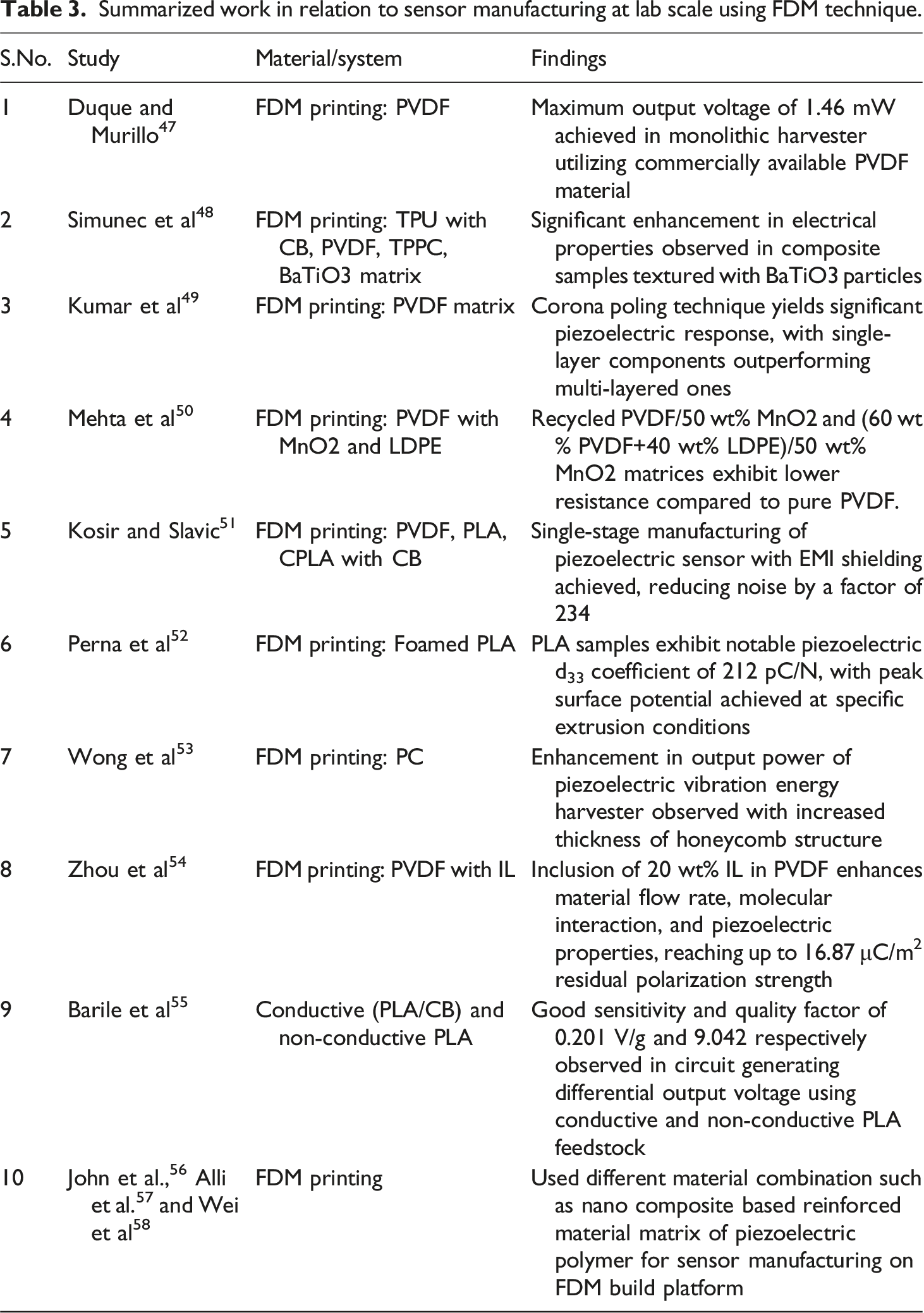
Figure 4 shows the (a) FDM printing of piezoelectric material matrix, (b) printed texture, (c) folded structure (Reused with permission of Simunec et al.
48
) and (d) Single stage FDM printed piezoelectric force measurement sensor (Reused with permission of Simunec et al.
51
; Creative Commons CC-BY).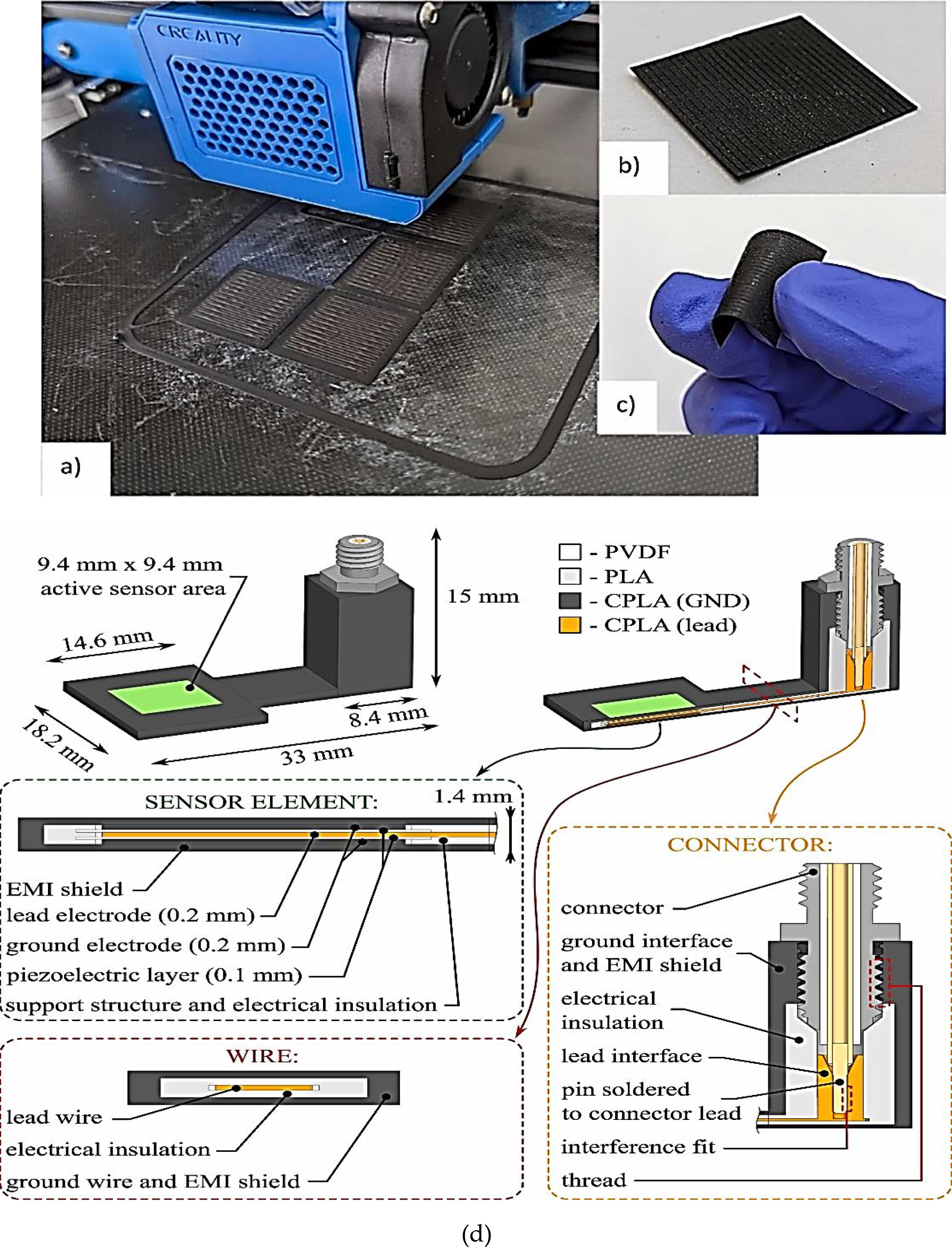
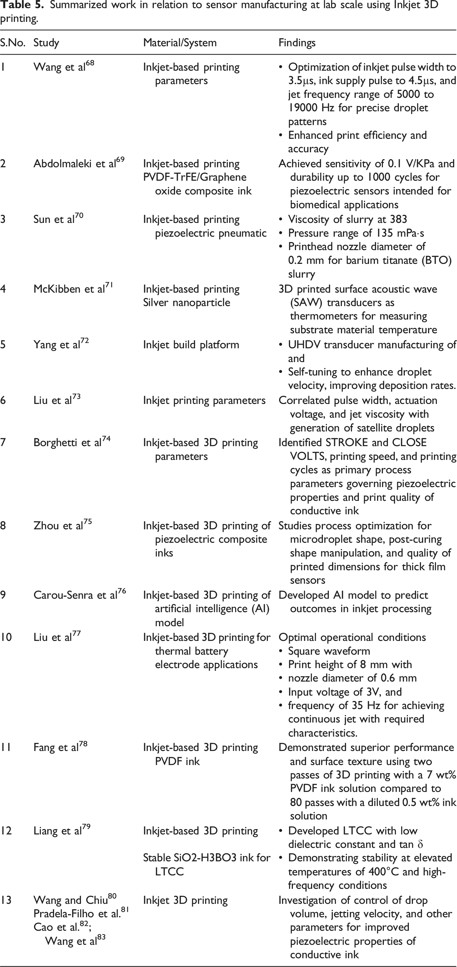
DIW based electroactive polymer printing
Direct Ink Writing (DIW) represents a novel methodology leveraging liquid inks, which are dispensed through fine nozzles in a controlled manner via pneumatic pressure or similar mechanisms. This automated system facilitates precise deposition of material onto a designated platform, conforming to user-defined parameters akin to established 3D printing software protocols. The intrinsic advantage of DIW resides in its adaptability to diverse ink formulations tailored to desired properties and functionalities.
Numerous scientific inquiries have delved into the utilization of DIW for printing electroactive materials, particularly to meet flexible and bespoke product requisites. In a seminal work by He et al., 59 a polyvinylidene fluoride (PVDF) matrix was meticulously engineered to modulate internal porosities, accommodating the incorporation of zinc oxide nanorods (ZnO-nr) to enhance piezoelectric responsiveness. This investigation underscores the efficacy of DIW in fabricating β-PVDF reservoirs with augmented surface energy, facilitating superior adhesion of ZnO-nr. Notably, the experimental findings revealed a notable enhancement, with PVDF micropores laden with ZnO-nr material yielding an output voltage of 33.2 V, marking a 2.36-fold improvement over conventional PVDF/piezoceramic-based energy harvesters. Liu et al. 60 delved into the development of Direct Ink Writing (DIW) ink utilizing waterborne polyurethane (WPU), barium titanate (BTO), and cellulose nanofibers (CNF) for applications in energy harvesting devices. The investigation yielded notable findings, showcasing a remarkable 70% compression recovery rate alongside a high relative sensitivity of 9.83 mV/kPa*wt%.
Yang and colleagues 61 conducted an inquiry into the utilization of barium titanate (BTO) nanoparticles in conjunction with bioactive glass (BG) across varying proportions for bone regenerative purposes. Their investigation unveiled the pivotal role of piezoelectric attributes in bone regeneration. Notably, the composite formulation of BTO/15 wt% BG ink bound with polyvinyl pyrrolidone (PVP) emerged as the optimal ratio for scaffold fabrication via 3D printing.
Scheper and Hunt 62 investigated an innovative strategy for DIW, integrating an airbrush alongside the writing nozzle to disperse nano-ink onto the 3D-printed surface during the printing process. Their exploration underscored the efficacy of this proposed technique in the 3D printing of cantilever beams composed of poly (vinylidene fluoride-trifluoroethylene-chlorotrifluoroethylene) (PVDF-TrFE-CTFE) as an electroactive polymer and carbon black (CB) as the electrode material. Notably, the quasi-static displacement (179 µm) and resonant displacement (2 mm) exhibited enhancements of 51% and 21%, respectively, for the performance of single and dual-layer electroactive polymer actuators.
Hill et al. 63 conducted an inquiry into the properties of poly(3,4-ethylenedioxythiophene): poly (styrene sulfonate) (PEDOT: PSS) as a conductive ink for forming intricate 3D structures. Their investigation aimed to elucidate the impact of various parameters on the conductivity of these 3D structures compared to their 2D film counterparts. The research successfully enhanced the conductivity to a remarkable 1200S/cm, surpassing that of 2D thin film configurations. The methodology involved the fabrication of the ink using spin coating or drop casting techniques, followed by the utilization of a piston-based deposition system for direct ink writing (DIW), replacing the conventional pneumatic printing approach.
Ghaderi et al.
64
explored PEDOT: PSS using co solvent and post solvent technique for ink preparation varying different solvents to examine the impact on resolution and conductive properties. A comparable investigation undertaken by Ma et al.
65
employed an 8 wt% carbon black (CB), carbon nanotube (CNT), and graphene multilayered powder composite, with a CB: CNT/GP ratio of 1:1 selected as the optimized blend for the formulation of conductive ink. Their findings propose that sensors fabricated using this composite ink ratio demonstrate a temperature sensitivity of 0.172/°C and enhanced cyclic loading and unloading characteristics. Zhao et al.
66
fabricated thin and thick film strain gauges employing platinum-rhodium (Pt-Rh) conductive ink on an aluminum substrate, capable of withstanding high temperature environments up to 1100°C utilizing the Direct Ink Writing (DIW) technique. Their investigation revealed the consistent functionality of the prepared thin film strain gauge under high-temperature conditions, exhibiting a gauge factor of 1.58, and a gauge factor of 2.42 at room temperature. Chen et al.
67
investigated voxel structure for conductive and piezoelectric ink with DIW build platform, which improved the output voltage and current of multi material 3D printed specimen to 150V and 16 µA respectively. Figure 5 shows the (a) different stages of DIW based nano ink coating technique with modified setup (Reused with permission of Scheper and Hunt
62
; Creative Commons CC-BY license); (b) ink preparation route and tactile sensor manufacturing using conductive ink (Reused with permission of Scheper and Hunt
65
; Creative Commons CC-BY license). Table 4 shows the summarized work of electroactive material work using DIW technique. (a) DIW based printing assisted with sprinkle base technique (Reused with permission of Scheper and Hunt
62
; Creative Commons CC-BY license); (b) ink preparation route for DIW and tactile sensor manufacturing using conductive ink of CB: CNT/GP in 1:1 ratio (Reused with permission of Scheper and Hunt
65
; Creative Commons CC-BY license). Summarized work in relation to sensor manufacturing at lab scale using DIW technique.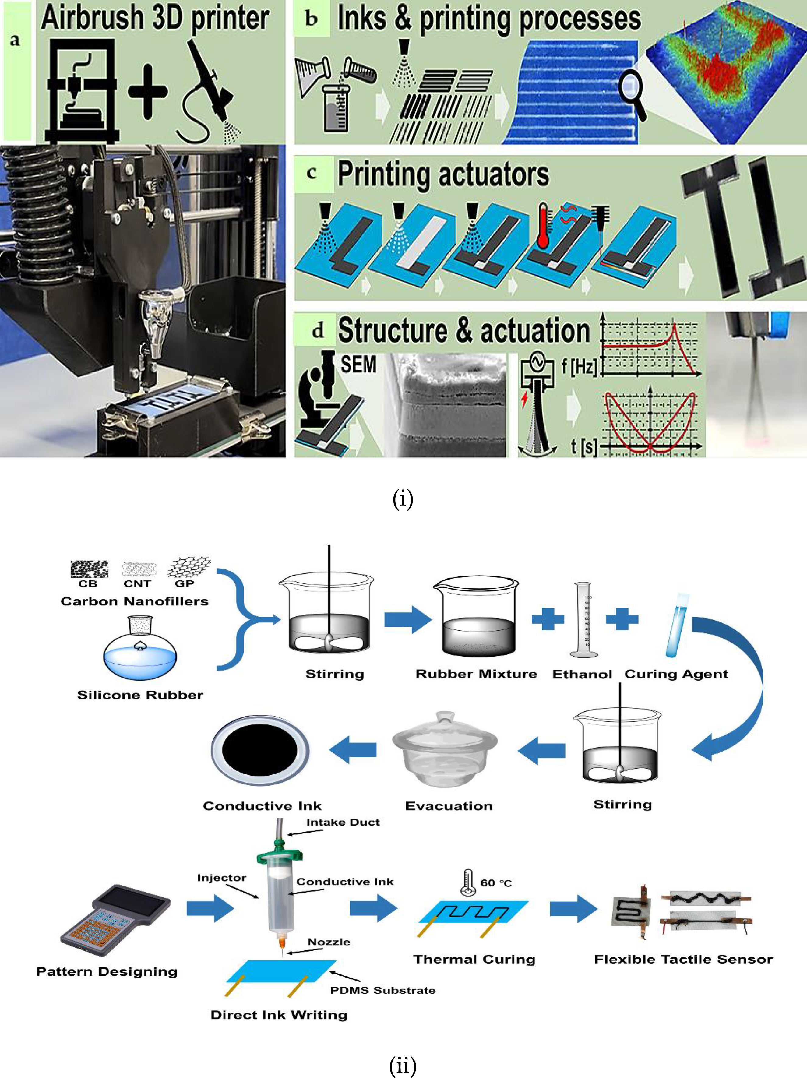
Inkjet based electroactive polymer 3d printing
Further in 3D printing of piezoelectric devices inkjet-based printing is one of the hot areas of research due to its flexibility in material exploration and capacity to build 3D and 2D films for sensor applications with fast processing, low cost and high surface area. The technique uses piezoelectric tubes to dispense the ink material on the substrate. The printers are capable of controlling the initial voltage and frequency to generate pressure to produce drops of ink that needs to be deposited over the substrate. The material gets dispensed over the build substrate with high frequency and accuracy. The printed material in 2D or 3D form is cured further using UV light exposure.
Many research studies exist today which have explored this technique varying the material combinations. Wang et al. 68 delved into an exhaustive examination of inkjet printing parameters concerning the intricate composition of piezoelectric material inks. Their meticulous scrutiny unveiled that the optimization of inkjet pulse width to 3.5µs, ink supply pulse to 4.5µs, and the maintenance of a jet frequency range spanning from 5000 to 19,000 Hz, conduced to the paramount conditions for achieving precise droplet patterns, thereby augmenting print efficiency and accuracy.
Abdolmaleki et al. 69 undertook research on PVDF-TrFE/Graphene oxide (GO) based composite ink for the manufacturing of piezoelectric sensors intended for biomedical applications. Their study yielded promising outcomes, demonstrating a sensitivity of 0.1 V/KPa and durability extending up to 1000 cycles. Sun et al. 70 delved into the exploration of piezoelectric pneumatic micro inkjet printing (PPMJ) for Barium Titanate (BTO) slurry, employing a composite ink combination containing 50 vol % BTO, varied dispersants. They observed that the viscosity of the slurry at 383, coupled with a pressure range of 135 mPa·s, utilizing a printhead nozzle diameter of 0.2 mm, constituted the optimized configuration for the PPMJ process.
McKibben et al. 71 embarked on an investigation involving silver nanoparticle ink deposition onto a piezoelectric substrate composed of LiNbO3 material matrix, aimed at fabricating surface acoustic wave (SAW) transducers. The prospective utility of inkjet-printed SAW transducers as thermometers for measuring substrate material temperature was elucidated. Yang et al. 72 scrutinized the ultrahigh dispersed velocity (UHDV) of ink on an inkjet build platform, coupled with self-tuning through positive crosstalk effects to enhance droplet velocity, thereby ultimately improving deposition rates. The study performed by Liu et al. 73 additionally correlated pulse width, actuation voltage, and jet viscosity as input parameters with the generation of satellite droplets. Similarly, Borghetti et al. 74 investigated inkjet printing parameters employing silver nanoparticle ink and Ti3C2TX, a member of the MXene family. Their study discerned STROKE and CLOSE VOLTS, printing speed, and printing cycles as the primary process parameters governing the piezoelectric properties and print quality of conductive ink.
Zhou et al. 75 have engaged in research involving various piezoelectric composite inks for the manufacturing of thick film sensors using piezoelectric pneumatic micro inkjet printing (PPMJ). Their investigation delved into the process intricacies concerning the control of microdroplet shape, post-curing shape manipulation, and the quality of printed dimensions. Carou-Senra et al. 76 pioneered the development of an artificial intelligence (AI) model to predict outcomes in inkjet processing. The model was trained using an in-house generated dataset encompassing pharmaceutical drugs, with diverse input process parameters such as nozzle diameter, supply voltage, drop spacing, and material-related attributes including consistency, surface tension, and composition.
Liu et al. 77 delved into the realm of inkjet printing for thermal battery electrode applications. Their study focused on identifying the optimal operational conditions to achieve the most efficient printing settings. Results indicated that employing a square waveform, a print height of 8 mm with a nozzle diameter of 0.6 mm, an input voltage of 3V, and a frequency of 35 Hz constituted the ideal configuration for attaining a continuous jet with the requisite set of characteristics. Fang et al. 78 have undertaken meticulous micro-patterning of a piezoelectric material (PVDF ink) for a nanogenerator tailored for 3D printing, mitigating the deleterious coffee ring effect and other anomalies. Their investigation delineated that employing two passes of 3D printing with a 7 wt% PVDF ink solution yielded superior performance and surface texture, in contrast to 80 passes with a diluted 0.5 wt% ink solution.
Liang et al.
79
investigated the printing process of a stable SiO2-H3BO3 ink to fabricate green samples of low-temperature co-fired ceramics (LTCC). The resulting specimens exhibited a low dielectric constant of 2.485 and tan δ of 0.0038. Furthermore, the developed LTCC green samples demonstrated stability at elevated temperatures up to 400°C and under high-frequency conditions. Many studies exist which have investigated process parameters of inkjet printing for improved piezoelectric properties of the used conductive ink (wang and Chiu
80
: investigated by controlling the drop volume and jetting velocity; Pradela‐Filho et al.
81
; cao et al.
82
; Wang et al.
83
). Figure 6 shows the (a) schema of inkjet printing for development of piezoelectric sensor (Reused with permission of Scheper and Hunt
68
Under a Creative Commons license CC BY-NC-ND 4.0). Table 5 shows the summarized work of electroactive material work using inkjet micro plotting/3D printing technique. Summarized work in relation to sensor manufacturing at lab scale using Inkjet 3D printing.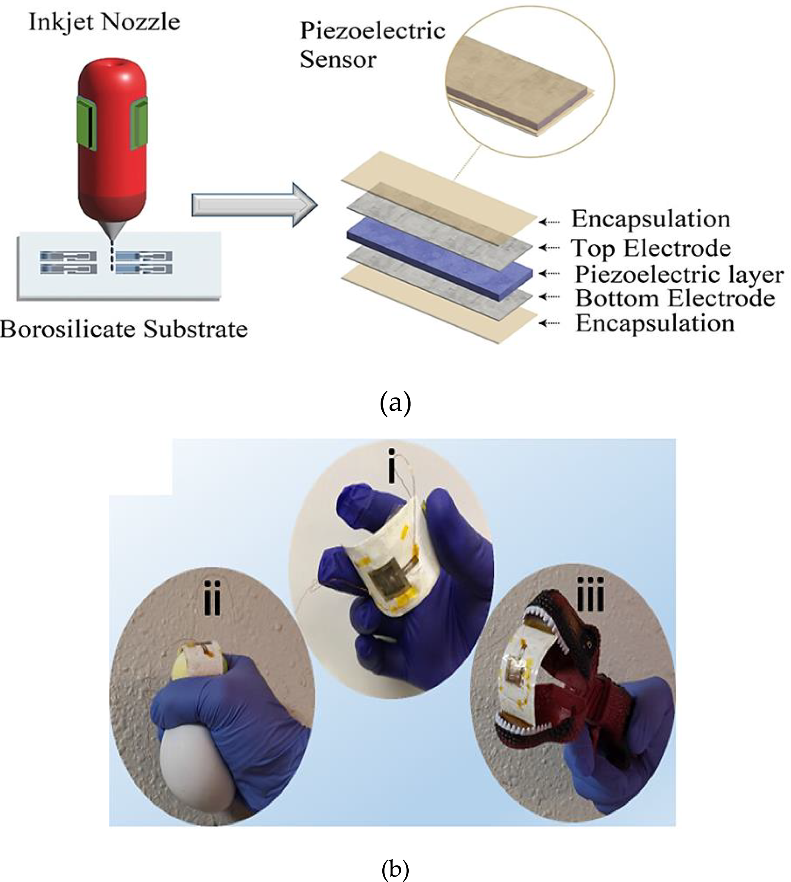
Overview of electroactive polymer synthesis and characterization using inkjet 3D printing route
Formulation strategy
Amidst the array of 3D printing methodologies capable of fabricating piezoelectric and electroactive material matrices, Inkjet printing utilizing microdroplets on demand emerges as a preeminent technique. Its proficiency lies in its capacity for flexible material composite generation while leveraging the entirety of 3D printing modules. Consequently, a meticulous examination of ink formulation and strategies is imperative, given the scarcity of studies delving into these aspects. The advent of novel ink composites holds paramount significance in the advancement of flexible electronic components, particularly in realms such as optoelectronics, wearable sensors, and biomedical sensors.
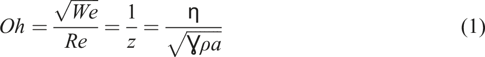
To comprehend the intricacies of ink formulation, one must grasp the fundamental constituents comprising ink structure, including particles, solvents, and surfactants. Crucial parameters governing ink behavior in inkjet printers encompass jettability, stability, resolution, and the uniformity of ink flow through nozzles, as elucidated by Derby et al.
84
Of particular relevance is the Ohnesorge (Oh) number, a dimensionless indicator pivotal in assessing ink jettability, ideally falling within the range of 1 to 10. This parameter stands reciprocally related to the Z-value, an indicator of ink jettability, and is intricately linked with the Weber number (We) and Reynolds number (Re), as depicted by equation (1).
85
Sajedi-Moghaddam and colleagues 86 employed particles within the range of 1/50 in size to mitigate the risk of nozzle clogging. Introduction of surfactants like sulfonyl 87 becomes imperative to optimize ink wettability, as excessively enhanced wettability may lead to diminished resolution. Moreover, achieving uniformity in printed structures may be compromised by the coffee ring effect, attributed to contact line pinning and capillary flow dynamics. 88 Addressing capillary flow requires inducing evaporation via surface tension gradients, a phenomenon known as Marangoni flow.89,90
Efforts to mitigate the coffee ring effect and enhance Marangoni flow involve incorporating co-solvents with high boiling points, such as diethylene glycol (DEG) and formamide (FA), alongside main solvents like water.91,92 Matavz et al. 93 delved into the formulation of Ta-Al-Si-alkoxide dielectric ink, utilizing 2-methoxyethanol as the main solvent (volatile, potentially inducing the coffee ring effect) and 1,3-propanol as a co-solvent liquid (highly viscous with optimal surface tension). In a separate study by Hu et al., 94 the efficacy of isopropanol (IPA) solvent was explored across various inks, including black phosphorus (BP), boron nitride (BN), and bismuth telluride (Be2Te3).
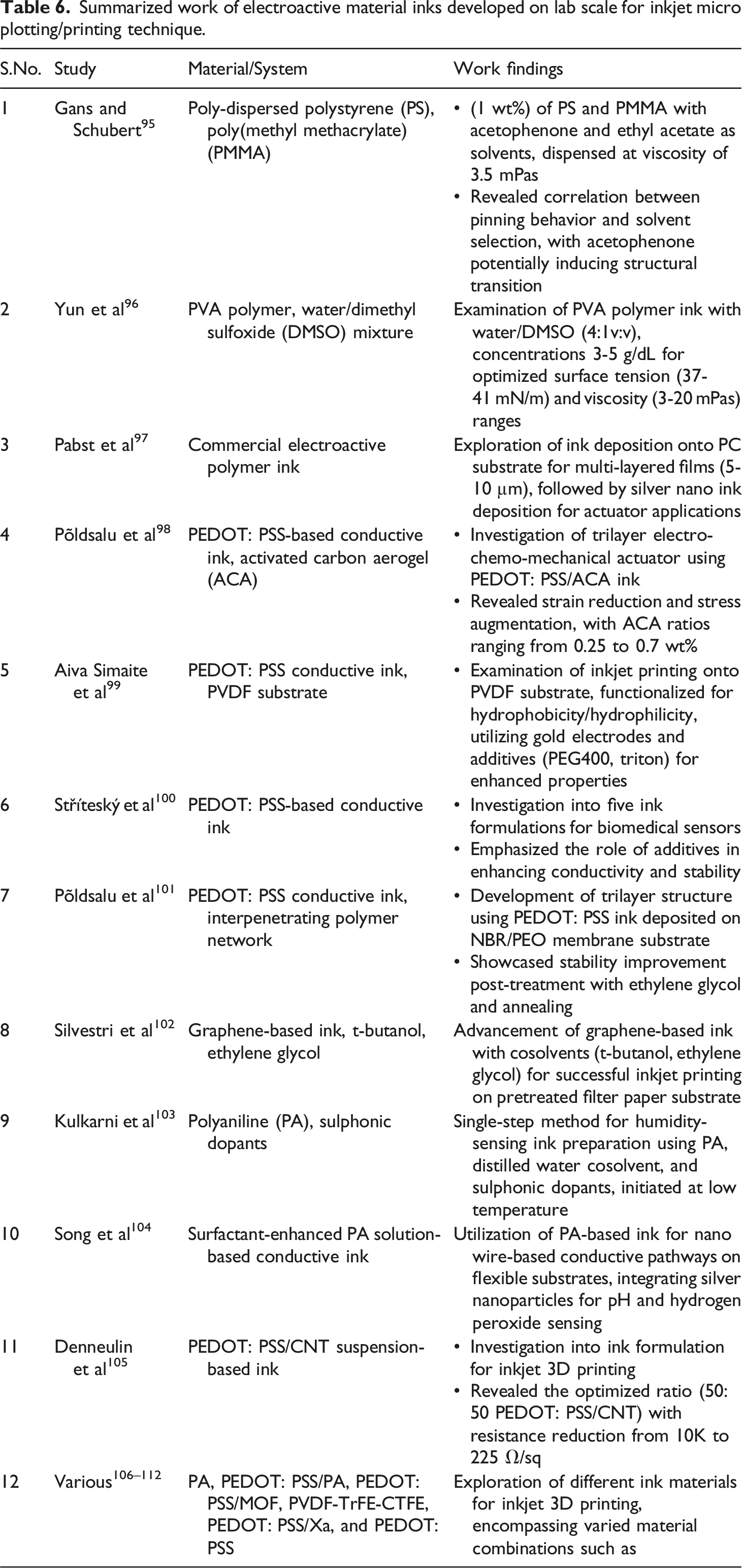
Historical overview for formulated inks on lab scale
The burgeoning demand for flexible electronics over the last decade has spurred the advancement of various composite, nanoparticle, and polymer inks exhibiting piezoelectric and electroactive properties. Gans and Schubert 95 scrutinized two distinct solutions: a 1 wt% solution of poly-dispersed polystyrene (PS) and a 1 wt% solution of poly(methyl methacrylate) (PMMA), each in tandem with acetophenone and ethyl acetate as solvents. The droplets were dispensed at a viscosity of 3.5 mPas, respectively. The investigation unveiled a discernible correlation between the pinning behavior and the structural attributes of the deposited droplet vis-à-vis the solvent selection. The introduction of acetophenone (10 wt%) into ethyl acetate was found to potentially induce a transition from a ring structure to a dot structure. Yun et al. 96 conducted an investigation into the utilization of PVA polymer in conjunction with a water/dimethyl sulfoxide (DMSO) mixture in a volumetric ratio of 4:1v:v, with concentrations ranging from 3 to 5 g/dL, as the optimized ink formulation. The optimized concentration and ratio exhibited a surface tension within the range of 37-41 mN/m, coupled with an optimal viscosity range of 3-20 mPas. Subsequently, Pabst et al. 97 delved into the exploration of commercially available electroactive polymer ink deposition onto a PC substrate for the fabrication of multi-layered films with a thickness ranging from 5 to 10 µm. Following the annealing process of the polymeric samples, silver nano ink was deposited utilizing inkjet printing techniques for potential actuator applications.
Põldsalu and colleagues 98 delved into the investigation of PEDOT: PSS-based conductive ink alongside activated carbon aerogel (ACA) for the development of a trilayer electro-chemo-mechanical actuator. The incorporation of ACA into the PEDOT: PSS matrix resulted in a reduction in strain and an augmentation of stress within the PEDOT: PSS/ACA structure. ACA was introduced at ratios ranging from 0.25 to 0.7 wt% relative to the PEDOT: PSS commercial ink, which possessed a solids content ranging from 0.6 to 1.2 wt%. The experimentation utilized PVDF as a substrate for the 3D printing of conductive ink, facilitating the exploration of the trilayer architecture. Similarly, Aiva Simaite et al. 99 examined the inkjet printing of PEDOT: PSS conductive ink onto a PVDF substrate that was functionalized to exhibit a hydrophobic upper surface and a hydrophilic center, achieved through grafting with polyethylene glycol methacrylate (PEGMA). To establish a circuit, gold electrodes were initially deposited onto a commercially available PVDF membrane substrate, followed by the deposition of PEDOT: PSS-based commercial ink (1.3 wt%). The researchers introduced poly(ethylene glycol) (PEG400) and triton as additives to the PEDOT: PSS-based ink to enhance its properties.
Stříteský et al. 100 conducted an investigation into five distinct formulations of PEDOT: PSS-based conductive ink aimed at fabricating a biomedical sensor. These inks were sourced commercially and varied in grade. Their research underscored the critical role of additives in ink composition, revealing that PEDOT: PSS ink synthesized at the laboratory scale without such additives exhibited inferior conductivity and stability. Furthermore, they achieved enhanced stability in 3D-printed microfilms through treatment with ethylene glycol followed by annealing.
In a related study, Põldsalu et al. 101 focused on developing a trilayer structure utilizing PEDOT: PSS conductive ink with a solid content ranging from 0.6% to 1.2% by weight. This involved depositing the ink onto a spin-coated substrate composed of an interpenetrating polymer network consisting of nitrile butadiene rubber (NBR) and a poly(ethylene oxide) (PEO) membrane. Silvestri et al. 102 undertook an investigation into the advancement of graphene-based ink for inkjet microprinting applications. Initially, the researchers synthesized electrochemically exfoliated graphene (EEG) and subsequently utilized t-butanol and ethylene glycol (each at a volume fraction of 10%) as cosolvents in the ink formulation to effectively lower the surface tension, thereby enabling successful inkjet printing. The substrate of choice for the ink was pretreated filter paper.
In a separate study, Kulkarni et al. 103 devised a single-step method for producing conducting ink composed of polyaniline (PA), utilizing sulphonic dopants tailored for humidity sensing applications. The ink preparation involved using distilled water as a cosolvent. The polymerization reaction was initiated by mixing a solution of PA containing 1.33 mg of sulphonic acid with Ammonium persulphate (1M) at a low temperature range of 0 °C–5 °C. Additionally, Song et al. 104 explored the utilization of surfactant-enhanced PA solution-based conductive ink for printing nano wire-based conductive pathways on flexible substrates, facilitating the fabrication of pH and hydrogen peroxide sensors by incorporating silver nanoparticles into the PA-based ink. The synthesis of PA nanowires involved separately preparing aniline in 1M HCl and ammonium peroxydisulfate (45 mg in 1M HCl), which were later combined at high speed.
Summarized work of electroactive material inks developed on lab scale for inkjet micro plotting/printing technique.
Summary and discussions
From the literature review of different 3D printing techniques used in flexible electronic application it has been ascertained that additive manufacturing techniques have revolutionized the fabrication of functional materials for diverse applications, particularly in the realms of electronics and biomedical engineering. The findings related to the SLA-based 3D printing has shown its edge in exploring and enhancing various materials' properties for specific applications. From investigating lead-free piezoceramics to synthesizing UV-curable pastes containing composites, each study delves into optimizing material compositions, printing techniques, and post-processing methods. Through meticulous experimentation, researchers have achieved remarkable advancements in piezoelectric, mechanical, and electrical properties, paving the way for innovative applications in fields such as ultrasonic transducers, electromechanical systems, and bioinspired structures. These findings collectively contribute to the growing body of knowledge in materials science and additive manufacturing, offering insights into the manipulation of material properties at the microstructural level for tailored functionalities and improved performance in various engineering applications. Further the SLA based 3D printing has some challenges or constraints due to the technique of printing. It requires photosensitive material that can be photon cured in presence of laser beam. Further, the material experiences shrinkage while getting solidified resulting in internal stresses in final product.
Thanks to developments in SLS 3D printing, composite materials have been the subject of revolutionary new developments. Researchers have investigated the possibility of improving the electrical, mechanical, and thermal characteristics of polymer matrices by including fillers such as graphene oxide (GO), carbon black (CB), and reduced graphene oxide (r-GO). Bone tissue engineering, electronics, and the creation of electric motors devoid of metal are just a few of the many potential areas that may benefit from these advancements. There are a lot of benefits to this method over the SLA-based approach, one of which is that it doesn’t need an addition of photosensitive material. In addition, the product’s properties may be customized by melting the polymeric powder with different reinforcements, depending on what the customer needs. In addition to its benefits, the technology is not without its drawbacks. These include a porous structure, 113 high internal stress, 114 the impact of shrinkage and warping115,116 caused by the high energy density of the laser beam, and the solidification phenomena of the melted pool.
Much progress and new understanding have resulted from investigating FDM in the context of piezoelectric sensor production. Exploring new methods like contact and corona poling, as well as utilizing PVDF, TPU, and PLA as composite matrices with fillers like carbon black, graphene, and BaTiO3, researchers have revealed a wide range of opportunities for improving mechanical and electrical properties. Further, research has shed light on the complex interplay between raw material properties, processing factors, and final performance measures, providing useful direction for ongoing and future projects in this area. Warping, a choked nozzle, and post-processing needs such support structure removal and surface polishing are just a few of the difficulties that might arise from using this printing method. The method has been seeking industry adoption for the development of finished/ready-to-use products despite its adaptability and flexibility in using a variety of materials on its platform.
The literature survey on DIW has demonstrated its flexibility in fabricating intricate structures with enhanced properties for a range of purposes, including energy harvesting, bone regeneration, actuator fabrication, conductivity enhancement, sensor development, and strain gauge production. Key findings include significant improvements in voltage output, compression recovery rate, conductivity, temperature sensitivity, cyclic loading characteristics, and strain gauge functionality. Moreover, innovative techniques such as integrating an airbrush with the writing nozzle and exploring voxel structures for conductive and piezoelectric ink demonstrate promising avenues for further advancement in DIW technology. The challenge related to the DIW technique is in development of ink to be used on its platform. The material viscosity is the most crucial parameter which decides the thixotropic nature of material. The ink viscosity and modulus should be less while printing stage when shear is high and should reach to its original value once shear stops. Printer nozzle clogging and air bubble entrapment are some of the other issues which must be taken care by the user.
Comparative conclusion for various additive manufacturing techniques in sensor development.
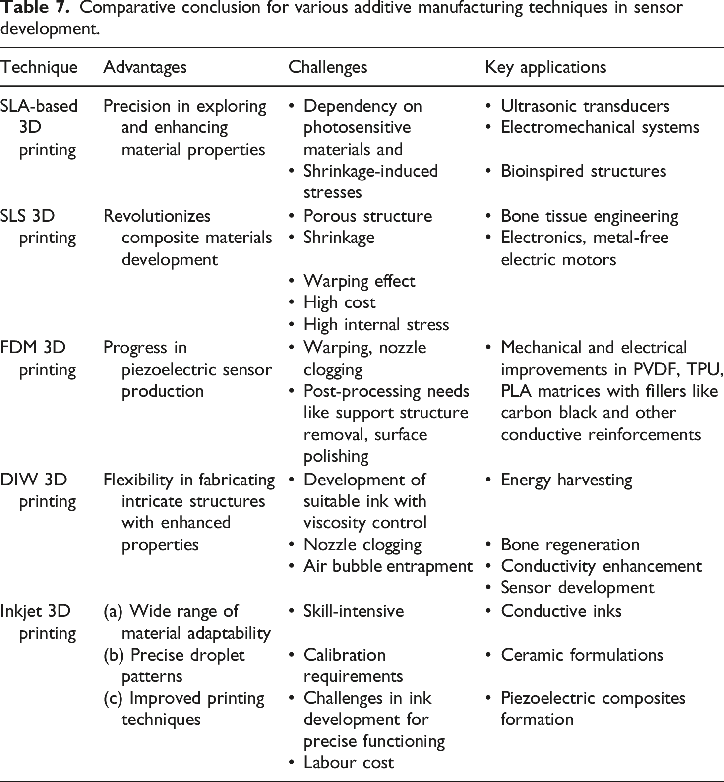
Further many studies exist which have developed polymeric composite matrix for different type of sensors.117,118 Many research findings have reviewed and worked for the development of smart material matrixes.119,120 In conclusion, the review underscores the transformative impact of additive manufacturing techniques, particularly Stereolithography (SLA), Selective Laser Sintering (SLS), Fused Deposition Modeling (FDM), Direct Ink Writing (DIW), and inkjet-based printing, in revolutionizing the fabrication of flexible electronic materials. These technologies offer unparalleled versatility, precision, and customization, paving the way for groundbreaking advancements in electronics, biomedical engineering, and beyond. Moving forward, further research endeavors must continue to explore the frontiers of material science, customization methodologies, and optimization strategies to unlock the full potential of these additive manufacturing techniques. This shift towards more efficient and cost-effective solutions will not only revolutionize industries, but also improve the quality of life for individuals worldwide. It is imperative that researchers and industry leaders collaborate to push the boundaries of additive manufacturing and bring about a new era of technological innovation. Different additive manufacturing technique has its advantages and disadvantages in relation to particular application. The choice of selection of technique for piezoelectric sensor development depends over the different parameters such as flexibility requirement, cost involvement, sensitivity requirement and accuracy of the product. As per the reported literature inkjet-based 3D printing offers flexibility (in relation to material choice such as flexible materials such as TPU, polyurethane, polyimide and other materials) accuracy (resolution, sensitivity, life cycle of sensor) thus it may be considered as suitable technique for fabrication of flexible piezoelectric sensors.
Research gap and future direction
Recent developments in sensor manufacturing have seen extensive interest of research community for inhouse development of sensor and its application for industry. But the constraints of the techniques have resulted in less industrial adoption of in-house developed sensors. Further research should focus on the development and optimization of novel materials suitable for each 3D printing technique. This includes exploring new composite materials with enhanced electrical, mechanical, and thermal properties, as well as tailoring material compositions to specific application requirements. For further material development flexible polymeric material matrix such as TPU, polyurethane, polyimide etc can be reinforced with conductive materials such as CNT, graphene, BaTiO3, reduced graphene oxide (rGO) material by controlling viscosity, thixotropic nature, shear resistance, surface tension etc. Continuous efforts should be made to improve the 3D printing processes themselves, aiming to overcome existing challenges and limitations by developing hybrid processes of sensor development. This could involve refining printing parameters, developing innovative printing strategies, and addressing issues such as shrinkage, warping, nozzle clogging, and internal stresses. Utilizing artificial intelligence (AI) and machine learning algorithms can enhance the predictive capabilities of 3D printing processes. By leveraging AI models, researchers can optimize printing parameters, forecast outcomes, and mitigate printing anomalies, leading to more efficient and reliable manufacturing processes. Research into advanced post-processing techniques can further enhance the properties and performance of printed objects. This includes methods for surface finishing, structural reinforcement, and surface modification to improve durability, functionality, and overall quality. Emphasizing the customization and personalization capabilities of additive manufacturing for flexible electronics can open up new opportunities in various industries. By tailoring designs and material properties to individual requirements, additive manufacturing can offer unique solutions for specific applications, such as medical devices, wearable electronics, and consumer products. Efforts should be directed towards scaling up additive manufacturing processes for mass production and promoting their widespread industrial adoption. This involves addressing issues related to scalability, repeatability, cost-effectiveness, and regulatory compliance to facilitate the transition from prototyping to full-scale production.
Footnotes
Acknowledgements
The authors are highly thankful towards the Thapar Institute of Engineering and technology for their continuous motivational and technical support.
Declaration of conflicting interests
The author(s) declared no potential conflicts of interest with respect to the research, authorship, and/or publication of this article.
Funding
The author(s) disclosed receipt of the following financial support for the research, authorship, and/or publication of this article: The authors would like to acknowledge the funding received from Indian government DST sponsored project file number DST/TDT/AM/2022/365 for preparation and other work related to this manuscript.