
Abstract
To address the critical challenge of thermo-mechanical stress in large-area thin-film transistor fan-out panel-level packaging (TFT-FOPLP), this study employs a finite-element modeling to investigate stress distribution from the panel to the device scale. A hierarchical sub-modeling methodology was used, starting with a homogenized global model to identify high-stress regions, followed by two levels of sub-models to resolve stresses in a single TFT cell under simulated thermal cool-down from fabrication temperatures. Results identified the highest stress concentrations at the corners of dies near the panel edge. At the device level, the analysis revealed that the critical gate insulator is subjected to a tensile stress of approximately 44.5 MPa and a strain of about 0.1%, a level sufficient to potentially alter electrical performance. Furthermore, other brittle dielectric layers, such as the passivation layer, were predicted to experience significantly higher stresses (approximately 407 MPa), indicating a primary risk of mechanical fracture. The study affirms the mechanical feasibility of the TFT-FOPLP concept but underscores the need for careful stress mitigation in vulnerable regions. The presented modeling framework provides a powerful tool for design-for-reliability by enabling the early prediction of high-stress zones, thereby reducing reliance on physical prototyping. Future work should focus on correlating these simulations with experimental electrical data to establish quantitative design rules for this promising technology.
Keywords
Introduction
The advancement of the semiconductor industry has long been propelled by device scaling, as articulated by Moore's law.1–6 As further miniaturization became increasingly complex, the strategic focus precipitated a paradigm shift toward More-than-Moore integration, which prioritizes novel functionalities and heterogeneous system integration at the packaging level over pure transistor scaling. 7 Consequently, fan-out panel-level packaging (FOPLP) emerged as a leading methodology, enabling high-density device integration on large-area substrates to improve manufacturing throughput and reduce cost.8–10 While economic studies confirm its cost advantages, 9 significant hurdles such as panel warpage and yield loss remain critical challenges for the industry.10,11 This study focuses on an advanced architecture, thin-film transistor-based FOPLP (TFT-FOPLP), which integrates active devices directly into the packaging architecture.12,13 This strategy allows for the migration of functional blocks like display drivers and sensors from the silicon die to the panel substrate, facilitating a reduction in silicon area. 14 A thin-film transistor, the core of this technology, is a semiconductor device that functions as an electrical switch.15,16 For this work, low-temperature polycrystalline silicon (LTPS) TFTs were selected due to their high carrier mobility and established use in display manufacturing, making them ideal for high-performance circuitry within the FOPLP structure.17–19
However, a critical challenge in large-area FOPLP is the management of thermo-mechanical stress, which arises primarily from coefficient of thermal expansion (CTE) mismatches during the thermal cycles of fabrication. 19 These stresses drive phenomena like warpage and delamination and directly induce strain in the embedded TFTs, leading to performance degradation.20–24 The current state of research in this area reveals a significant gap. Existing thermo-mechanical simulations for FOPLP predominantly focus on predicting global warpage using homogenized models, which are incapable of resolving device-level features.25,26 Concurrently, separate and extensive studies have confirmed that the electrical behavior of LTPS TFTs is highly sensitive to mechanical strain, which can cause threshold voltage shifts and degrade carrier mobility.17,27–32 This degradation is known to be accelerated by combined thermal and mechanical loads, highlighting the urgent need for accurate stress analysis. 33
Despite this, a comprehensive model that directly links macro-scale manufacturing stresses to the micro-scale integrity of embedded active devices has been a notable gap in the literature. 31 This study bridges this critical gap by implementing a hierarchical, global-to-local modeling strategy for the detailed thermo-mechanical analysis of an active TFT-FOPLP system.34–36 The primary novelty of this work is the application of this hierarchical, multi-scale finite-element modeling framework to such a structure. To the best of the authors’ knowledge, this is the first comprehensive investigation to apply this methodology to a TFT-FOPLP system. Our approach systematically connects the global deformation of the entire panel to the localized stress within a single TFT cell. 34 This framework enables the accurate prediction of stress concentrations in vulnerable device layers, such as the gate insulator (GI), arising from global process-induced loads. 35 By doing so, our work provides a powerful predictive tool for design-for-reliability, enabling the early identification of high-stress zones and reducing reliance on costly physical prototyping. 26
Methodology
The thermo-mechanical simulation framework presented in this study is built upon several well-established finite-element analysis techniques that are standard in the field of electronics packaging. These foundational methods include the use of a coarse, global model for initial warpage and stress assessment; the homogenization of complex composite layers to maintain computational efficiency; the application of the general global-to-local sub-modeling principle to analyze localized stress concentrations; and the simplification of the complex thermal history into an equivalent thermal load case. The primary novelty of this work, however, lies not in the invention of these individual techniques, but in their specific integration and application to create a seamless, multi-scale framework uniquely tailored for an active TFT-FOPLP system. While sub-modeling is a known method, the design of our particular two-level hierarchy (Global Model ⇒ Package-Scale SM1 ⇒ Device-Scale SM2) is a new approach developed for this problem, custom-built to manage the vast difference in length scales. To our knowledge, this work represents the first application of such a framework to systematically and quantitatively bridge the analytical gap between macro-scale panel deformation and the micro-scale stress induced within a single, active transistor in an FOPLP architecture. Our methodology was specifically designed to create a direct analytical link between two previously separate domains of study: panel-level manufacturing stress and the strain effects on individual TFT device integrity. This section details the implementation of this framework. First, the overall modeling approach, layer structure, and material properties are described. Next, the thermal load simulation is explained. Finally, the hierarchical global-to-local sub-modeling technique, which enables an efficient yet accurate stress analysis, is presented.
Mechanical modeling approach
The approach adopted for the panel-level analysis detailed in this study is fundamentally consistent with the established and widely accepted practices for the thermo-mechanical simulation of large-area electronic packages. The idealization of the global model employs several conventional techniques to ensure a robust and computationally efficient foundation for the subsequent sub-modeling stages. Specifically, these include: the use of a quarter-symmetry model to leverage the panel's geometric and loading symmetry; the assumption of linear elastic material behavior for a first-order assessment of stress distribution; and the simplification of the complex fabrication thermal history into an equivalent thermal load case, as will be explained in the section “Thermal process simulation.”
Furthermore, the treatment of complex composite layers through material homogenization is a standard and necessary technique for macro-scale analysis, and the method for calculating these effective properties for our unique structure is detailed in the section “Layer structure and materials.” Therefore, no fundamental changes were made to these established modeling methods. The primary adaptation for this study was the rigorous application of these techniques to the novel TFT-FOPLP architecture. This required the specific and detailed characterization of its unique multi-layer material stack to ensure the global model, which serves as the foundation for the entire hierarchical analysis, was both reliable and accurate.
Finite-element modeling was performed to simulate the thermo-mechanical behavior of the TFT-FOPLP package structure during a representative thermal process cycle. The simulation focused on thermal stress induced by temperature variations, specifically the cooling phase as the structure transitions from high processing temperatures down to room temperature. This cooling process generates stress due to mismatches in CTEs among different materials.
To reduce computational cost, a quarter-symmetry model of the panel was constructed, leveraging geometric symmetry along both the X and Y directions. Symmetry boundary conditions were imposed on the planes where X equals zero and Y equals zero, by constraining normal displacement along those surfaces. The analysis was carried out in multiple stages. It began with a coarse global model of the entire panel to evaluate overall warpage and bulk stress distribution. This was followed by detailed local sub-models that provided higher resolution in areas identified as critical. All simulations assumed that materials behaved in a linear elastic manner and the focus was placed on evaluating elastic stresses and strains present after the structure had cooled.
Layer structure and materials
A TFT-FOPLP has a multi-layer structure typical of advanced packages. As shown in Figure 1(b), the layer stack is built on a glass substrate. This substrate supports several layers, including copper redistribution layers (RDLs), polymer dielectric films (e.g. D1), solder bumps, and an epoxy mold compound (EMC). A silicon die is mounted at the center of each package and connected to the RDL through an array of solder bumps. A key feature of this design is the dedicated TFT layer built on a polymer interposer. The properties of the main materials in the package are listed in Table 1. The glass panel has a thickness of 0.7 mm, a Young's modulus of about 73 GPa, and a CTE of about 3.8 ppm/°C. A photosensitive polyimide (PI) is applied to the glass, acting as a stress buffer and carrier for the TFTs. The copper RDLs fan out the die pads to a larger pitch and are insulated by dielectric films. Connection between the die and RDL is made using tin–silver (Sn–Ag) solder bumps and under bump metallurgy layers. The structure is encapsulated by an EMC for structural support and protection.
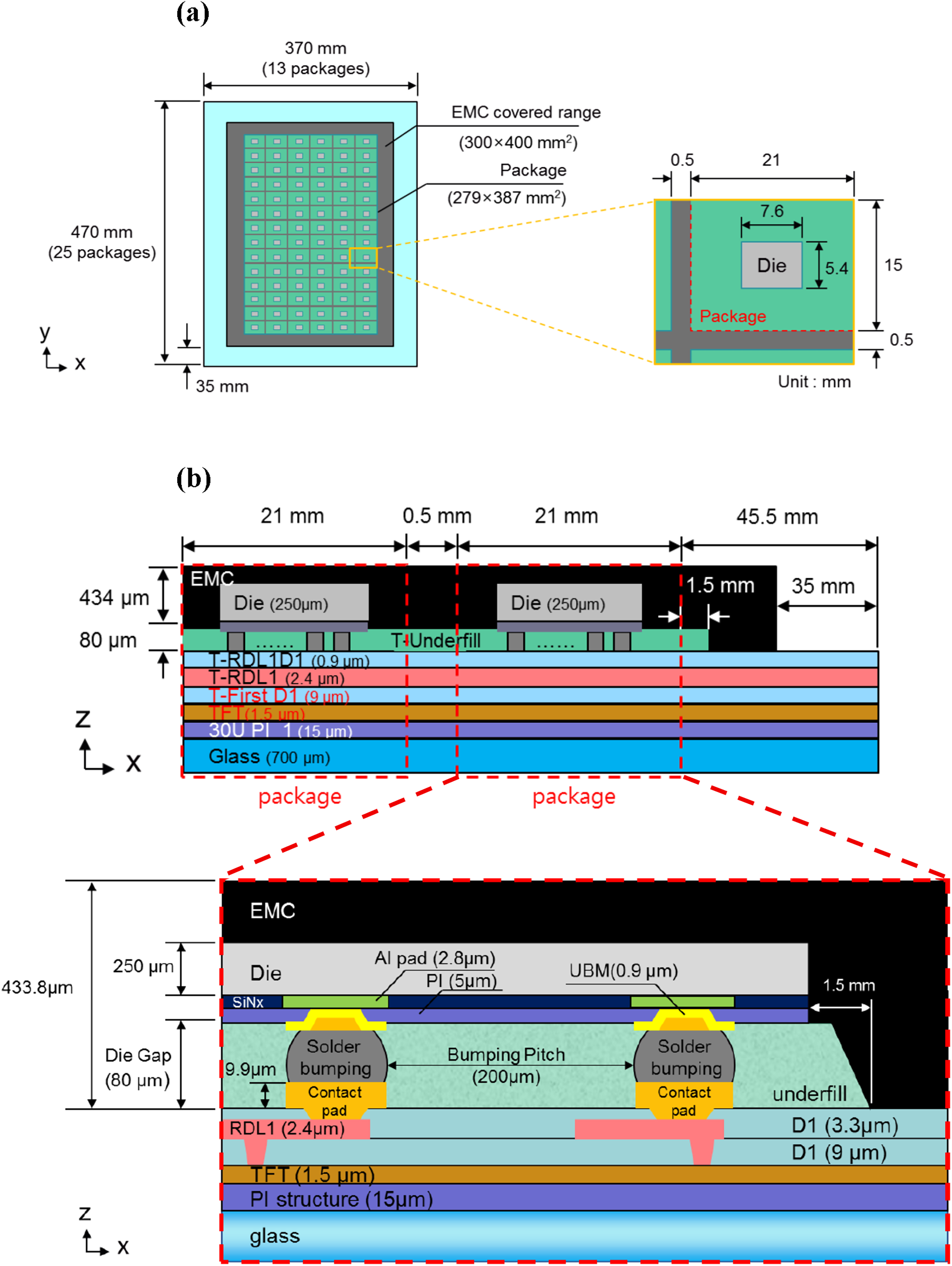
An overview of the TFT-FOPLP package structure: (a) top view and (b) detailed cross-sectional view. TFT-FOPLP: thin-film transistor fan-out panel-level packaging.
Mechanical properties of TFT-FOPLP package materials.
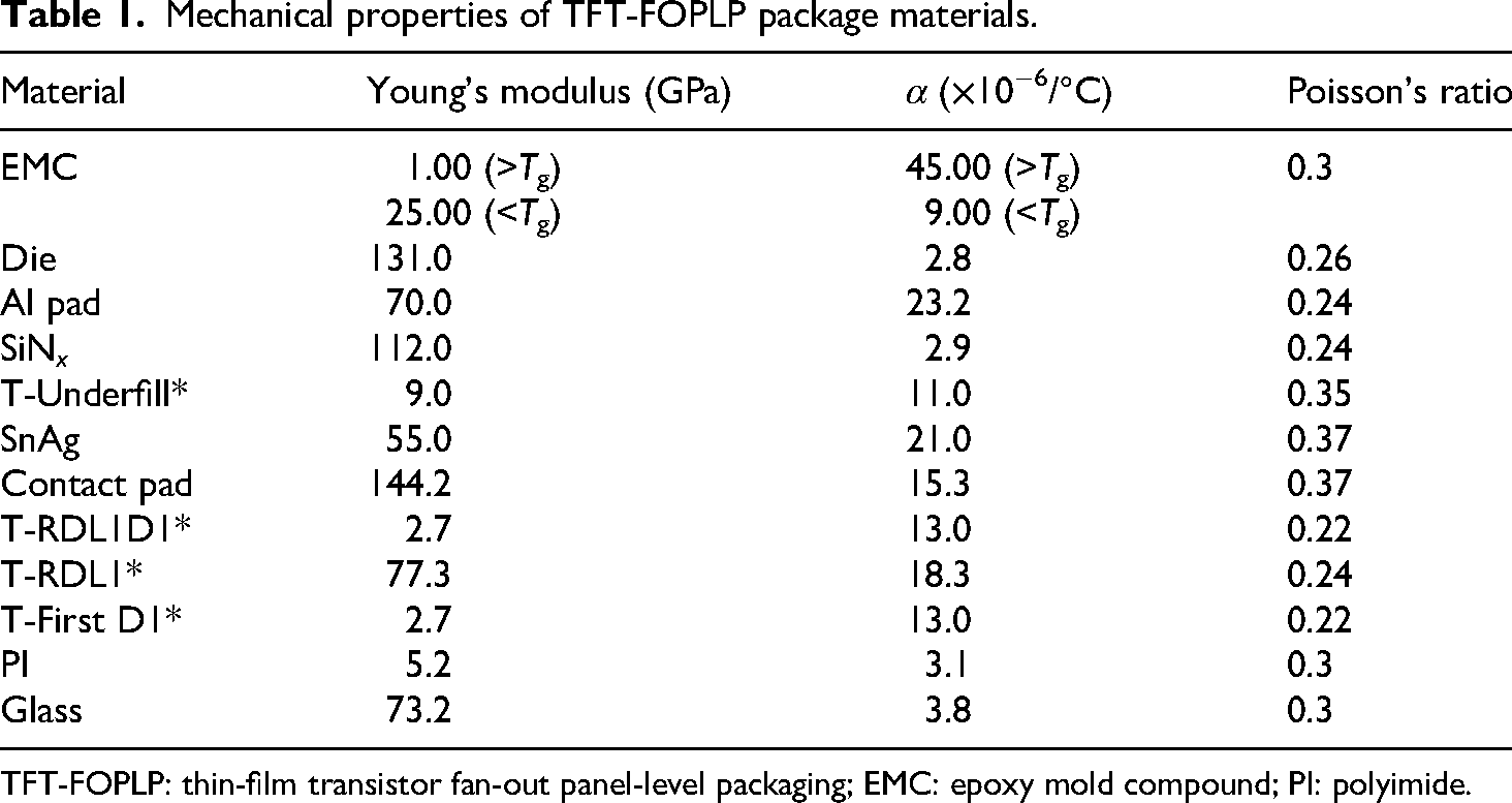
TFT-FOPLP: thin-film transistor fan-out panel-level packaging; EMC: epoxy mold compound; PI: polyimide.
To simplify the analysis, complex composite layers in the model were homogenized. This process improves computational efficiency. For example, layers with mixed structures, such as the RDL with its dielectric or the underfill with its array of bumps, were treated as single materials with equivalent properties. These equivalent properties were calculated using the rule of mixtures (marked by an asterisk * in Table 1)34–36:


In the simulation, all materials are treated as linear elastic. Most materials are considered isotropic, but the homogenized layers are treated as orthotropic to account for their directional structure. The EMC's properties are temperature-dependent, based on its glass transition temperature (Tg) of 148 °C. Above this temperature, the EMC's modulus drops significantly from 25 to 1 GPa, while its CTE increases from 9 to 45 ppm/°C, as shown in Table 1.
TFT cell structure
The active layer of the panel consists of an array of TFTs, which are the focus of the detailed local-level analysis. The planar layout of a representative unit cell is shown in Figure 2(a), its schematic cross-section is provided in Figure 2(b), and a micro-graph of the actual fabricated cell is presented in Figure 3 for physical reference. The selected sub-model for this analysis represents a polysilicon (poly-Si) TFT with a channel width (W) and length (L) of 8 μm each. As depicted in the cross-sectional schematic, the device architecture comprises a complex multi-layered stack constructed upon a poly-Si active island. The gate electrode (M1) is patterned over the poly-Si, electrically isolated by a GI and a silicon nitride (SiN x ) layer. In a superior layer, the source and drain electrodes (M2) make contact with the underlying poly-Si active region through metallic vias. A third metal layer (M3) is subsequently integrated within the first RDL. Functionally, the device's conductive channel forms within the poly-Si layer at the interface with the GI upon the application of a gate voltage.
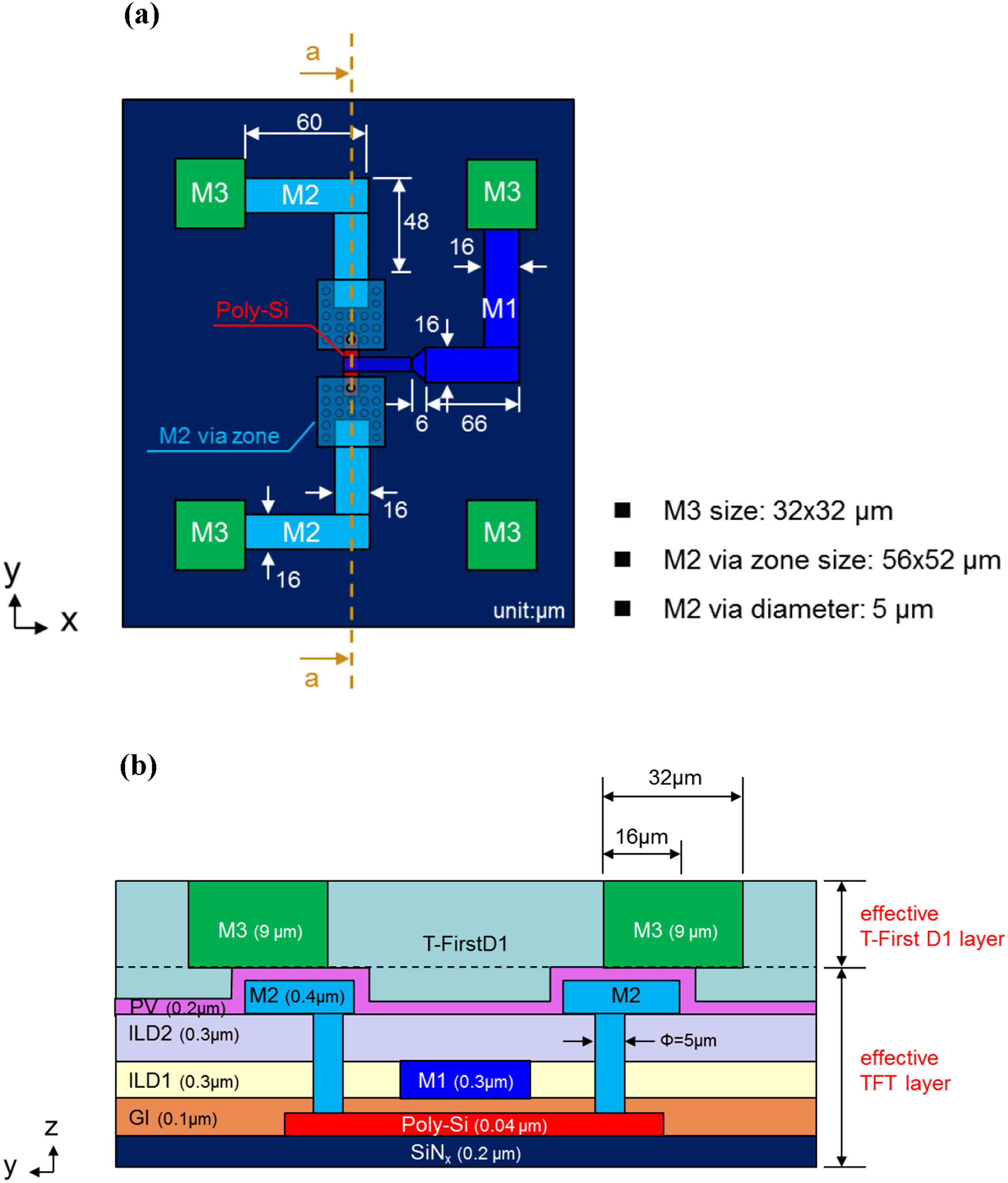
TFT cell geometry: (a) top view and (b) cross-section a-a.

Image of the fabricated TFT cell layout. TFT: thin-film transistor.
For the global-scale model, where analyzing each individual transistor is computationally prohibitive, the active layer containing this complex TFT array is instead abstracted as a single, homogeneous material with effective orthotropic properties. This homogenization is a standard technique used to account for the layer's aggregate contribution to the overall package stiffness while maintaining computational efficiency. The equivalent elastic properties for this layer, enumerated in Table 2, were determined through detailed material characterization. The in-plane Young's modulus (Ex = Ey) is approximately 158.7 GPa, a value significantly elevated by the high modulus of the embedded metallic interconnects, while the out-of-plane modulus (Ez) is 120.2 GPa. The layer's effective CTE is approximately 7.26 ppm/°C in-plane and 9.82 ppm/°C in the through-thickness direction, with a Poisson's ratio of about 0.35. While this homogenized approach is suitable for global-level analysis, it cannot resolve stresses within the micro-scale features of an individual transistor, which necessitates the detailed local sub-model.
Equivalent orthotropic properties of the composite TFT layer.
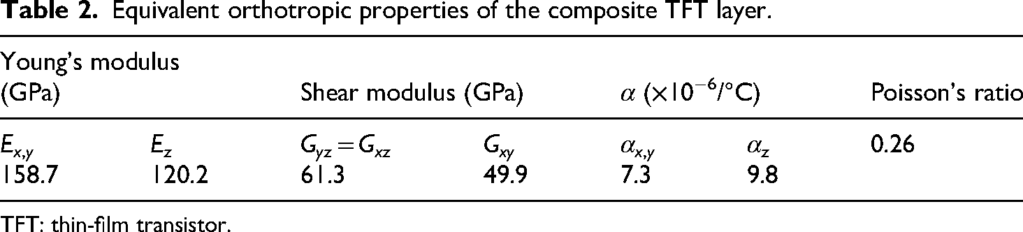
TFT: thin-film transistor.
The material properties for the constituent layers of the TFT cell are detailed in Table 3. These properties encompass the metallic layers (M1, M2, M3), typically copper with a Young's modulus of approximately 119 GPa; the poly-Si active layer (E: about 160 GPa, CTE: about 2.8 ppm/°C); and various dielectric materials, including SiO2 and SiN x , which exhibit moduli ranging from 85 to 288 GPa.
Material properties of TFT cell constituent layers.

TFT: thin-film transistor.
From a mechanical reliability standpoint, the TFT cell is a vulnerable structure. The juxtaposition of stiff, brittle dielectric materials (i.e. SiN x , SiO x ) with other layers creates a high risk of fracture when subjected to tensile stress. Consequently, the accurate prediction of the maximum principal stress within these brittle layers is paramount for assessing the thermo-mechanical reliability of the device.
Thermal process simulation
The focus of this thermo-mechanical simulation is the sequence of thermal excursions experienced by the panel during its multi-stage fabrication process. The manufacturing sequence involves numerous thermal cycles, including, for example: the curing of PI at approximately 450 °C; the deposition of the TFT layer via laser crystallization at roughly 150 °C; the curing of dielectric films for the RDL at approximately 250 °C; flip-chip die attach involving a solder reflow process peaking at about 230 °C; and the curing of underfill and mold compound at approximately 160 °C and 150 °C, respectively. Each high-temperature processing step is followed by a cooling phase. A representative temperature profile for one such cycle, illustrating the temperature ramp, dwell time, and subsequent cooling, is shown schematically in Figure 4.

Thermal cycle profile for the TFT-FOPLP packaging process. TFT-FOPLP: thin-film transistor fan-out panel-level packaging.
To render this complex thermal history computationally tractable, a standard simplification was adopted within the finite-element modeling. The entire multi-stage process is abstracted into an equivalent thermal excursion defined by a cool-down from a single, effective stress-free temperature. Specifically, the model is initialized in a zero-stress state at an elevated temperature, which is typically assumed to be the peak temperature of the thermal step being evaluated (e.g. 160 °C for underfill cure). Subsequently, the model was cooled to a uniform ambient temperature of 25 °C. The stresses analyzed were those that develop during this cooling process, arising from the mismatch in the CTE among the various constituent materials. The analysis was therefore focused exclusively on CTE mismatch-induced stresses; other potential loads, such as gravity, were considered negligible and were omitted from the model.
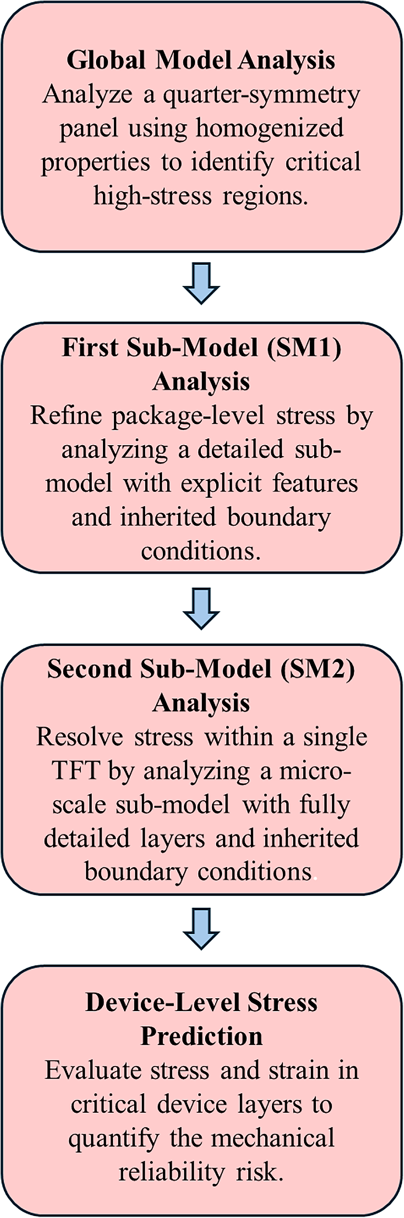
Global and sub-model technique
A full-scale finite-element model that explicitly resolves every micro-scale feature, such as individual solder bumps and TFT device structures, would be computationally prohibitive. To overcome this challenge, a multi-scale sub-modeling methodology was employed. The complete hierarchical workflow, illustrating the idealization of the physical structure for the finite-element analysis, is shown in Figure 5. This multi-stage analysis procedure is schematically summarized in Figure 6, showing the conceptual transition from a global panel-level model to a localized sub-model and finally to a detailed sub-sub-model of the individual TFT cell. The approach began with a coarse global model to identify critical stress regions, followed by successive, refined local sub-models to analyze these regions with progressively higher fidelity. This study utilized a two-level hierarchical approach: a first-level sub-model (SM1) and a second-level sub-model (SM2).

The analysis procedure for the global and sub-models of the TFT-FOPLP. TFT-FOPLP: thin-film transistor fan-out panel-level packaging.
Schematic diagram of the hierarchical sub-modeling approach.
The primary rationale for SM1 was to bridge the vast difference in scale between the simplified global model and the detailed structure of a single-package module. The global analysis identified the die corner near the panel edge as a high-stress region, but its homogenized layers could not resolve local stress concentrations. Therefore, SM1 was constructed to achieve a higher fidelity analysis of this critical area. The idealization for SM1 involved a significant increase in detail: features that were homogenized in the global model, such as the silicon die, individual solder bumps, and underfill, were now explicitly modeled with their actual geometries (Figure 7(b)). For the finite element method (FEM) model, the cut boundaries of SM1 inherited their boundary conditions from the parent model through an interpolation of the nodal displacement field. A refined mesh, finer than that of the global model, was used to accurately capture the stress gradients around these newly detailed geometric features.

Hierarchical sub-modeling approach from global panel to a single TFT cell: (a) global model identifying the critical region, (b) SM1 of the die corner, and (c) SM2 resolving the TFT cell geometry. TFT: thin-film transistor; SM1: first-level sub-model; SM2: second-level sub-model.
The rationale for SM2 was to achieve the final, device-level resolution required to assess the reliability of a single TFT cell. The SM1 analysis confirmed the peak stress location to be in the TFT layer directly above a specific die corner solder bump. SM2 was therefore defined as a small block (approximately 400 μm × 400 μm) centered on this location to resolve how this aggregate stress was distributed among the fragile micro-layers of the transistor. The idealization involved replacing the homogenized TFT layer with a fully detailed micro-architecture of the TFT cell, explicitly modeling the M1, M2, and M3 metal layers, the poly-Si channel, and all constituent dielectric layers (Figure 7(c)). For the FEM model, displacement boundary conditions for SM2 were similarly derived by interpolating the displacement field from its parent model, SM1. To accurately capture steep stress gradients, a very fine mesh with a minimum element size of about 2 μm was employed in the critical channel region. This hierarchical technique effectively transfers the deformation behavior from the global panel scale down to the micro-scale of an individual device without prohibitive computational cost.
The material properties for the explicitly modeled features in the sub-models were taken from Tables 1 and 3. The decision to use a linear elastic model for all materials was a deliberate choice based on the study's primary objectives. While many polymer materials in the structure exhibit viscoelastic (time-dependent) behavior, a linear elastic assumption is a standard and appropriate simplification for this type of analysis. The main goal was to identify the locations of maximum stress concentration and provide a first-order, conservative estimate of the peak stresses induced by CTE mismatch after the fabrication cool-down. The analysis focused on the final, stabilized stress state, for which an elastic model provides a reliable upper-bound estimation and critical design insights without the prohibitive computational cost and extensive material characterization required for a full viscoelastic simulation.
Results
The thermo-mechanical simulation results are presented in this section, following the hierarchical, global-to-local modeling approach. The findings from the global panel-level model are presented first, focusing on the overall package deformation and the identification of critical high-stress regions. Subsequently, the results from the first-level sub-model are detailed, which provide a more refined stress analysis of the identified critical location. Finally, the detailed stress and strain distributions within the micro-scale structures of a single TFT cell, as predicted by the second-level sub-model, are presented and their implications discussed.
Global model results
The global panel-level simulation yielded predictions of the overall package warpage and identified critical regions of high stress concentration. The analysis indicated that significant panel warpage occurs upon cooling from fabrication temperatures. This phenomenon is primarily attributed to the large CTE mismatch between the rigid glass substrate and the various polymer and metallic layers it constrains during thermal contraction. The magnitude of this warpage was predicted to be most pronounced at the panel's free edges and corners.
A key finding from the global model was the precise location of the maximum principal stress within the homogenized TFT layer. The peak stress was consistently observed in the outermost package modules, specifically at the corner of a die situated near the panel's periphery, as illustrated by the region selected for the sub-model in Figure 6(b). This localization is a direct consequence of the greater mechanical constraints and differential thermal contraction experienced in this area.
Physically, this location represents a confluence of materials with highly dissimilar CTEs—notably the silicon die, solder bumps, and the surrounding polymer underfill. This convergence of materials induces a complex, triaxial stress state in the overlying TFT structures. The global analysis therefore successfully established this die corner as a significant stress concentration point, motivating its selection for the detailed sub-model analysis discussed next.
First sub-model results
The analysis of the SM1, which provided a detailed representation of a single-package module, yielded a more refined prediction of the local stress state. The results confirmed that the maximum principal stress within the homogenized TFT layer is concentrated at the corner directly above the die's corner solder bump, a finding that corroborates the prediction from the global model. The peak stress value in this region was calculated by SM1 to be approximately 50 MPa.
As anticipated, this magnitude is higher than the value estimated by the coarser global model. The increase is attributed to the higher fidelity of SM1, which incorporates a refined mesh and explicit geometric features (e.g. individual solder bumps) that better resolve the local stress concentration. The primary output of this analysis stage was the extraction of the displacement field from the region surrounding this peak stress location. These displacements serve as the driving boundary conditions for the final, SM2. It is important to note that the stress value from SM1 represents an average across the entire homogenized TFT layer. The subsequent SM2 analysis, therefore, aims to resolve how this aggregate stress is distributed among the individual, fragile micro-layers of an actual TFT cell.
Second sub-model (TFT cell) results
The SM2 enabled a high-fidelity analysis of the stress distribution within the detailed micro-architecture of a single TFT cell, explicitly resolving its individual constituent layers. The results for the brittle dielectric and semiconductor components are summarized in Table 4. The analysis revealed that the GI is subjected to a significant tensile stress of approximately 44.5 MPa, localized at the edges of the conductive channel. A corresponding principal strain in the poly-Si of about 0.1% was also observed. While the channel region is functionally critical, the highest stress among all brittle layers, at approximately 407 MPa, was predicted in the top passivation layer PV, highlighting the dielectric stack as a primary concern for mechanical fracture. In parallel, the ductile metallic layers were evaluated using the von Mises stress criterion (Table 5). The highest von Mises stress, found in the uppermost metal layer (M3), was about 415 MPa. Although these stress levels are below the typical yield strength of copper, suggesting plastic deformation is unlikely, their magnitude is substantial and could pose a risk to long-term reliability through mechanisms such as fatigue.
Predicted maximum principal stress in the brittle materials of the TFT cell.

TFT: thin-film transistor.
Predicted maximum von Mises stress in ductile materials of the TFT cell.

TFT: thin-film transistor.
These simulation results identify the GI and adjacent dielectric layers as the most mechanically vulnerable components within the TFT structure. Within the critical channel region, the predicted maximum principal stress in the GI corresponds to a tensile strain of about 0.1%. Although this strain level is below the typical fracture strength of the dielectric material, and thus unlikely to cause immediate mechanical failure, it is significant enough to induce measurable shifts in the TFT's electrical characteristics, such as its threshold voltage. The underlying physical mechanism involves the modulation of the energy band structure in poly-Si and the generation of trap states at the semiconductor–dielectric interface, leading to behavior analogous to bias stress instability. While a full electrical characterization was outside the scope of this mechanical investigation, the predicted tensile strain concentration at the channel edges is expected to result in performance degradation, such as an increase in threshold voltage or a decrease in carrier mobility for an n-channel TFT.
Therefore, the methodology developed in this study—which links package-level, process-induced stress to micro-scale device deformation—establishes the groundwork for a predictive model of electrical parameter drift in packaged TFTs. Future work could extend this framework by integrating these simulation results with experimental data on the electrical response of TFTs under controlled mechanical strain, thereby enabling the development of fully physics-based reliability models that correlate stress to specific electrical failure criteria.
Discussion
The simulation results presented herein elucidate the complex thermo-mechanical behavior of the TFT-FOPLP structure, offering critical insights at both the package and device levels. At the package level, the analysis confirms established principles in electronic packaging: the large-area panel is susceptible to significant warpage and stress gradients, particularly near its free edges and corners. This finding substantiates the design choice of an unpopulated border as a prudent reliability strategy. Similarly, the localization of maximum stress at the corners of the silicon dies is a well-understood phenomenon, driven by the convergence of materials with highly dissimilar CTEs (e.g. copper at ∼18 ppm/°C vs. glass at ∼3.8 ppm/°C). Our work corroborates these foundational principles and, critically, quantifies their effects for the specific, complex architecture of a TFT-FOPLP, particularly in the regions beneath the silicon dies (CTE ∼2.8 ppm/°C) where high-CTE solder bumps (∼21 ppm/°C) create a localized, complex stress state.
The primary novelty of this investigation lies at the device level, where the analysis highlights the GI of the TFT cell as a mechanically critical location. While the predicted maximum principal stress in the GI (approximately 44.5 MPa) is below the nominal fracture strength of SiO2, it represents a non-trivial stress level that could, over time, contribute to long-term degradation mechanisms like stress-corrosion cracking, especially if pre-existing nanoscale flaws are present. For the poly-Si active layer, the primary concern is not immediate mechanical fracture but rather the impact of strain on electrical performance. Building upon prior studies that have established the strain sensitivity of poly-Si devices, our work provides a key contribution by quantitatively predicting the specific strain level (approximately 0.1%) that results directly from the panel-level manufacturing process. As prior studies have established, even strains of this order can alter grain boundary trap densities and carrier mobilities in poly-Si, leading to measurable shifts in device characteristics like threshold voltage. This underscores the necessity of ensuring that package-induced strain remains within the operational tolerance limits of the embedded circuitry.
The multi-scale modeling approach demonstrated in this work proved essential for resolving these localized device-level stresses. It is this integrated framework—which creates a direct, quantitative link from a macro-scale cause (panel fabrication) to a micro-scale consequence (strain in a single transistor)—that constitutes the core contribution of this study. While the individual modeling techniques are established, their application to bridge this analytical gap for an active TFT-FOPLP system is novel.
It is important to acknowledge a key assumption in this study: the perfect adhesion between all material interfaces. While this idealization is necessary for a tractable model, the high interfacial stresses predicted by the simulation—particularly at the die corner regions where multiple material interfaces converge—suggest that delamination could be a potential failure mode in a physical device. This highlights the practical importance of robust adhesion and suggests that geometric features, such as underfill fillets, could be crucial for mitigating stress concentrations at these interfaces.
Ultimately, this investigation affirms that the TFT-FOPLP concept is mechanically feasible, provided that careful design attention is paid to mitigating stress in the most vulnerable regions. The presented methodology provides a valuable tool for design-for-reliability. This information can inform design rules, such as restricting the placement of critical TFT circuitry in known high-stress zones (e.g. near die corners) or strategically reinforcing these areas. This predictive capability allows for the proactive management of thermo-mechanical challenges inherent in this promising technology
Conclusion
This study successfully developed and applied a comprehensive, multi-scale thermo-mechanical simulation framework to evaluate the reliability of a large-format TFT-FOPLP. The primary contribution of this work is the establishment of a predictive methodology intended for design-for-reliability, enabling the identification of potential high-stress regions and failure modes early in the development cycle, prior to physical prototyping. The major outcomes of this numerical investigation are summarized as follows:
Development of a hierarchical modeling framework: A multi-scale, global-to-local sub-modeling methodology was implemented. The primary contribution of this work is the application and integration of these techniques to create an effective and computationally efficient tool for predicting process-induced stress distribution from the overall panel deformation down to the individual layers of a micro-scale transistor in a TFT-FOPLP system. Identification and quantification of critical high-stress regions: The simulation results confirmed the expected primary regions of stress concentration at the panel's periphery, specifically at the corners of the silicon dies, which is consistent with established mechanical principles in advanced packaging. This finding is critical for informing design-for-reliability rules, such as the strategic placement of sensitive circuitry. Quantitative prediction of stress in the TFT channel: At the device level, the analysis provided key quantitative predictions for the most critical components. The GI layer is subjected to a peak principal tensile stress of approximately 44.5 MPa, with the poly-Si channel experiencing a corresponding tensile strain of about 0.1%. While this stress is likely below the material's fracture strength, the predicted strain level provides a quantitative basis for future work to correlate manufacturing processes with potential shifts in the device's electrical parameters. Comprehensive reliability risk assessment: The analysis also quantified risks in other layers. Brittle dielectric layers, such as the top passivation layer, were predicted to experience significantly higher stresses (approximately 407 MPa), indicating a primary risk of mechanical fracture. In contrast, the ductile metallic interconnects experienced maximum von Mises stresses of up to 415 MPa, which is below the typical yield strength but could pose a risk to long-term reliability.
It is important to emphasize that this study is a foundational, numerical investigation, and we acknowledge that the quantitative accuracy of the model's predictions has not yet been validated through direct experimental comparison. To build upon the foundational framework established here, future work should focus on a comprehensive experimental validation campaign. This would involve correlating the model's predictions with physical measurements, such as measuring global panel warpage with optical methods like digital image correlation and assessing local strain in critical regions. By completing this essential next step, the predictive model can be refined, thereby establishing robust, quantitative design rules that link manufacturing processes to the long-term reliability of this promising technology.
Footnotes
Acknowledgement
The authors also acknowledge the support of the National Center for High-Performance Computing (NCHC) for providing the computational resources and facilities used in this work.
Ethical considerations and consent statement
Ethical approval was not required for this study as it is based entirely on computational modeling and simulation. The research did not involve human participants, animal subjects, or any personal data.
Author contributions
Hsien-Chie Cheng: conceptualization, supervision, project administration, funding acquisition, and writing—review and editing. Ching-Feng Yu: conceptualization, methodology, software, validation, formal analysis, investigation, and writing—original draft.
Funding
The authors disclosed receipt of the following financial support for the research, authorship, and/or publication of this article: This research was partially funded by the National Science and Technology Council (NSTC) of Taiwan, ROC, under grant numbers NSTC 113-2221-E-035-031-MY3 and NSTC 114-2222-E-239-003.
Declaration of conflicting interests
The authors declared no potential conflicts of interest with respect to the research, authorship, and/or publication of this article.
Data availability statement
The data that support the findings of this study are available from the corresponding author upon reasonable request.