
Abstract
Aiming at the problem of bus voltage control in DC microgrid, a dynamic compensation control strategy based on a residual generator is designed to complete the voltage compensation of DC-DC converter. Firstly, based on the DC microgrid system architecture, the bus voltage fluctuations are analyzed theoretically, and then the DC-DC converter state-space mathematical models of the DC microgrid system are established to obtain the input-output relationship of the control system. Based on the theory of double coprime decomposition and Youla parameterization stable controller, the proposed control architecture based on the residual generator is obtained, and the output value generated by the current disturbance is compensated in reverse by applying model matching theory. The voltage loop compensation controller Q(s) is obtained by the linear matrix inequality method (LMI), and the current loop compensation controller H(s) is designed according to the dynamic structure diagram of the DC-DC converter. Hardware-in-the-loop simulation (HILS) results show that the architecture can improve the dynamic performance of the DC-DC converter without changing the original system structure parameters, and suppress the DC bus voltage fluctuations caused by load switching, power fluctuations, and AC-side load imbalances, and enhance the robustness of the system.
Keywords
Introduction
The DC microgrids integrate distributed generations (DGs) efficiently and flexibly in the form of DC, with simple structure and high reliability. 1 There are several advantages of DC microgrids: (1) most energy storage systems have natural DC characteristics, 2 (2) compared to AC microgrids, DC microgrids reduce the number of converter, 3 (3) DC microgrids do not need to consider frequency and reactive power, and have higher power quality and efficiency,4,5 (4) avoid circulating currents caused by frequency and phase inconsistency, (5) DC bus voltage is the key indicator to evaluate the stability of DC microgrid. 6
The main reason for DC bus voltage fluctuations is the change in active power. The main reasons for active power changes are load switching and distributed power generation fluctuations. 7 Furthermore, when the three-phase AC load is unbalanced, the DC bus voltage exhibits a voltage fluctuation of double-frequency. 8
The conventional PI dual-loop control strategy is usually adopted. However, the traditional control strategy cannot improve the response speed of the system under the premise of suppressing the DC bus voltage fluctuation. Recently, several methods have been proposed to reduce the fluctuation of the DC bus voltage. These methods can be classified as passive methods by access external devices and active methods of improving the controller. 9 In Bhosale and Agarwal, 10 a hybrid energy storage control scheme based on fuzzy logic is proposed, this method can mitigate the transients in the dc bus voltage due to the fast-changing power conditions in the load. The proposal of incorporating electric springs to reduce the impact of intermittent renewable energy on the DC bus voltage is reported in Yang et al. 11 and Wang et al. 12 In Cao et al., 13 a ripple eliminator is adopted to reduce the ripple of the DC bus voltage, which is a bidirectional buck-boost converter terminated with an auxiliary capacitor. However, the above method needs to be based on additional equipment, which increases the complexity and cost of the system. Therefore, many scholars have optimized and improved the traditional dual-loop control structure. To improve the control performance of the bus voltage, the external disturbance current or power is introduced as a feedforward amount into the double closed-loop structure, and the disturbance current or power is directly tracked to reduce the bus voltage fluctuation.14,15 In Liu et al. 16 and Lu et al. 17 a control method based on the extended state observer is proposed, which has strong robustness. Furthermore, an observer-based current feedforward compensation method is proposed in the literature 7 and, 18 with the proposed control scheme, the dynamic response of dc voltage control can be improved effectively through using an observer. However, all of the above methods need to change the structure of the original dual-loop controller.
The main contributions of this work are summarized as follows:
A dynamic compensation control structure based on a residual generator is put forward for the DC microgrid system. The method can compensate for the control signal without changing the structure of the original double closed-loop controller.
The different forms of current disturbances as interference inputs to obtain the residual signal. Through controlling voltage compensation, the system maintains good performance and acquires the robustness of the DC microgrid under interferences.
The voltage loop compensation controller is designed by the linear matrix inequality method (LMI). Besides, the current loop compensation controller is introduced to suppress the secondary disturbance caused by the voltage loop compensation signal.
The treatment of existing devices initiatively and multi-functionally and the development of advanced technical support for power quality management.
This paper is organized as follows. In section II, the analysis of DC bus fluctuations is presented. The model of the Buck converter and Boost converter is introduced in section III. Section IV is devoted to the proposed dynamic compensation control structure and the solution method of the compensation controllers. Then in section V, HILS results show that the strategy significantly improves the anti-interference ability of the DC bus voltage. Finally, the conclusions are given in section VI.
Analysis of DC bus fluctuations
DC microgrid system structure
The typical architecture of DC microgrids is shown in Figure 1. The power generation units include wind turbines and photovoltaics. The loads include DC loads and AC loads. The DC loads can be directly connected to the DC bus or through DC-DC converters. The AC loads are connected to the DC bus through the DC-AC converters. In the grid-connected mode, the DC microgrid can realize energy interaction with the AC microgrid via a bidirectional DC-AC converter. In island mode, the energy storage systems are controlled to achieve the energy balance of the DC microgrid and keep the DC bus voltage stable.
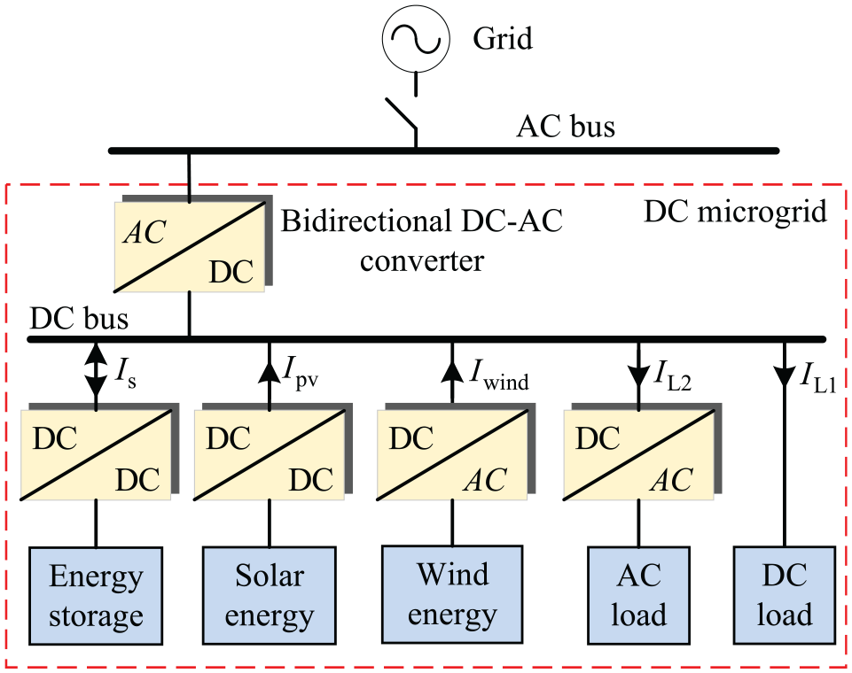
Typical architecture of DC microgrid.
Analysis of DC bus voltage fluctuation
The voltage equation of a bus capacitor in Figure 1 can be written as:

where Cdc and Vdc are the DC bus capacitance and voltage, respectively, Is is the output current of the energy storage system, Ipv and Iwind are the output currents of the photovoltaic and wind turbines, respectively, and IL1 and IL2 are the currents of the DC load and the AC load, respectively.
It can be known from (1) that the stability of Vbus is closely related to the current changes caused by distributed generations and loads connected to the DC bus. According to the mechanism of DC bus voltage fluctuation, it can be divided into transient fluctuation and steady-state fluctuation. Transient problems refer to the temporary rise and fall of DC bus voltage caused by loads or DGs switching. Steady-state problems include persistent disturbances caused by long-term random changes in power such as DGs and loads. Besides, when the AC load is unbalanced in three phases, a negative sequence component is generated, which causes the DC bus voltage to fluctuate continuously. According to the symmetric component method 19 :

where idc is the the DC bus current, UNm is the AC rated voltage amplitude, Uc is the carrier voltage amplitude of the DC-AC converter, ω is the angular frequency, Ip and φ1 represent the amplitude and phase of the positive sequence component of the current, In and φ2 represent the amplitude and phase of the negative sequence component of the current, respectively.
If the three-phase load is balanced, the negative sequence component is zero; if the three-phase load is unbalanced, the negative sequence component causes the double-frequency fluctuation of the DC bus voltage.
Mathematical model of DC-DC converter in DC microgrid
The DC microgrid consists of different DC-DC converters in parallel. Different DC-DC converters are applied according to user needs. Typical DC-DC converters include buck converters and boost converters, as shown in Figure 2.

Typical DC-DC converter: (a) buck converter and (b) boost converter.
Mathematical model of buck converter
According to Figure 2(a) and Kirchhoff’s law, the differential equation expression of the buck converter can be obtained:

where Rt,i, Lt,i, Ct,i are the parasitic resistance, inductance and capacitance of the i-th converter, respectively; Vt,i and Vi are the instantaneous voltage and output voltage of the switching transistor of the i-th converter, respectively; It,i and Io,i are the inductor current and output current of the i-th converter, respectively.
The input signal of the DC-DC converter is the duty cycle, and the output voltage can be controlled by controlling the duty cycle. The amplitude vc,i and period of the carrier are generally fixed, so the input signal of the mathematical model of the controlled object can be converted into a modulated wave.
According to the PWM modulation principle, the average value of Vt,i can be obtained:

where uk,i are the modulation wave of the i-th converter; Ui and
Replace the original input Vt,i with

where

Mathematical model of boost converter
Similarly, the differential equation of the boost converter can be obtained:

where dj is the duty cycle.
The boost converter is different from the buck converter and contains two non-linear terms (1−dj)Vj and (1−dj)Vj, so it needs to be linearized. Define V0,j, It0,j, Io0,j, d0,j as the steady-state operating points of the boost converter, and obtain its linearized state-space expression:
where:

Similarly, the input of the boost converter can also be converted into a modulated wave. When the maximum value of the carrier is 1 and the minimum value is 0, the input is d0,j−dj.
Dynamic compensation control architecture based on residual generator
Control architecture based on residual generator
Assume that

and let
where


where
Based on the Youla parameterization, all controllers that internally stabilize the control loop can be parameterized by

where
When the original closed-loop system is stable, adding a compensation controller

where
The expression of the luenberger observer is:

where
The
where
From the above theory, the control architecture based on the residual generator shown in Figure 3 can be obtained.

The control architecture based on the residual generator.
Solution of voltage loop compensation controller
According to the superposition theorem, when

where
The control goal of this paper is to find a suitable compensation controller
State-space expressions can be transformed into transfer function expressions by

It is assumed that the observer gain matrix

where ZLC,i = Lt,iCt,i, ZRC,i = Rt,iCt,i.

The model matching structure of the buck converter.
According to the model matching theory, if there exisits Qp,i so that zp,i = 0, a perfect disturbance compensation can be achieved. The expression of Qp,i can be obtained:

The numerator order of the Qp,i expression obtained by (19) is higher than the denominator order. Therefore, an approximate transfer function expression of Qp,i is obtained by adding a compensation term such that the denominator order is greater than or equal to the numerator order. The simplest form of Qp,i is a second-order system:

where η is a small constant.
The above-mentioned solving method has its limitations and can only be used for solving the minimum phase system. The boost converter is a typical non-minimum phase system with a positive zero point in its transfer function. 23 The controller Qp,i obtained by using (19) contains a positive point, that is, the obtained controller is unstable. Model matching theory can be transformed into the form of generalized control objects. Therefore, this paper applies LMI to solve the controller Qp,i when the converter is a typical non-minimum phase system. It is worth mentioning that LMI is suitable for both minimum-phase systems and non-minimum phase systems. According to the Figure 4, the generalized control structure can be show as Figure 5.

The generalized control structure.
The state-space expression of the generalized control object is:

where Dg11,i, Dg12,i, Dg21,i, and Dg22,i are

Let the state-space equation of the controller Qp,i be:

Since the generalized control object is controllable and observable, and

the system matrices in (24) are given as follows:

The system is asymptotically stable, and ||G(s)||∞ < μ.
There is a symmetric positive definite matrix
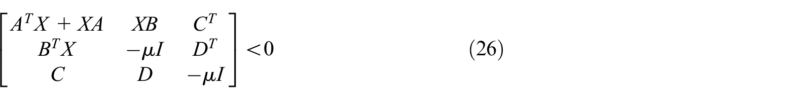
According to Theorem 1, Qp,i satisfies:

The matrix variable

where

The solution of Qp,i can be obtained by solving matrix inequality (28).
Design of current loop compensation controller
If the buck converter adopts single-voltage closed-loop control, the dynamic compensation of voltage can be achieved by adding only Qp,i. If the buck converter uses voltage and current double closed-loop control, the secondary disturbance caused by Qp,i need to be considered. This paper eliminates the effects of secondary disturbances by designing a current loop compensation controller. According to Kirchhoff’s law and Laplace transform:

Apply control architecture based on the residual generator to the buck converter gives the equivalent structure shown in Figure 6, which illustrates the principle of current loop compensation.
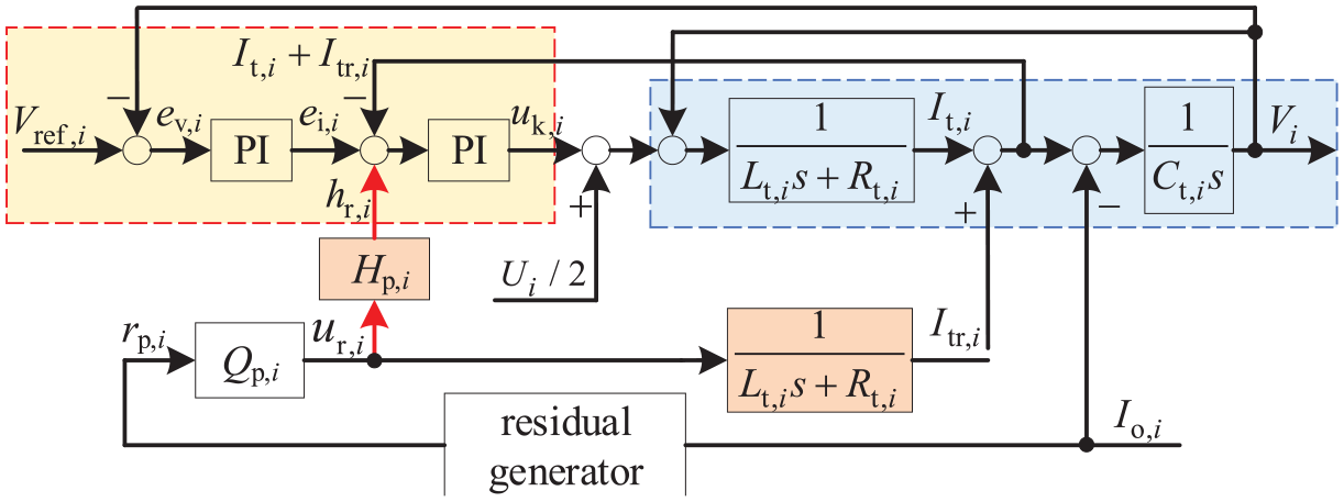
Schematic diagram of current loop compensation.
As can be seen from Figure 6, when the system is stable, ev,i = 0 and ei,i = 0. When a disturbance occurs, the voltage loop compensation controller Qp,i is superimposed on the output of the controller, so that the sum of the increase of the inductor current Itr,i and the disturbance current Io,i is 0, thereby keeping the converter output voltage Vi constant. At this time, ev,i = 0. However, the inductor current is also the amount of feedback. Although the inductor current increment Itr,i cancels the disturbance current, the change in ei,i causes the original control output to change. In order to keep the original controller output unchanged, it is only necessary to make the sum of the inductor current increase caused by Qp,i and the output of the current loop compensation controller Hp,i equal to 0, that is,

where Hp,i is the required current loop compensation controller.
Therefore, the current loop compensation controller is:

Complete proposed control structure
The complete dynamic compensation control architecture of the buck converter is as follows:
In Figure 7, when there is no disturbance current, the residual rp,i = 0. At this time, the output ur,i of the voltage loop compensation controller Qp,i is zero, and the output hr,i of the current loop compensation controller Hp,i is zero, this structure is completely equivalent to double closed-loop control. When the disturbance current occurs, the residual generator immediately outputs the residual signal. The control signal ur,i generated by Qp,i directly acts on the double closed-loop control output. Hp,i acts on the input end of the current inner loop, canceling the secondary disturbance brought by Qp,i, and making the original controller output not changing.

The complete dynamic compensation control architecture of the buck converter.
Hardware-in-the-loop simulation
In order to verify the dynamic compensation effect of the proposed method, experiments were performed based on the AppSIM hardware-in-the-loop simulation platform. Figure 8 shows the HILS environment, which composed of the target simulator, host computer, DSP (TMS320F28335), interface box, connection board, and oscilloscope. The DC microgrid in Figure 1 has been implemented by the MATLAB/Simulink software, and the code is generated by AppSIM software and downloaded to the target simulator. The control algorithm is imported into the DSP controller through CCS software and provides control signals through the connection board. This paper applies master-slave control, the converter of the energy storage system uses the proposed control architecture, other converters use current control, and inverter uses V/f control. The parameters of each converter are shown in Table 1.

AppSIM HILS platform.
Parameters of each converter.

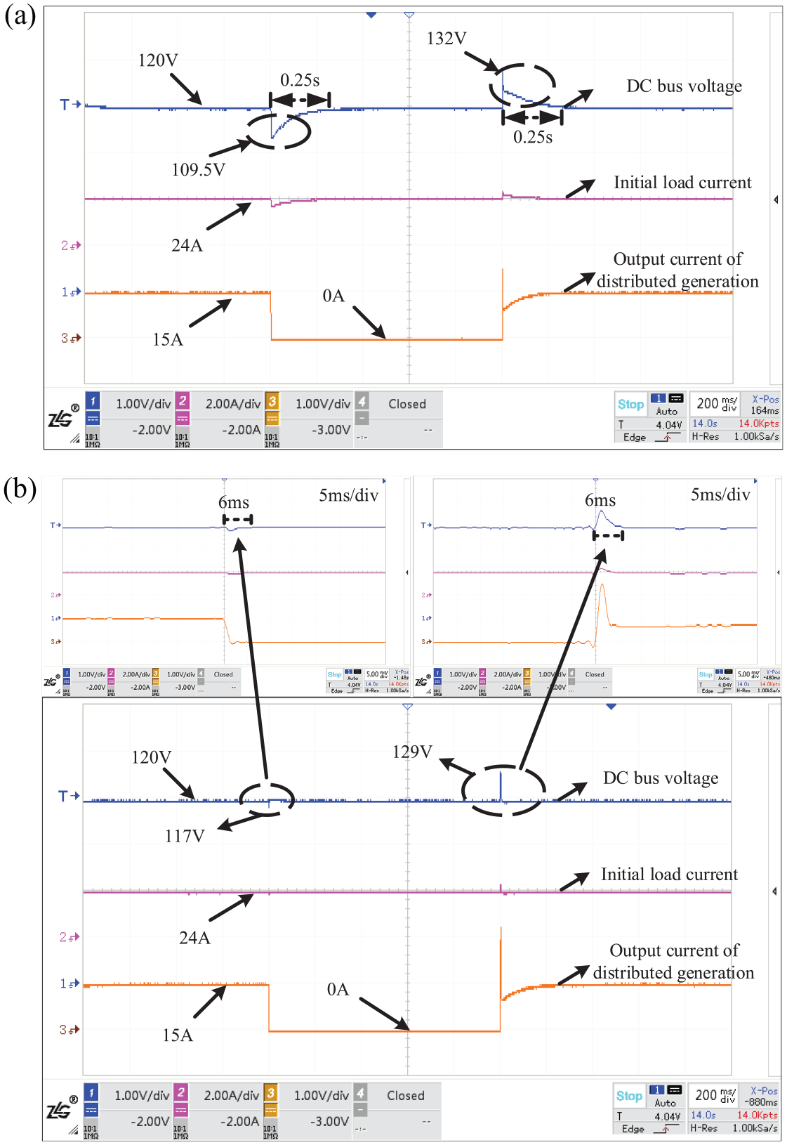
Case 1: Load switching experiment
The first case evaluates the anti-interference ability of the DC bus voltage under load switching conditions. The steady-state value of the DC bus voltage is 120 V. The load resistance drops from 10 Ω to 5 Ω at t0. The load resistance increases from 5 Ω to 10 Ω at t1. Figure 9 shows the waveform comparison between the double closed-loop control and the proposed control strategy under load switching conditions. It can be seen from Figure 9(a) that under the double closed-loop control strategy, when the load resistance suddenly decreases, the DC bus voltage will drop about 15 V and returns to 120 V about 0.23 s; Similarly, when the load resistance suddenly increases, the DC bus voltage will overshoot about 16 V and returns to 120 V about 0.23 s. It can be seen from Figure 9(b) that under the same experimental conditions, the proposed control strategy can effectively reduce the fluctuation of the bus voltage and significantly improve the dynamic response speed of the bus voltage.

The experimental results of load switching: (a) double closed-loop control and (b) the proposed control strategy.
Case 2: Distributed generation switching experiment
In the second case study, we evaluate the plug-and-play capabilities of DGs under the proposed control strategy. To this end, it is assumed that photovoltaic is plugged out from the DC microgrid in Figure 10 at t0 and it is plugged in at t1. Due to this PnP operation, the DC bus voltage is affected. It can be known from Figure 10 that under the double closed-loop control strategy when the distributed power generation is plugged out, the bus voltage drops about 11 V and returns to 120 V about 0.25 s; similarly, when the distributed generation is plugged in, the DC bus voltage increases about 12 V and returns to 120 V about 0.25 s. Under the same experimental conditions, the proposed control strategy significantly improves the anti-interference ability and dynamic response speed of the DC bus voltage and is conducive to the realization of plug and play.
The experimental results of distributed generation switching: (a) double closed-loop control and (b) the proposed control strategy.
Case 3: Experiment on output power fluctuation of distributed generation
Case 3 evaluates the performance of the proposed control strategy in distributed generation output power uncertainly. In order to facilitate analysis, we use a sinusoidal current disturbance with a period of 1 s and an amplitude of 5 A to simulate the output power fluctuation of distributed generation. Figure 11 shows the performance of the proposed control strategy. Through experimental comparison, it can be seen that under the double closed-loop control strategy, the DC bus voltage is affected by distributed generation and shows a sinusoidal fluctuation, and load current also shows sinusoidal fluctuations following voltage; While the proposed control strategy can effectively suppress the bus voltage fluctuations caused by the output power fluctuations of distributed generation and keep the bus voltage constant.

The experimental results of output power fluctuation of distributed generation: (a) double closed-loop control and (b) the proposed control strategy.
Case 4: AC load imbalance experiment
AC loads can get power from the DC bus through the converter. However, when the three-phase AC load is unbalanced, the DC-side current of the AC load will be superimposed with a current component of 2f Hz (100 Hz). The proposed control method is applied to the converter of the energy storage system and compared with the traditional voltage control method as shown in Figure 4.
We consider adding an unbalanced AC load at t0. It can be known from Figure 12 that when the AC load is unbalanced, the DC bus voltage has a sinusoidal fluctuation with a period of 0.01 s and an amplitude of 6 V. Under the same experimental conditions, when the proposed control strategy is adopted, the fluctuation amplitude of the DC bus voltage is significantly reduced. Therefore, the proposed control strategy can reduce the impact of AC unbalanced load on the DC bus voltage.

The experimental results of AC load imbalance: (a) double closed-loop control and (b) the proposed control strategy.
Conclusion
This paper aims at the DC-DC converter in micro-grid in island mode and improves it based on the voltage and current double closed-loop control. A dynamic compensation control strategy based on a residual generator is proposed. The control strategy has a simple structure and is easy to implement. It improves the robustness of the system without affecting the performance of the original double closed-loop control system. The hardware-in-the-loop simulation results show that the proposed control strategy can effectively suppress the transient impact caused by load and distributed generation switching. At the same time, it can suppress the DC bus voltage fluctuation caused by random power fluctuation, and reduce the impact of the three-phase load imbalance on the AC side on the DC bus voltage. This control strategy significantly improves the anti-interference ability and dynamic response speed of the DC bus voltage, which is conducive to the realization of the plug and play function.
Footnotes
Declaration of conflicting interests
The author(s) declared no potential conflicts of interest with respect to the research, authorship, and/or publication of this article.
Funding
The author(s) disclosed receipt of the following financial support for the research, authorship, and/or publication of this article: This work was supported in part by the National Key R&D Program of China under Grant 2018YFC0809700, in part by the National Key R&D Program of China under Grant 2021YFE0103800, in part by the National Natural Science Foundation of China under Grant 51777002, and in part by the Beijing High Level Innovation Team Construction Plan under Grant IDHT20180502.