
Abstract
In this paper, low-noise incremental delta–sigma analog front end (AFE) integrated circuit (IC) for capacitive microsensors is presented. A conventional capacitance-to-digital converter (CDC) mainly uses a multi-stage capacitive sensing amplified stage (CSA) and analog-to-digital converters. The multi-stage CSA is not suitable for application in various Internet of things (IoT) devices that require low power because the power consumption of the analog front-end circuit increases in proportion to the number of amplifiers and the chip area increases. So, the presented delta-sigma AFE can convert the capacitance changes to the digital codes directly. This structure can achieve a small active area and low power consumption. The delta–sigma AFE achieves low-noise and high linearity using a capacitor polarity swapping technique. The measured effective resolution is 16.2 bits, and the non-linearity is 0.05% full-scale output (FSO). The integrated circuit is implemented in a 0.18-µm standard CMOS process. All functional blocks, including the analog circuits (bandgap reference, voltage reference, and delta–sigma capacitance-to-digital converter) and digital block (accumulator and timing generator), are integrated on a chip. The proposed incremental delta–sigma AFE consumes 1.12 mW of power from a 3.3-V supply at a sampling frequency of 500 kHz and occupies a total active area of 0.42 mm2.
Keywords
Introduction
Over the past years, capacitive micro-electro-mechanical-systems (MEMS) sensors have been applied to a variety of devices, especially along with the advent of the Internet of things (IoT). The MEMS sensors used in smart devices such as smart phones, tablet PCs, wearable devices, and so on, require smaller size, longer battery life, and higher signal quality. The sensor interfaces with low-power, low-noise, high resolution, and high accuracy in a small area are highly desirable. 1–3
The capacitive sensing schemes are widely used in many sensor applications, and the various readout integrated circuits (ICs), including the capacitive analog front end (AFE) and capacitance-to-digital converter (CDC) like successive approximation register (SAR) CDC, high-order switch-capacitor (SC) delta–sigma CDC, and have been presented. 2–7
In conventional CDC, the two-step conversion schemes including capacitance to voltage conversion and voltage to digital conversion are generally used. Recent researches on capacitive readout IC favor direct conversion of capacitance to a digital code for higher accuracy and lower power consumption. A low-power CDC based on a SAR algorithm without a pre-amplifier, one of the direct conversion schemes, has been proposed. 8 The SAR CDC without a pre-amplifier can achieve low-power consumption but is sensitive to parasitic components because the sensing capacitance is connected to a high-impedance input. 7 Recently, a high-order SC delta–sigma CDC with various schemes has been proposed to achieve high resolution. 9
Delta–sigma modulation is an efficient method for obtaining high resolution in low-frequency applications such as sensor interfaces, and is preferred for high-resolution CDC.
A chopper stabilization is widely used in combination with the delta-sigma CDC for reducing low frequency noise, however the residual offsets due to the process variation and non-ideal switching operation are disadvantages. 10 The capacitor polarity swapping with the demodulation chopper in the feedback path can reduce the residual offsets, and can suppress the gain and sensitivity errors due to the parasitic capacitances. 11
Figure 1 shows the architecture of the proposed low-noise incremental delta–sigma AFE with capacitor polarity swapping technique for capacitive microsensors. The proposed AFE consists of voltage reference, current reference, 12C interface, timing generator, first order delta-sigma modulator and 16-bit accumulator. Architecture of the proposed low-noise incremental delta–sigma analog front end with capacitor polarity swapping technique for capacitive microsensors.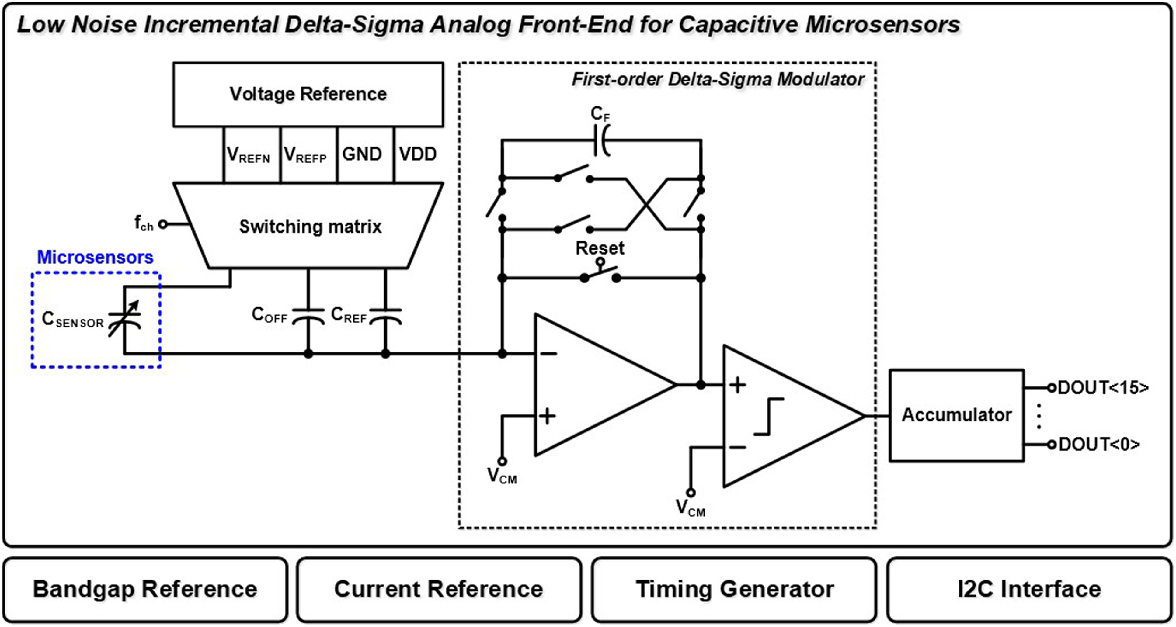
Proposed AFE adopted the capacitor polarity swapping. It can reduce the leakage current by the SC operation of the input chopper and can reduce the input current noise, thus, higher accuracy can be achieved. SC operation control the state of the switch connected to two phase by switching matrix. Two phase (P1, P2) are change COFF and CREF value can make reduce offset and leakage current and transfer CSENSOR signal to delta-Sigma integrator. The detail of SC operation is described in Proposed Delta-Sigma CDC.
This paper presents a low-noise incremental delta-sigma AFE with capacitor polarity swapping for capacitive microsensors. High accuracy, small area, and wide capacitance range are achieved using a first-order delta–sigma modulator. The input capacitance range can be programmable by adjusting the reference voltages. The input capacitance can be controlled from 4 pF to 32 pF when the reference voltage is changed from 0 V to 1 V.
A simple accumulator logic based on 16-bit up-counter is used for converting the bitstream output of the delta-sigma modulator to the 16-bit digital code.
This paper is organized as follows. Proposed Delta-Sigma CDC presents the proposed incremental delta–sigma AFE. Experimental Results describes the measurement setup and results. Finally, Conclusions briefly concludes this work.
Proposed Delta-Sigma CDC
A typical first-order delta–sigma CDC with conventional chopper stabilization technique is shown in Figure 2. The DC offset and low-frequency noise in the SC integrator are among the factors that degrade the performance of the delta–sigma modulator. To reduce the in-band low-frequency noise, SC integrators with the choppers that consists of four switches at the input and output the amplifier are widely used.
10
First-order delta–sigma capacitance-to-digital converter with conventional chopper stabilization technique.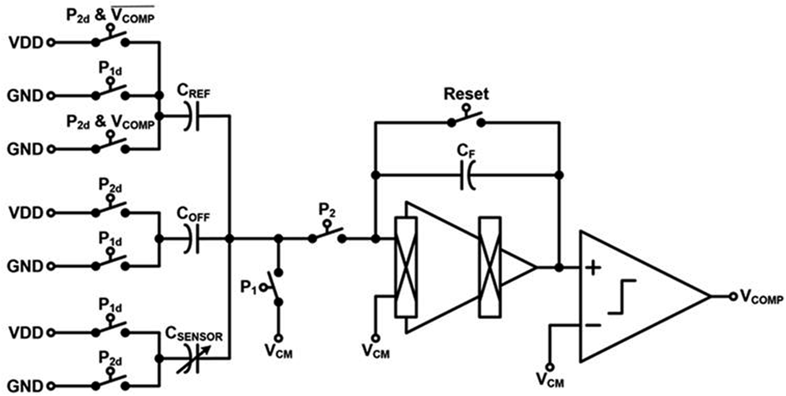
However, the delta–sigma CDC that uses the conventional chopper stabilization technique contains residual offset due to the non-ideality of the chopper switch.
The SC integrator with conventional chopper stabilization is sensitive to the parasitic components. The parasitic capacitance components connected to the chopper can degrade the effective number of bits (ENOB). 12
Moreover, the switching operation of the input chopper forms a SC resistor, and this SC resistor leaks the integrated charge from the feedback capacitance, CF. The leakage current due to switching operation of the input chopper acts as an input current noise sources. 13
The schematic of the proposed incremental first-order delta–sigma AFE with capacitor polarity swapping is shown in Figure 3. Proposed first-order delta–sigma capacitance-to-digital converter with capacitor polarity swapping technique.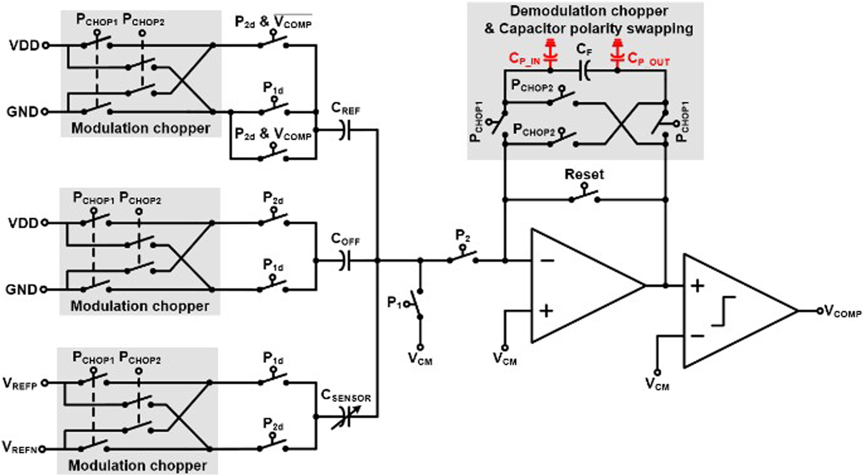
In this work, a demodulation chopper is implemented in the feedback path, which is parallel to feedback capacitor of the SC integrator. The low-frequency noise reduction effect of the demodulation chopper is similar to the conventional chopper stabilization. Additionally, the demodulation chopper can reduce the input leakage current by removing the input chopper of the amplifier.
Moreover, the parasitic capacitances at the top plate and the bottom plate of the feedback capacitance, CF, can be averaged out by the feedback chopper operation, thus, the demodulation chopper can suppress the gain and sensitivity error due to the parasitic capacitance.
All functional blocks, including the analog circuits (bandgap reference, voltage reference, and delta–sigma CDC) and digital blocks (accumulator and timing generator), are fully integrated on a chip. A reference voltage such as VREFP or VREFN is generated from the bias block consisting of the bandgap reference and voltage reference, and the generated reference voltage is used to drive the capacitive microsensors. The timing diagram of the incremental delta–sigma AFE is shown in Figure 4. Timing diagram of the incremental delta–sigma analog front end.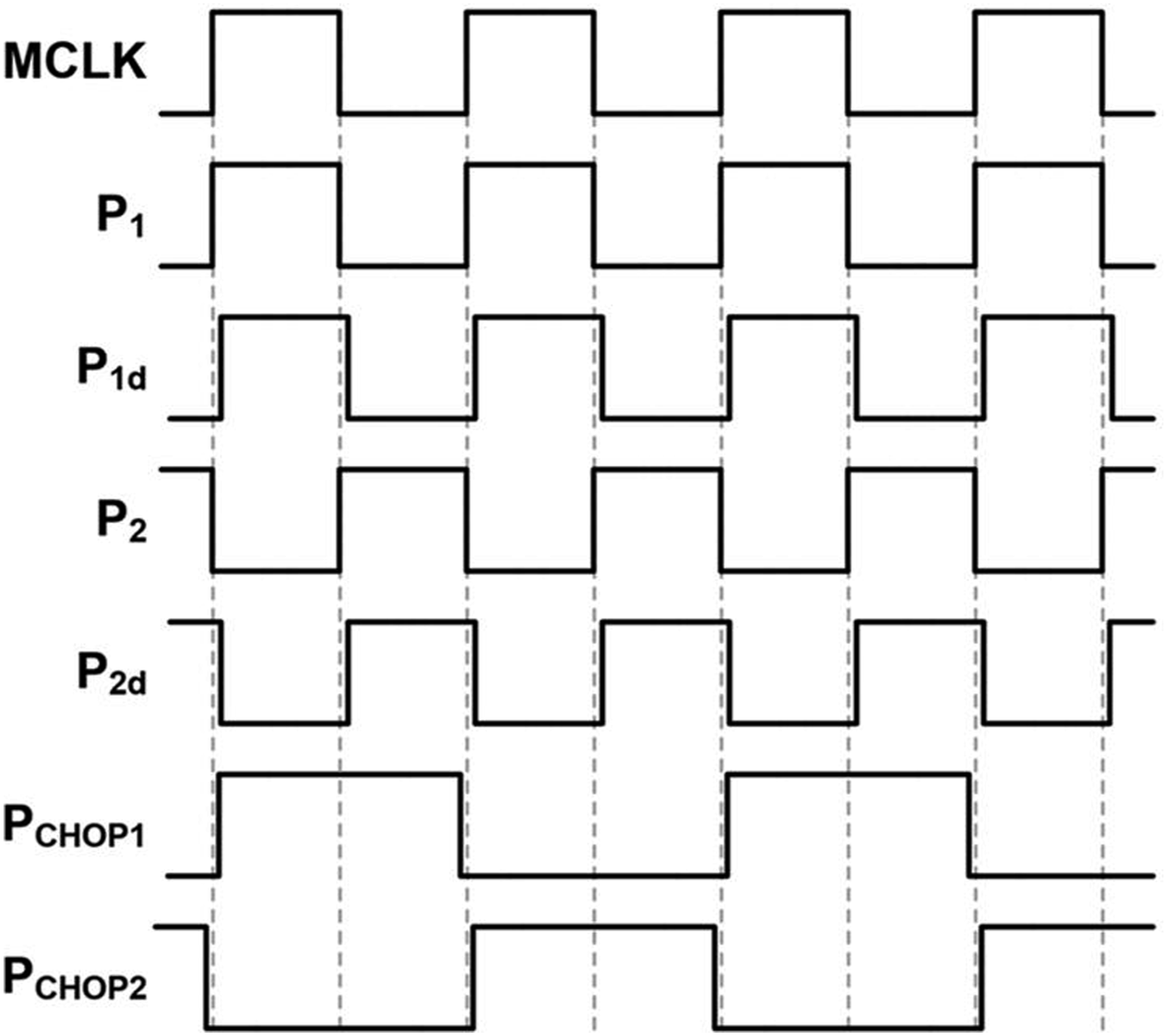
The timing generator receives an external clock to generate internal clocks. The default oversampling frequency is 500 kHz. The edges of all internal clocks are non-overwrapped.
The delta–sigma CDC operates so that the average charge of the input capacitive sensor (CSENSOR) and reference capacitor (CREF) delivered to the feedback capacitor (CF) of the integrator is zero. Offset capacitor (COFF) is also present for offset cancellation. The capacitors, CF, CREF, and COFF are digitally programmable. When switched from the P1 to the P2 phase, the charges stored in each capacitor are transferred to the feedback capacitor of the integrator. The bitstream signal generated by the comparator is converted into a 16-bit signal by a low-power digital accumulation filter.
VDD and ground are alternately used as driving voltages for CREF and COFF. VREFP and VREFN are used as driving voltages for CSENSOR.
The charge transferred to CF of the integrator when switched from the P1 to P2 phase is expressed as
The input capacitance range of the proposed delta–sigma AFE is determined by (2) and (3).


When VCOMP is “H” and ∆VOUT is less than zero, the minimum value of VOUT can be calculated.
When VCOMP is “L” and ∆VOUT is greater than zero, the maximum value of VOUT can be calculated.
The capacitive input range can be defined as

VREFP and VREFN are adjustable in the bias block, and the difference between the two reference voltages can be set up from VDD/2 to VDD/16. The proposed delta–sigma AFE is designed to measure up to 140 pF in a small active area by adjusting the reference voltage.
Experimental results
The incremental delta–sigma AFE is fabricated in a 1-poly/6-metal 0.18-µm standard CMOS process. The size of the analog and digital blocks, including the bandgap reference, delta–sigma CDC, and accumulator, is 0.42 mm2.
The current consumption of bias block, integrator, comparator and timing generator is 161.1 µA, 125.4 µA, 51 µA, 53.5 µA. The total current consumption is 340 µA from a 3.3 V supply.
The measurement environment of the proposed incremental delta–sigma AFE is shown in Figure 5. Measurement environment of the proposed incremental delta–sigma analog front end.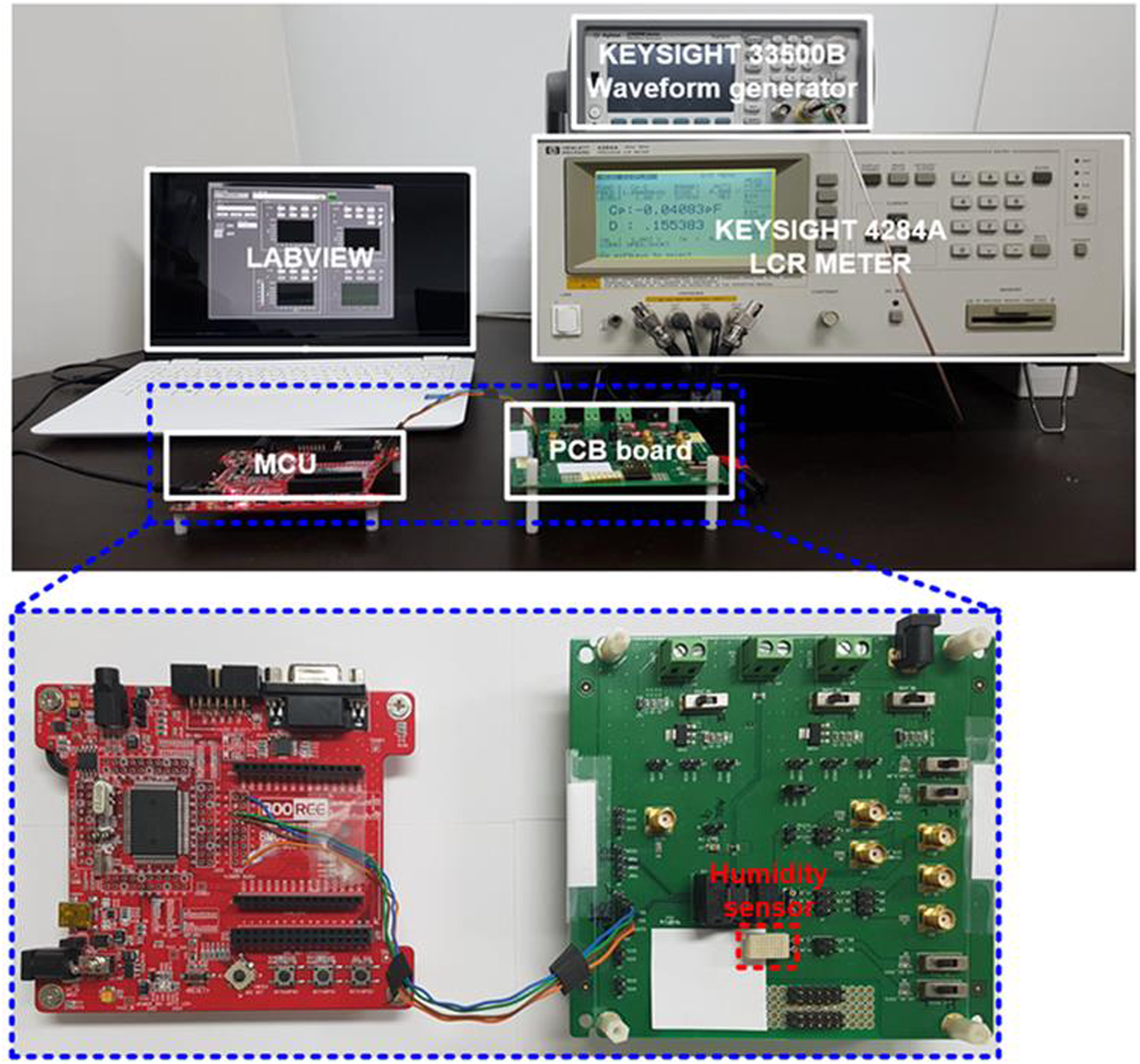
A LABVIEW program is used for data acquisition. The digital code output from the accumulator is transferred to LABVIEW through the micro controller unit (MCU), and fast Fourier transform (FFT) analysis is performed. An LCR meter is used to measure the exact capacitance value of the sensor and chip capacitor applied to the delta–sigma AFE.
Figure 6 shows the reduction in the low-frequency noise using the chopper stabilization technique. The blue and red lines show the FFT analysis results of the output code with and without implementing the chopper stabilization technique, respectively. The FFT analysis is performed on 2500 samples and Hanning window. As shown in Figure 6, the low-frequency noise is reduced by approximately 20 dB using the chopper stabilization technique. The input capacitor is fixed to a 5-pF chip capacitor. In order to analyze the noise of the proposed CDC only, excluding switching noise, charge injection, and clock feedthrough caused by the change of input capacitance, the input capacitor was fixed at 5 pF. Comparison of the measured output spectrum of the delta–sigma analog front end with and without using the chopper stabilization technique.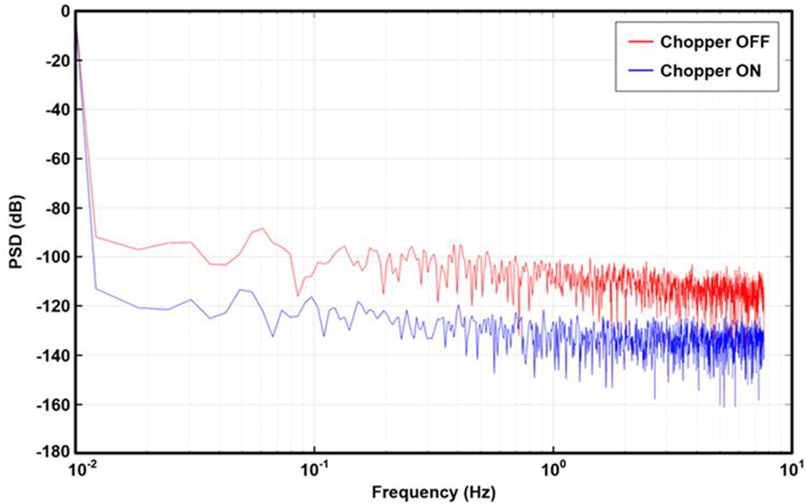
Figure 7 shows the measured accumulator output code error and histogram with and without the chopper stabilization technique. Figure 7(a) shows the output code error without the chopper stabilization technique when the data of the 2500 samples are measured. The histogram of the measured data is shown in Figure 7(b). The output code error with the chopper stabilization technique when the data of the 2500 samples are measured is shown in Figure 7(c). The histogram of the measured data is shown in Figure 7(d). The upper graph in Figure 7 shows a peak-to-peak noise of ±40 code variation without using the chopper stabilization technique. Figure 7(c) shows that the output code variation using the chopper stabilization technique is measured as ±3 code. The root-mean square (rms) noise is reduced from 11.88 code variation to 0.88 code variation when the chopper stabilization technique is used. Measured output code error and histogram without and with the chopper stabilization technique.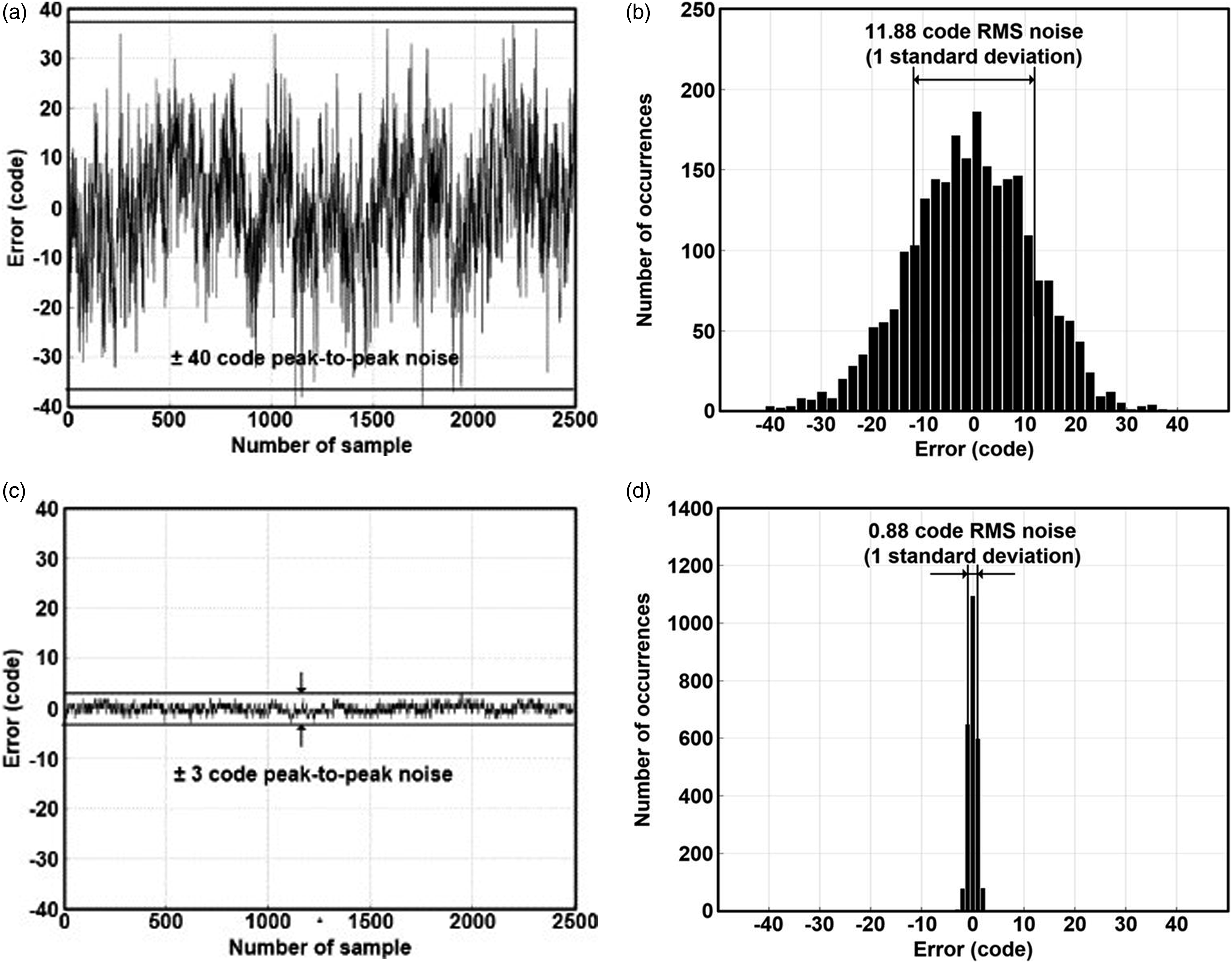
The rms noise represents one standard deviation. 9 The effective resolution is calculated from the histogram using (5), and noise-free resolution is calculated using (6). 14 The effective and noise-free resolution values of the proposed incremental delta–sigma AFE using the capacitor polarity swapping technique are 16.2 and 13.4 bits, respectively. 15–18
The measurement results of the proposed incremental delta–sigma AFE with a chip capacitor and humidity sensor are shown in Figure 8. The real capacitance of the chip capacitor used for the measurement was obtained using the LCR meter.
19–22
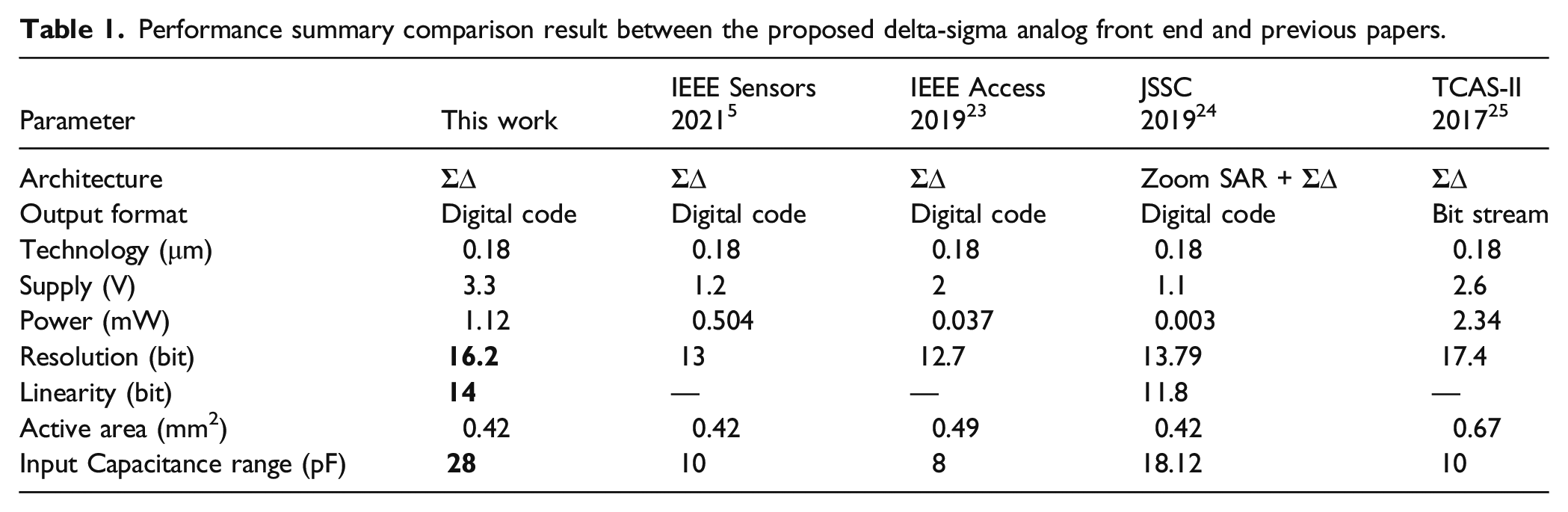
The linearity of the digital output code was measured while the input capacitor was increased from 2 to 20 pF. The measured non-linearity was 0.05% full-scale output (FSO). The measured digital output code at the input of the humidity sensor with nominal capacitance of 120 pF is shown in Figure 8(b). When the humidity was varied from 30% to 80% at room temperature using a humidity chamber, large capacitance of 120 pF was successfully measured without an additional external capacitor. Table 1. summarizes the performance of the proposed low-noise incremental delta-sigma AFE with those of previous studies [5,23,24,25]. The proposed delta-sigma AFE has wide input capacitance range. also, it has high resolution and linearity more current than those of other studies. Measurement results of the proposed incremental delta–sigma analog front end with (a) input chip capacitor from 2 to 20 pF and (b) humidity sensor with 120-pF nominal capacitance. Performance summary comparison result between the proposed delta-sigma analog front end and previous papers.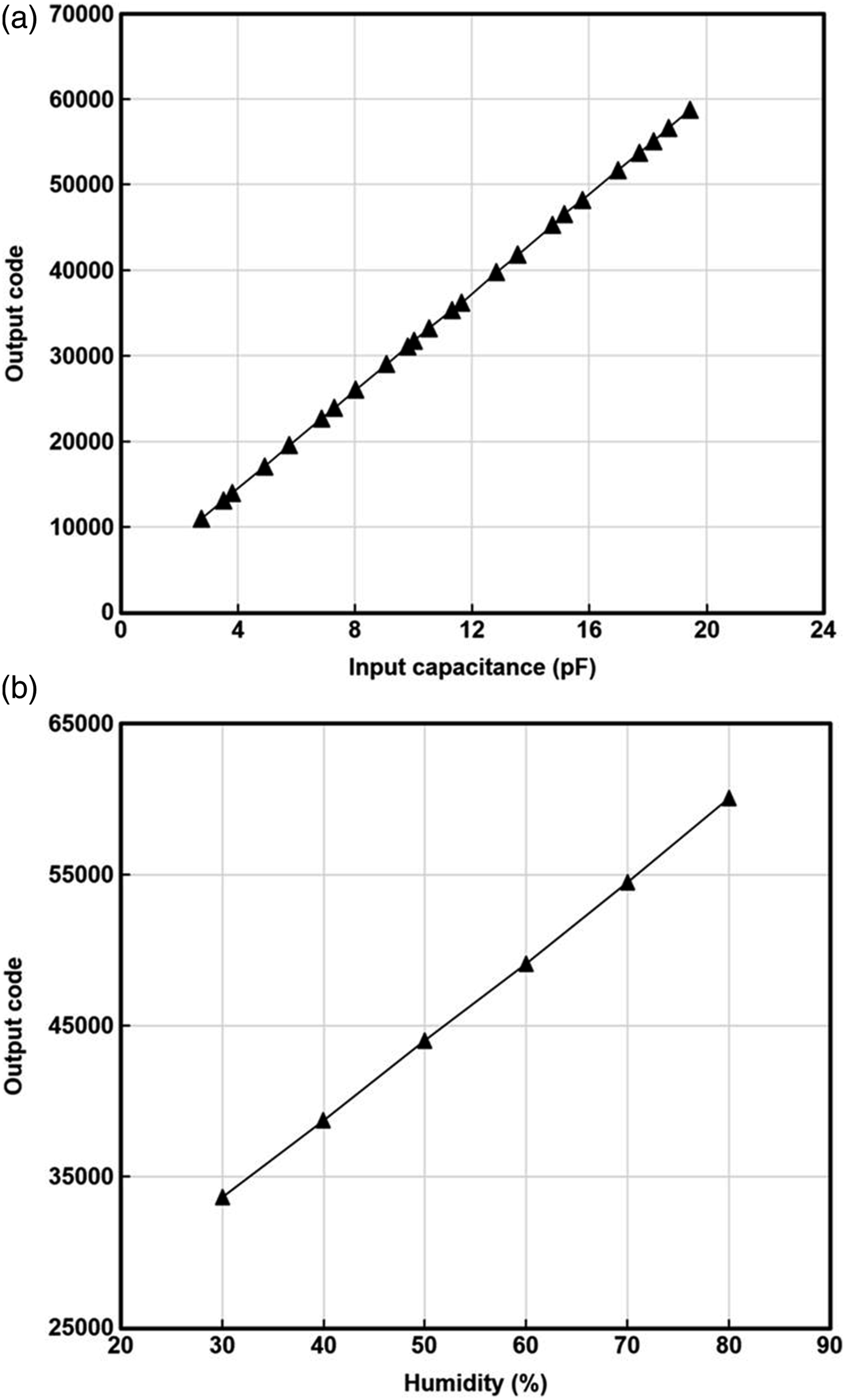
Conclusions
This paper has presented a low-noise incremental delta–sigma AFE with capacitor polarity swapping technique for capacitive microsensors. The proposed AFE consists of voltage reference, current reference, 12C interface, timing generator, first order delta-sigma modulator and 16-bit accumulator. The designed delta–sigma AFE can measure various capacitive sensors up to 140 pF. To achieve low noise and high linearity, the capacitor polarity swapping technique and chopper stabilization technique were used in this study.
The prototype IC was fabricated in a 0.18-µm standard CMOS process. The active area of the proposed delta–sigma AFE was 0.42 mm2, and total operating current was 340 µA from a 3.3-V supply.
The proposed AFE were achieved high input capacitance range 0 to 28 pF, highly effective resolution of 16.2 bit and low non-linearity of 0.05% FSO. The measured digital output code at the input of the humidity sensor with nominal capacitance of 120 pF was successfully measured.
The proposed low-noise incremental delta-sigma AFE for capacitive microsensors can be applied to various smart devices through the implementation of low power, low noise, and small area. Future research will improve the power efficiency of high resolution delta-sigma CDC so that it can be applied to various battery-operated smart devices.
Footnotes
Acknowledgements
The EDA tool was supported by the IC Design Education Center (IDEC), Republic of Korea. We also would like to thank Dongkyu Song of LeoLSI, Inc. for his insightful suggestions and discussions.
Declaration of Conflicting Interests
The author(s) declared no potential conflicts of interest with respect to the research, authorship, and/or publication of this article.
Funding
The author(s) disclosed receipt of the following financial support for the research, authorship, and/or publication of this article: This research was supported by the MSIT(Ministry of Science and ICT), Korea, under the ITRC(Information Technology Research Center) support program(IITP-2021-2017-0-01635) supervised by the IITP(Institute for Information & Communications Technology Planning & Evaluation). This research was supported by the Practical Technology Development Medical Microrobot Program (R&D Center for Practical Medical Microrobot Platform, HI19C0642), funded by the Ministry of Health and Welfare (MOHW, Korea) and the Korea Health Industry Development Institute (KHIDI, Korea). This work has also supported by the National Research Foundation of Korea (NRF) grant funded by the Korea government (MSIT) (No.2022R1A2C100517011)