
Abstract

Introduction
The manipulation of liquids within a microcapillary network remains a considerable challenge in the development of miniaturized total chemical analysis systems (μTAS). Fluid manipulation can be achieved using (micro) mechanical pumps connected or integrated into the device, and by using an electric field (E) for generation of electro-osmotic flow (EOF). For glass microdevices, electro-osmotic pumping (EOP) is most attractive, since no moving parts and/or valves are required.
In its simplest embodiment, EOP in microfluidic devices involves imposing an E along the full length of the channel by immersing electrodes into open solution reservoirs situated at both ends of the channel. Electrolytically generated gases at the electrodes drift to the surface of the solution reservoirs and escape into the air.
In more complex situations, however, EOP in a subsection of a microchannel may be required. For sampling, for example, from brain tissue in living organisms, the presence of electrodes in the ‘sample reservoir’ (i.e., the brain), and thus outside the microdevice is undesirable, since potentials applied to external electrodes interfere with the sampling environment. In these cases, electrodes need to be integrated into the microfluidic device. The use of electrodes in a microchannel, however, is not trivial. Electrolytic gases get caught in the sealed microchannel and hence effectively interrupt the electric field, and thus fluid movement. A number of approaches to avoid bubble formation during spatially localized application of voltages in microfluidic networks have been reported. In one example, a 1-mm-thick poly(dimethylsiloxane) (PDMS) substrate containing the microchannel was sealed with a glass cover plate containing the electrodes. 1 Electrolytic gases formed at the electrodes dissipated through the highly gas-permeable PDMS film into the air.
An alternative method for application of the electric field is the use of a conducting barrier between the electrodes and the channel. A Nafion membrane has been presented as an interface between an open reservoir containing the electrode and a microchannel. 2 Electrolytic gases dissipate into the air via the open reservoir, while the electrical contact afforded by the membrane ensured that an E was applied to the closed microchannel. A similar approach involves the use of adjacent side channels, which are electrically connected, via porous barriers, but where fluid exchange is strongly limited. 3,4 Either the porous membrane was formed using a thin layer of potassium silicate, in or the contact was directly over the glass wall separating adjacent channels.
The three approaches mentioned above allow the creation of field-free zones in addition to regions where the field is applied. In the field-free regions, charge-independent fluid transport can be controlled by EOP elsewhere in the microfluidic system, an effect we term “electro-osmotic indirect pumping” (EOIP) to distinguish between EOP in- and outside the electric field.
In this paper, a glass microdevice for both EOP and EOIP using electrically connected side channels is presented. Electrical contact between the main and side channels is achieved by electrical breakdown of the glass barrier between these channels. Electrical breakdown for initiating liquid contact between disconnected channels has been demonstrated in PDMS devices. 5 To our knowledge, this is the first time that electrical breakdown for initiation of electrical contact between glass microchannels is presented. Cross injection by a combination of EOP and EOIP is demonstrated.
Experimental
The layouts of single channel and cross injection devices are given in figure 1a and 1b. In both designs, adjacent side channels are integrated for EOIP experiments. The side channels have a 250 μm long section parallel and close to the main channel, and are each connected to two reservoirs to enable filling of the channel with aqueous solutions. Devices were fabricated in Pyrex® 7740 wafers by wet chemical etching in 49% HF. The distance between the adjacent channels (thickness of the wall) was controlled by the etching time, as this influences the channel width by under etching. The glass wall became thinner as etching times increased, and adjacent channels approached each other. At a channel depth of 11.3 μm, the thickness of the glass wall was 8.5 μm at the top of the channel and 29 μm at the bottom. After alignment, the devices were bonded using thermal fusion bonding.
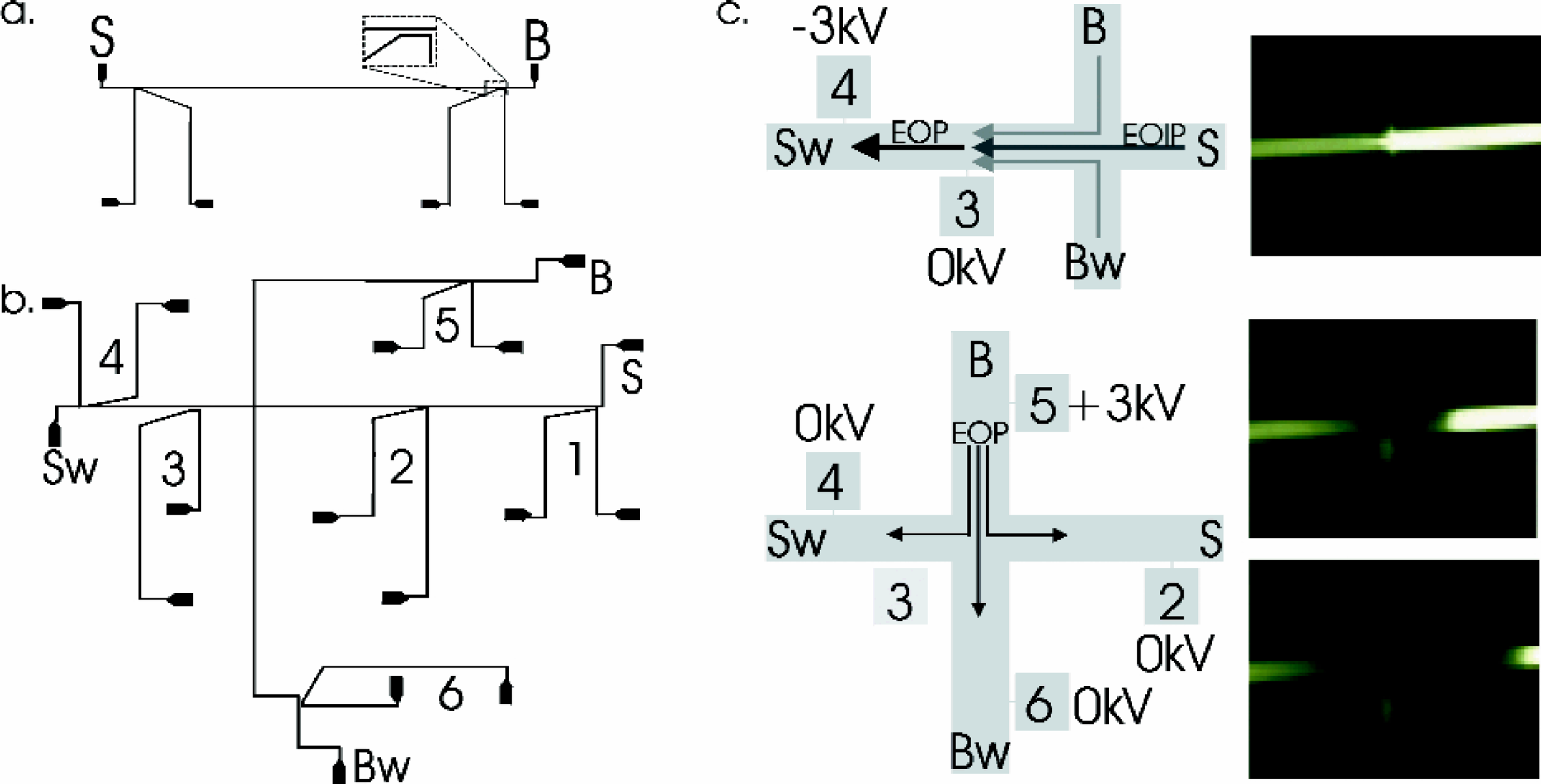
a. Layout of the single channel device. The length of channel SB was 25 mm, the glass wall thickness ∼15 μm.
Directly after the bonding, no electrical contact between the adjacent channels could be measured. For establishment of electrical contact, electrical breakdown of the glass wall separating the main and side channels was used. The electrical breakdown of Pyrex® 7740 occurs at 13.14 V/μm and the dielectric constant Hr is 4.6. The glass wall functions as a capacitor, where the effective field strength E will be proportional to E0/Hr (E0 is applied field). 6 The expected breakdown voltage of the 8.5 μm wide glass wall, assuming E to be 60.4 V/μm, is 510 V. During the breakdown procedure, all channels were filled with 1 M NaCl, and an increasing potential difference was applied between the main and a side channel. At 7 kV, electrical breakdown occurred after ∼10 seconds, and electrical contact was initiated: a current increase from 0 to > 100 μA was measured. At lower potentials, no electrical breakdown was observed, though potentials were applied for longer times (e.g. 3 kV for 1 minute). The potential required experimentally is much larger than the value expected from the electrical breakdown characteristics of Pyrex® given above. This was also observed when electrical contact was established between adjacent microfluidic channels in PDMS by electrical breakdown. 5 In our case, a couple of factors may play a role in this deviation from theoretical behaviour. Consider the system as an equivalent circuit with resistors (electrolyte filled channels) and a capacitor (the glass wall) in series. The overall applied potential required to achieve electrical breakdown of the glass wall might be increased by the resistance of the channels filled with NaCl (typically MΩ), or by a higher actual value for the capacitance. In the calculation, the glass wall thickness was 8.5 μm. This is the width at a 250 μm long section at the top of the channel, but it widens to 29 μm at the bottom of the channel, and is even thicker outside the 250 μm area. These factors will influence the breakdown process, but it is difficult to draw a direct analogy between this simple equivalent circuit model and the more complex microfluidic device. Breakdown will take place where the dielectric material is weakest, thus at etching and bonding defects where channels are closest to one another.
The resistance of the electrical connection formed during the breakdown procedure was estimated at 75 MΩ (accurate current measurements were not possible), comparable to the resistance of a 1 cm long channel (11 μm deep, 42 μm wide across the top) filled with 32 mM carbonate buffer. The contact resistances of all six side channels of a cross injection device, as well as the resistance of the contacts in the 14-μm and the 8.5-μm-wide wall, were in the same order of magnitude.
The breakdown process was identical for all glass devices, with the time required for electrical breakdown to occur increasing with increasing distance between the adjacent channels. The generation of the electrical contact was irreversible, and after the breakdown procedure the devices could be used for EOP experiments. At a glass wall thickness of 13 μm, no physical damage could be observed using an optical microscope, and no exchange of fluids between the adjacent channels could be measured. Electrical contact was nonetheless established during the breakdown process, indicating the formation of pores too small to be visible under an optical microscope for this microwall. At a glass wall thickness below 9 μm, however, both physical damage and fluid exchange were observed. Pores with widths up to 4 μm were formed and glass residues were deposited in channel, as constituted by visual inspection using a microscope.
Single Channel Device
The layout of the single channel device is given in figure 1a. The channel depth was 11.4 μm, the thickness of the glass wall was estimated at 14 μm. During experiments, both side channels were filled with 1 M NaCl, and the main channel SB with 32 mM carbonate buffer (pH 9.2). The sample reservoir (S) was filled with 0.5 mM fluorescein and the buffer reservoir (B) with an equal amount of buffer to prevent hydrostatic pressure effects. Platinum electrodes were placed in open reservoirs at the ends of the two side channels, and a potential difference was applied. By switching the direction of the electric field, fluorescein could be transported back and forth in the main channel. The flow rate of fluorescein in the field-free region (i.e. between the sample reservoir and the closest side channel) was demonstrated to increase linearly with the applied field. The RSD of the flow rate was 3.2% (n=6). During experiments, leakage of fluorescein into the side channels was not observed.
Cross Injection Device
The layout of the cross injection device is given in figure 1b. The channel depth was 11.3 μm, the distance between the main and side channels was 8.5 μm. All channels were filled with 32 mM carbonate buffer (pH 9.2), the sample reservoir, S, with 0.1 mM fluorescein in buffer, and all other reservoirs with an equal amount of buffer. In figure 1c, injection of a fluorescein plug into the buffer waste channel, Bw, is demonstrated. First, fluorescein is dragged into the microdevice by EOIP using side channels 3 and 4. After switching the applied potentials, fluorescein is injected into channel Bw, using the electric field applied between side channels 5 and 6. The cross injection devices had a glass wall of only 8.5 μm, and leakage of fluorescein into the side channels was observed.
Conclusions
Electrical contact between two channels was established by electrical breakdown of the intervening glass wall. Electrical contact without liquid exchange from one channel to another was observed at a glass wall thickness of 13 μm. At wall thicknesses between 8 and 9 μm, however, pores in the order of 4 μm were formed, resulting in fluid exchange over this interface. Improvement of the control and understanding of the electrical breakdown process are under further investigation.
The electrically connected side channels were used to combine EOIP and EOP for cross injection of fluorescein. EOIP allows charge-independent fluid transport in field-free regions of a fluidic network, controlled by the EOF generated in a locally applied electric field. Flowrates in the field-free regions depend on the applied E (increase with increasing E), as well as on the channel's resistance to flow, a parameter that is determined by channel geometries. The longer the channel is, or the smaller its cross sectional area, the greater will be its resistance to flow, and the smaller the EOIP rates.
One major advantage is that EOIP can be used for direct sampling without having electrodes outside the microdevice. Other applications can be found in sample pretreatment, charge-independent fluid transport, hyphenation of analysis steps and mixing of reagents with different electrophoretic mobilities.
Acknowledgements
RMG, EB and GWKD acknowledge STW, the Dutch Foundation for Science and Technology for financial support in the framework of the BIOMAS project (DST 4351).