
Abstract
Material reliability is among the crucial factors that impact the performance of devices. In order to predict material reliability, an accelerated ageing study to predict material shelf life when subjected to temperature and humidity was performed on silicon nanowires (SiNWs). We investigated the effects of process conditions on the diameter and the quality of SiNWs using Atomic Force Microscopy followed by statistical analysis. The experimental results revealed that diameter of SiNWs has a linear relationship with changing temperature and humidity. These results are of significant importance and will be a critical design consideration for the manufacture of nanoelectromechanical systems involving SiNWs.
1. Introduction
Nanowires (NWs) are one of the basic building blocks for nanoelectromechanical systems (NEMs). Many different types of NW exist, including metallic (nickel (Ni), platinum (Pt), gold (Au)), semiconducting (indium phosphide (InP), silicon (Si), gallium nitride (GaN)), and insulating NWs (silicon dioxide (SiO2) and titanium dioxide (TiO2)). Currently, research is showing tremendous interest in one-dimensional (1-D) nanostructures, such as NWs and nanotubes, due to their potential to serve as critical building blocks for emerging nanotechnologies [1–5]. Of particular importance to 1-D nanostructures is the electrical transport through these “wires”, since predictable and controllable conductance will be critical to many nanoscale electronics applications. One-dimensional nanostructures such as semiconductor NWs are attractive as building blocks for the assembly of nanoelectronics and nanophotonics systems because they can function both as nanoscale devices and interconnects [6]. Silicon nanowires (SiNWs) represent a particularly attractive class of building block for nanoelectronics because their diameter and electronic properties can be controlled during synthesis in a predictable manner [7–9]. The ability to control the electronic properties has been utilized for the reproducible assembly of field-effect transistors (FETs) [10–12], logic gates [13], and sensors [14]. In addition, recent studies suggest that SiNW FETs can exhibit transport characteristics that are comparable to or exceed the best planar devices fabricated by top-down approaches [11]. Carbon nanotubes had shown prominence in the field of one-dimensional nanostructures. However, the size dependency of electrical properties and the inability to alter the electrical characteristics through doping have limited their usage. SiNWs on the other hand, with their ability to alter electrical properties, offer flexibility and have thus been intensely studied by many researchers and scholars. However, before taking full advantage of SiNWs, it is critical to understand their reliability under environmental conditions such as temperature and humidity. Understanding of SiNWs' reliability will help facilitate the modelling of the mechanics for changes in physical and mechanical properties as SiNW-related nanosystems age.
Accelerated ageing is used in the study of material shelf life, and is often performed in laboratory settings. It is the most often-adapted test to predict the lifetime when there are no scientific data available. In this test, the material is subjected to excessive oxygen, temperature, and sunlight in order to accelerate its actual ageing [15–16]. The material properties such as mechanical fatigue, load cycle intake, and material stability are evaluated for the prediction of the shelf life of the material. Though Europe has favoured standard testing methods based on ageing at elevated temperatures, slicing and scaling techniques have been the leading approach in North America [17]. Recently, standard test methods in Canada have been adapted by many industries across the US, but these test methods are only defined for the macroscale components. As the test methods involve slicing the material [18–22], which is impossible at the micro- and nanoscale levels, these methods cannot be directly adapted for micro- and nanoscale materials.
Accelerated ageing testing is based on a thermodynamic temperature coefficient formulated by Von't Hof, which states that “for every 10 degree C rise in temperature the rate of chemical reaction will double”. However, since this formulation is based on rate kinetics of a single chemical reaction, not on packages with various kinds of material, direct extrapolation of this theory to the ageing of packaging materials must be used with caution.
In order to overcome the above shortcomings and to predict the reliability of SiNWs, a new accelerated ageing experiment was carefully designed and tested based on Taguchi's approach [23–29] for nanomaterials. Using this designed experimentation scheme, SiNWs' reliability was studied by subjecting them to varying temperatures and relative humidity (RH), and their dimensional changes (diameter) were recorded using an Atomic Force Microscope (AFM). Statistical analysis was performed on the data collected to enable a reliability study and facilitate the modelling of the mechanics for changes in physical and mechanical properties as SiNW-related systems age. Different researchers have worked with SiNWs in high temperature or humidity. According to the morphology and 3D images in these papers, it is shown that silicon oxide leads to an increase in SiNWs' diameter [30–32]. In this paper, we try to find the relationship between this oxide growth and the temperature and humidity.
2. Materials and Method
SiNWs (>99%) and acetone (>97%) were purchased from Sigma Aldrich. 40 mg of SiNWs was measured out using an electronic balance with a resolution of 10 μg and suspended in 1 mL of acetone to make a seed concentration of 40 mg/mL. From the seed concentration, the final working concentration of 0.1 mg/mL was prepared by mixing 250 μL into 1 mL. In order to ensure a uniform dispersion, the seed solution was sonicated in a sonicator for 1 hour at 42 kHz ± 6% with 85 W, and then the final working concentration was prepared. The final working concentration was again sonicated for 1 hour and then dispersed onto the glass slide. The acetone was evaporated using a hotplate. The SiNW-dispersed glass slides were then subjected to variable temperatures at a constant humidity and at variable humidity with constant temperature. A Microclimate Environmental Chamber (manufactured by Cincinnati Sub Zero, model no. MCBH 1.3) was employed for the study. In the first part of the experiment, keeping the relative humidity constant at 3% RH, the temperature was ramped between 22°C and 150°C with a step increment of 10°C for 30 minutes. In the second part, the temperature was kept constant at room temperature and the relative humidity varied between 20% RH and 90% RH with a ramping of 10% RH. The samples were then analysed for dimensional changes using Atomic Force Microscopy (AFM). The AFM was utilized to obtain surface images of the treated SiNWs. The changes in the dimensions of the SiNWs were recorded.
3. Experiments: Dimensional Analysis Using AFM
The initial diameters and lengths of the silicon NWs before exposure to the environmental chamber were 40 nm and 1–20 μm respectively for 99% of the SiNWs. The melting point (mp) of the SiNWs was 1410°C. In order to accurately determine the diameter of the treated SiNWs, an AFM was employed. The AFM used in the experiment was the highly sensitive and precise Agilent 5500-ILM microscope. The scanning and characterization were done under Acoustic AC (tapping) imaging mode. The AFM probe utilized during imaging had a resonant frequency of 190 kHz and a spring constant (Fc) of 48 N/m. During intermittent contact, the tip was brought close to the sample so that it lightly contacted the surface at the bottom of its trajectory, causing the oscillation amplitude to drop. Hence, the influence of the cantilever tip during the dimension measurement can be neglected since it did not change the shape in this mode of contact.
A small scanner (max. scan size 9 μm × 9 μm) with aluminium (Al)-coated tip was used for scanning the samples. Prior to the experiments, the tip sensitivity was calculated. The sensitivity (S) of the tip was the ratio of deflection of cantilever to the applied amplitude. The tip was calibrated for sensitivity with respect to a mica surface; the sensitivity was 66.4 nm/V. A set point voltage (V) of 0.4 V was used for the accelerated ageing study. Thus, the applied tip force F was obtained as 1.275 μN using Equation (1). The SiNW samples were then loaded into the AFM for scanning and measurement of the diameter changes. In order to maintain the surface integrity, the AC mode (Non-contact/Intermittent Contact) scanning was used.

At first, in order to locate the SiNWs, a large scan area of 4 μm × 4 μm was scanned. The scan areas of the SiNWs before and after environmental chamber treatment are shown in Fig. 1 (a) and (b). As depicted in Fig. 1, NWs were spread all over the glass plane. Once the NWs were located, a traverse was drawn across each one in order to obtain a two-dimensional graph. A traverse generated from the AFM is shown in Fig. 2. The dimensional data can be obtained from the graph. According to Fig. 2, the lateral size of a sample SiNW is more than 500 nm, which is larger than the true diameter of the SiNWs; this is because of the effect of the tip size and shape and feedback parameters. The SiNWs' height is about 60 nm, which is directly related to the true SiNW diameter after treatment.
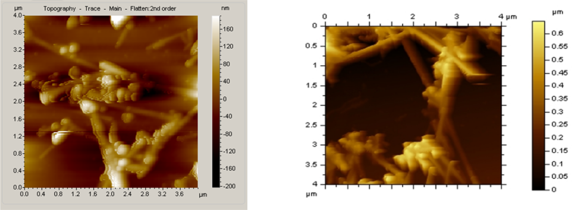
Surface images after sample prep and prior to treatment (left) and after treatment (right)

Traverse of the dimensional data generated from AFM
4. Results and Discussion
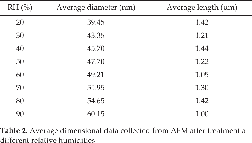
To further understand SiNWs, as shown in Fig. 3, 3D images were generated using Pico image software. In order to obtain precise and accurate results, dimensional data of 20 NWs were collected and then averaged. The average length and diameter of the SiNWs after exposure to the environmental chamber, i.e., to temperature and humidity, are given in Tables 1 and 2, respectively. The plots of the data with error bar in these tables are shown in Figs. 4 and 5, respectively. In Figs. 4 and 5, the R2 (coefficient of determination) values provide a measure of how well future outcomes are likely to be predicted by the linear models. The closer the values are to 1, the better the model. In these experimental results, the values are extremely close to 1, hence the models can be used to predict future outcomes. The measured diameter results are based on 20 measurements for temperature at 100°C and relative humidity at 80%. From Tables 1 and 2, it can be seen that the diameters changed with ageing treatments. However, the diameters appeared to decrease initially but consistently increased with temperature and relative humidity. It appears that the diameters of the SiNWs have a linear correlation to temperature at a constant humidity and a linear correlation to relative humidity at a constant (room) temperature.
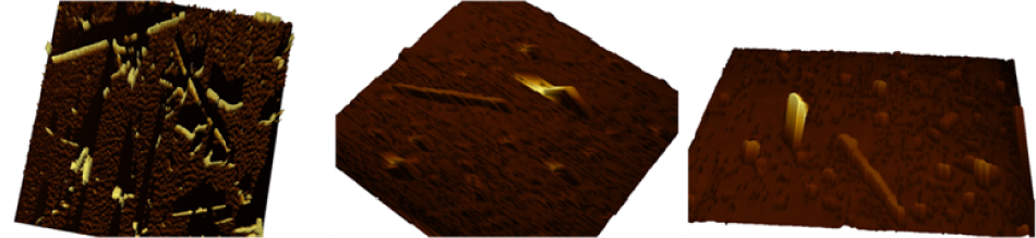
AFM 3D images after treatment

Average diameter of the SiNWs as a function of temperature
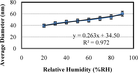
Average diameter of the SiNWs as a function of relative humidity
This is important because the material properties at nanoscale are size- and shape-dependent. While the diameter of the SiNWs is the same for all NWs (>99% have a diameter of 40 nm), the length varies in the range of 1–20 μm. Thus, no conclusions can be drawn on the length changes. However, based on the current experimental results (Tables 1 and 2), it can be concluded that the length of the SiNWs is no more than 1.5 μm.
Average dimensional data collected from AFM after treatment at different temperatures

Average dimensional data collected from AFM after treatment at different relative humidities
5. Statistical Analysis
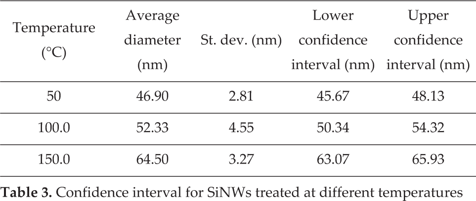
In experiments like these with high data acquisition, statistical analysis is of pivotal importance. In statistics, confidence interval (CI) is an interval estimate of the overall population. It can help to define the population more accurately by assigning a range which includes the mean of the population. This is usually calculated based on the mean and standard deviation of the population. The range varies based on the percent of the population that should be included. In general, for a huge data set, 95% population inclusion will be a very good estimate. Hence, we calculated the CI for 95% population utilizing Equation (2).

where X̅ is the mean values of the samples, Z, the critical value, is equal to 1.96 in a 95% CI, σ is the standard deviation, and N is the number of samples, which is equal to 20 in this experiment. The CIs for the SiNWs exposed to three different temperatures and relative humidity points are given in Table 3 and Table 4, respectively.
Confidence interval for SiNWs treated at different temperatures
Confidence interval for SiNWs treated at different relative humidities
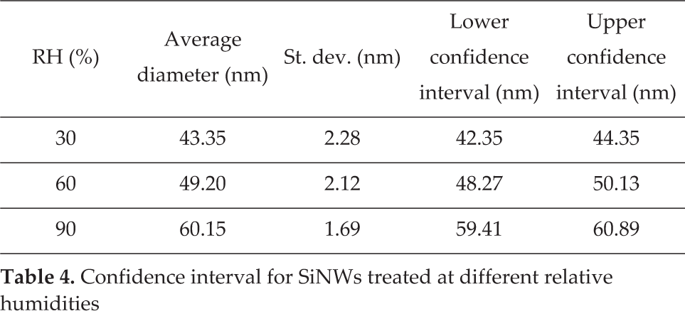
For both temperature and relative humidity exposure, the range of the diameter is within 10 nm, showing the precision of the measurements made with the Atomic Force Microscope.
6. Conclusion
The material dimensions at the nanoscale have significant impact on the material's properties. The SiNWs are used in various devices such as SiNW-based sensors [33] and high-performance SiNW FETs [34, 35]. These devices need to work in different environmental conditions such as high temperature and high humidity. In addition, they are sensitive to SiNW diameter. For example, the sensitivity, response time, and recovery time of these sensors are related to the diameter of SiNWs. The present study has studied the reliability of the SiNWs under different conditions of temperature and relative humidity.
Use of NWs leads to significant improvement of fabrication of nanodevices like nanosensors. While these devices are fast and exact, they are also more sensitive to environmental conditions. For example, when SiNWs used in a nanosensor are exposed to high temperature or humidity, a shell of silicon dioxide will cover the SiNW core. Oxidization of SiNWs may form a dielectric shell in electronic devices at the nanoscale and affect such devices' properties.
The current results confirm the need to make the necessary design considerations when SiNW-based devices are researched in conditions of variable temperature and relative humidity, as the material dimensions at the nanoscale have significant impact on the material's properties. The present study also concludes that the SiNWs' diameter has a linear relationship with respect to temperatures in the range of 22°C–150°C and a linear relationship with respect to the relative humidity. This also indicates that the cause of the NWs' increase in diameter after temperature treatment is likely oxidation. After humidity treatment, the NW diameter does not return to previous sizes. This may indicate that the increase of diameter may not be due to moisture absorption. Further research is needed to model the mechanics of changes in physical and mechanical properties as the systems age.
Footnotes
7. Acknowledgements
This work was funded by National Science Foundation (Grant Number: ENG-EEC-1005201).