
Abstract
Modification of the electrical transport of a random network of silicon nanowires assembled on n-silicon support, after silicon nanowires functionalization by chlorination/alkylation procedure, is here described and discussed. We show that the organic functionalities induce charge transfer at single SiNW and produce doping-like effect that is kept in the random network too. The SiNWs network also presents a surface recombination velocity lower than that of bulk silicon. Interestingly, the functionalized silicon nanowires/n-Si junctions display photo-yield and open circuit voltages higher than those including oxidized silicon nanowire networks. Electrical properties stability in time of junctions embedding propenyl terminated silicon nanowires network and transport modification after secondary functionalization is also shown. These results suggest a possible route for the integration of functionalized Si nanowires, although randomly distributed, in stable large area photovoltaic or molecule sensitive based devices.
1. Introduction
Silicon nanowires (SiNWs) have been the subject of an extensive research addressed to explore all their possible applications from the solar energy conversion to sensing. [1–3] SiNWs have been also widely used as building block of the next generation solar cells and high mobility field effect transistors (FETs).[3–8] The advantage of integrating single, arrays or networks of SiNWs in solar cells, is the possibility of decoupling the light absorption from the charge transport of the minority carriers whose lateral diffusion is one order of magnitude lower (hundreds of nm) than that observed in bulk Si (> 1 μm).[6,9,10] Furthermore the enhanced optical absorption from ultraviolet to near infrared optical range could result in a higher efficiency of the Si NW based device. [9] Recently, the requirement of large scale deposition of silicon nanowires for potential application in microelectronics system like displays, biological and chemical sensors, and also large area solar cells has lead to focus the attention on networks of randomly oriented SiNWs.[1,11,12] Furthermore the lower temperature processing with respect to single Si crystal allows the deposition on plastic flexible substrates.
It is noteworthy the observation that in a single SiNW the surface to volume ratio larger than in Si bulk, although advantageous, implies that the surface states as dangling bonds, defects or adsorbates play a more relevant role that could affect the device performances. Also, the silicon dioxide (SiO2) coating SiNWs is thought to induce trap states at the SiO2/Si interface increasing surface carrier recombination. [13] This has been shown to limit, for example, the possibility of controlling the channel conductivity in SiNWs based FET devices. [7] The use of H terminated SiNWs gave results unstable in time due to subsequent oxidation under air exposure. [13] However, the high SiNWs surface reactivity allows their chemical manipulation resulting in a desired change of transport properties. [14] With respect to H and SiO2 terminated–SiNWs, non-oxidized methyl (CH3-) terminated SiNWs displayed increased mobility and allowed to achieve FET devices on-off ratio higher than 105 together with chemical stability in time.[15] Although CH3 termination is quite stable in air and ensure a good coverage of the top Si atoms, subsequent bonding of organic functionalities is not allowed. Recently, intrinsic (undoped, 1015-1016 cm−3) SiNWs have been covalent bonded via Si-C to different molecules (methyl, propenyl and propynil) by chlorynation/alkylation processes. Specifically, it has been shown that propenyl scaffold lead to both full coverage of the Si sites and are capable of further functionalization. [15,16]
This work aims to enlighten on the electrical transport properties of junctions built with a random network of the above mentioned functionalized SiNWs (RN-SiNWs) self assembled on a silicon support. Evidence of the further carrier transport modification across a similar junction including random network of subsequently functionalized propenyl –SiNWs is also presented.
2. Experimental
2.1 Si NWs fabrication
The SiNWs random network under investigation have been prepared on highly doped n-Si(111)(Sb doped, 1018/cm3) starting from intrinsic SiNWs (1015-1016 /cm3) prepared by vapor-liquid-solid growth mechanism using chemical vapour deposition with silane. After being cleaned (N2 flow), hydrogen-terminated Si samples were prepared by etching the amorphous SiO2 coating, then exposing the SiNWs to buffered HF solution (pH=5) for 40 s. The samples were then removed and rinsed in water to limit oxidation, dried in flowing N2(g) for 10 s, and immersed into a saturated solution of PCl5 (99.998%, Alfa Aesar) in C6H5Cl (0.65 M) that contained a few grains of C6H5OOC6H5 to act as a radical initiator. The reaction solution was heated at 90±10 °C for 10 min. The chlorinated samples were rinsed with tetrahydrofuran (THF) and the samples were transferred to a N2-purged glove box. While being in the glove box, the chlorinated samples were immersed for 12–24 hrs (in the case of Si NWs) in a THF solution of 3.0 M methylmagnesium chloride (CH3MgCl) at 120±10 °C, 0.5M 1-propenylmagnesium bromide (CH3-CH=CH-MgBr), or 0.5 M 1-propynylmagnesium bromide (CH3-C≡C-MgBr) for producing alkyl terminated Si samples. Alkylated samples were either: (i) rinsed with THF, methanol and transported out of the glove box and further rinsed with DI water, and dried under a stream of N2(g); or (ii) sonicated for ca. 10 min in the same solutions and dried under a stream of N2(g). The alkylation process was gentle in the sense that it neither damaged (or broken) the Si samples nor changed the dimensions of as-grown Si NWs. The subsequent propenyl-Si NWs functionalization with photoactive aryldiazirine cross-linker (TDBA-OSu) was performed by placing functionalized SiNWs in a 10-mm quartz cuvette. Then the solution was added and immediately illuminated with a broadband UV lamp. The samples were then rinsed vigorously with CCl4, CH2Cl2, and water. The Para-Phenylenediamine (PPD) deposition on TDBA-OSu-CH2-CH=CH-Si NW was performed by placing the TDBA-OSu-CH2-CH=CH-Si NW in a solution of pra-phenylenediamine (PPD) in DMF. After immersion for 2 h, the samples were cleaned by rinsing with DMF and CH2Cl2, and dried by N2(g) flushing.[15,16] Figure 1(a-b) displays a typical top view (1a) and cross sectional scanning electron micrograph (1b) of a SiNWs random network fabricated on the n-Si substrate. The average SiNWs length, roughly corresponding to the thickness of the SiNWs random network, was estimated around 2 μm, while the single SiNW had an estimated average diameter of 50 nm.
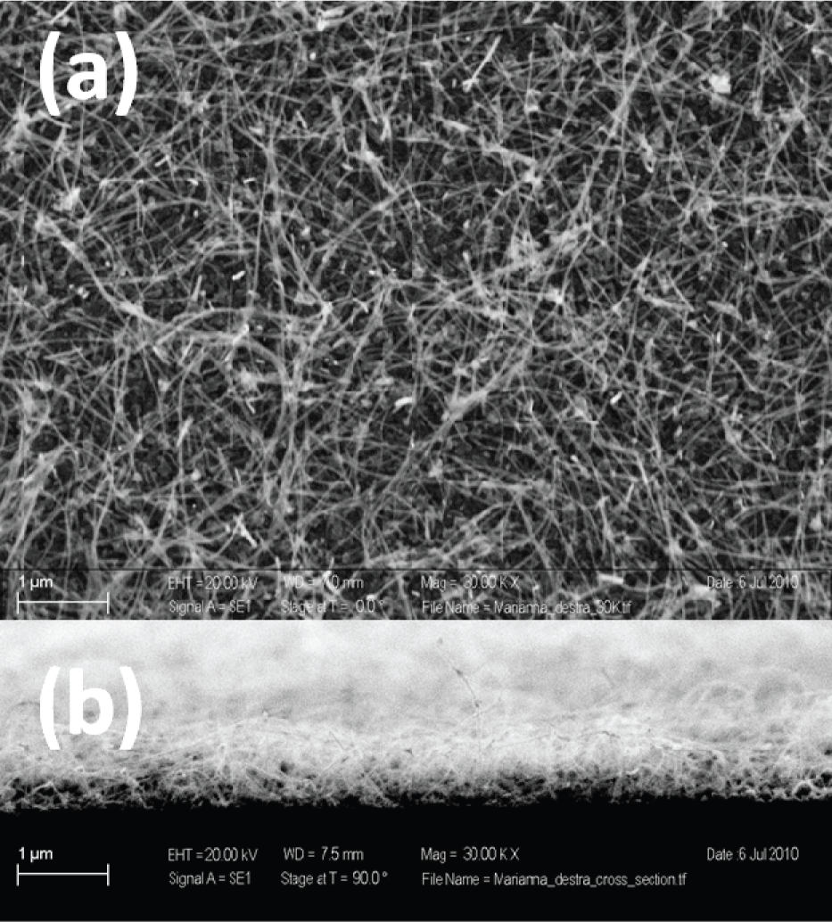
Typical top view and cross sectional SEM images of SiNWs random network on (Nd∝c1018/cm3) (111) n-Si substrates. SiNWs were prepared by the vapour-liquid-solid (VLS) method using chemical vapour deposition with silane and then terminated with different organic molecules using a chlorination/alkylation process (see ref.15 and 16)
2.2 Electrical measurements set up
A typical configuration for electrical characterization on functionalized RN- SiNWs on nSi is displaced in the Figure 2. A gold slab (2×2 mm2) has been mechanically placed on the top of the random network and used as top contact to avoid any effect of gold contact evaporation on NWs (e.g. gold penetration in the random network), as well as some possible damage on organic termination

Schematic of the device configuration used for optoelectronic characterizations. A gold slab has been used instead of evaporated gold while InGa past has been painted on the back side of n-Si wafer for ohmic contact formation. The orange arrows is a simplified representation of the current percolation paths.
The dark current (J) and photocurrent (Jph) characteristics as a function of the applied bias V (J vs V, Jph vs V) were collected in air and at room temperature by using an electrometer and a voltage supplier. The open circuit voltage values Voc have been extracted from Jph vs V curves too. The photo-efficiency conversion Yph of the devices was measured by detecting the short circuit current using the electrometer during a t=60 s continuous white light pulse provided by a 70 W halogen lamp (power density of 100 mW/cm2). The Yph vs t values have been determined for each structure by subtracting the corresponding dark current density Jdk (i.e.current detected before light on) from the total short circuit current Jsc and then by normalizing to the dark current density i.e. Yph= (Jsc- Jdk) / Jdk. It is worth remarking that the negative value of the detected current at zero bias, confirms the presence of a photovoltaic behaviour in the full set of the examined devices.
A mapping of the junction J vs V (J, dark current), Jph vs V (Jph, photocurrent) characteristics, open circuit voltage, Voc and photo-efficiency Yph vs t, has been performed by placing the gold slab at different positions on the NWs layer surface. This procedure allowed to evaluate both the uniformity of organic molecule termination effect on RN-SiNW on the junction transport properties and to account for the SiNWs surface density on silicon support. The reported J vs V, Jph vs V, Yph vs t curves and Voc values results therefore from the average of the values extracted from the collected characteristics at the different positions of the Au slab.
The transient photoconductivity measurements have been performed by using the contact configuration shown in Fig. 2 and using the λ=590 nm of a pulsed Dye laser light (repetition rate 10 Hz, τ=9ns, energy of tenths of nJ per pulse, laser spot diameter 2 mm). The laser has been gently focused onto the SiNWs random network side in a region very close to the Au slab. This position has been chosen in order to avoid laser screening or reflectance effects due to the Au slab. The Jph signal is measured at zero bias in mV on the 1 MΩ input resistance of a Lecroy digitizing oscilloscope. The data have been then normalized to the maximum detected current and the decay times (τ) have been obtained by the exponential fit of the photoconductivity signal averaged over 1000 shots.
3. Results and discussion
Figure 3 shows the comparison between the averaged JvsV characteristics performed on RN of (SiO2-SiNWs)/n-Si and on RN of functionalized SiNWs/nSi junctions.

JvsV characteristics collected on RN of SiO2 and molecularly functionalized SiNWs array on n-Si junction.
The good packing density of the SiNWs, also evidenced by SEM analysis, can be further deduced by the decrease of the detected current across the junction of around two orders of magnitude with respect to that measured under the same experimental conditions (Au slab) on bare degenerated n-Si (data not shown). Interestingly, a general increase of the forward current has been detected for junction embedding functionalized SiNWs RN compared to those including SiO2- SiNWs ones. The results furthermore show a slightly higher rectification ratio in junction embedding methyl and propenyl terminated SiNWs RN, rather than in those including propynil -SiNWs RN.
For all the structures embedding RN-SiNWs, the averaged forward bias JvsV characteristics display a power law dependence J vs Vn with 1.4<n<2 depending on the molecular terminations. Therefore, a percolative mechanism is responsible for the conducting path across the SiNWs sandwiched between the top and bottom electrode [17,18]. Specifically, the n-value goes from that of a super-linear regime (1.4, for CH3-SiNW) to that typical of a space charge limited current (2, for SiO2 and propynil -SiNWs). Moreover, other interesting features in JvsV junction characteristics can be observed.
In particular, in the as received molecular modified RN SiNWs/n-Si junction the increase of forward current with respect to RN SiO2-SiNWs/n-Si one is associated with a current onset displacement toward lower voltages. This effect, that is present notwithstanding the similar SCLC behaviour (n~2) is typically observed in single nanowires when terminated with positive dipolar molecular layer. [19,20] The positive dipole formation could be one of the effects of functionalization on each single NWs producing a charge transfer such as an electron donation from the SiNWs to the molecule.[20] This effect is due to a decrease of the electron carrier concentration and then a downward shift in the SiNWs Fermi level position. Conversely, this implies a modification from intrinsic-like to a more p-type-like character of each NW. [20] Interestingly, the molecule termination effect is detectable also when SiNWs are arranged in a random network probably because of the high SiNW density. As a matter of fact, the p-type character of the molecularly functionalized SiNWs RN is also clearly evidenced by the increase of the junction rectification ratio compared to that encountered in the junction embedding the SiO2-SiNWs RN. The latter behaviour can be ascribed to the similar n-like character of the network and n-Si support.
However, the current onset displacement (indicating the magnitude of the p-type doping of SiNWs network) does not strictly follow the increase of the theoretical dipole of SiNW molecular termination. In fact even if the dipole values are 0.8D, 1.3D and 1.6D for methyl-Si, propenyl-Si and propynyl-Si respectively, the highest increase in conductivity (i.e. high p-doping like effect) has been observed in methyl terminated SiNWs.[21] The effect of the different molecular coverage of the single SiNW can be excluded, since previously reported results evidenced a nearly full molecular coverage (around 100%) for all the terminations. [15] Another possible factor reducing the current across the propenyl and propynyl -SiNWs layer could be the different tunnelling effect from the SiNWs across the molecular layer due to thickness higher than that of CH3- (2.3 Å, 5.3 Å and 5.8 Å for methyl, propenyl and propynil termination respectively).[15] However even if JvsV data are scaled to account for tunnelling effect, the trend is preserved when changing the molecule termination. Also, interface oxidation effect can be excluded since oxide on functionalized SiNWs has been detected after around 10 days and 20 days in methyl and propynyl samples respectively, while it does not occur at all in propenyl.[15] It is noteworthy to observe that in case of small NWs (50 nm diameter) dimensionality implies that surface states can strongly affect the molecule-SiNWs charge transfer effect so that mechanisms like pinning of the Fermi level at different position in the SiNWs band gap could affect the carrier transport properties. [22] Therefore, the fact that the current onset shift in propenyl and propynyl-SiNWs is lower than that in methyl-SiNWs could be explained by hypothesizing the presence of a different energy distribution of the interface states across the SiNWs gap.[22]
If this is the case, the molecule- SiNWs charge transfer effect can be limited due to the interface state density causing the pinning of the Fermi level position inside the NWs gap. As a further limiting factor of charge transfer, the different electrical field screening effect of propenyl and propynyl-SiNWs compared to methyl-SiNWs has to be taken into account. This effect can decrese the external applied electric field across the NWs leading to a reduced value of the detected current. The reason of the observed behaviour can be clarified through the examination of surface recombination velocity results below reported.
The electrical transport stability across the functionalized RN-SiNWs/nSi junction was checked by performing JvsV as soon as the samples were received (about 10 days after sample preparation) (Figure 4(a)) and one month later (Fig.4(b)) under the same experimental conditions.

Dark forward current density vs. voltage (J vs. V) characteristics of RN SiNWs/n-Si junction; in the legend the corresponding SiNWs terminations have been indicated. a) J vs.V collected soon after receiving the samples (around four days after sample preparation); b) J vsV characteristics collected one month later.
The JvsV characteristics collected after one month (Fig. 4b) show that the voltage shift of the current onset observed in propenyl –SiNWs/n-Si with respect to SiO2-SiNWs/pS, is almost the same, while it is reduced in methyl and propynil- SiNWs/n-Si. These data confirm what already observed about the high resistance to oxidation of the propenyl-SiNWs; here we also show that also the dipole induced doping-like effect is preserved [15]
Figure 5 shows the photocurrent density vs. voltage (JphvsV) related to the propenyl-SiNWs/n-Si junction along with the dark JvsV curve. The detection of the open circuit voltage Voc and short circuit current indicates the presence of a photovoltaic behavior of the junction. We need to highlight that the Au/nSi junction did not show a photovoltaic behavior (no open circuit voltage was detected) as a consequence of the high silicon dopant concentration. In Table 1 the resulting averaged Voc values for the full set of samples are summarized. Values of fill factor and efficiency have not been reported since we worked by using a non-optimized contact configuration. This can be deduced by the collected JphvsV value strongly influenced by shunt and series resistance effect, which insted do not affect the observed Voc values. The Voc values of SiO2-SiNWs /n-Si have been found higher than those of SiNWs cells deposited on stainless steel.[1] The comparison between photovoltaic parameters including RN of junction of SiO2-SiNWs and those observed on functionalized SiNWs allows to appreciate a Voc increase higher than 100 mV on propenyl and propynyl -SiNWs while that observed in methyl-SiNWs does not show significant changes.

Photocurrent density vs Voltage (Jph vs V) characteristics collected under white light illumination on propenyl functionalized SiNWs/nSi junction at four different positions of the gold slab on top of the junction. The average Voc, rms value has been found Voc, rms =328±62 meV. The corresponding averaged dark current density vs voltage has been inserted for comparison
Open circuit voltages (Voc) and surface recombination velocities obtained on functionalized RN SiNWs/nSi junctions by current versus voltage under light irradiation (JphvsV) and exponential fitting of time resolved photoconductivity respectively. The RN SiNWs average length, d, used for S calculation was estimated of around 2 μm from SEM images.

from ref.25
Furthermore, for all measurements, slight scattering in the short circuit photocurrent densities (Jsc) values have been found when changing the Au slab position on the SiNWs random network. The observed Voc increase in can be explained by considering that in a semiconductor the Voc magnitude is typically determined by the competition of diffusion and recombination processes. This relies on the Shockely diode equation, below reported. [23,24].


Time resolved photoconductivity decays of SiO2 and functionalized RN SiNWs/nSi junction. A single exponential fit yields increasing value of time constant (93 μs and 142 μs) respect to SiO2 termination (37 μs) with a corresponding reduction of surface recombination velocity (see Table 1).
Fig. 7 shows the JvsV characteristics across the RN-propenyl- SiNWs/n-Si after a subsequent covalent attachment at propenyl-SiNWs of TDBA for two different illumination time of a 365 nm broadband UV lamp [15,16]. It can be observed that the carrier transport across the propenyl-SiNWs/nSi junction is strongly affected by TDBA covalent attachment and is represented by a large increase of forward current level and rectification.

Current density vs voltage (JvsV) characteristics after second functionalization of RN propenyl terminated-SiNWs/n-Si junction by: (a) propenyl-TDBA and (b) propenyl-TDBA for 10 and 30 min 365 nm broadband UV lamp illumination respectively (see ref. 13–14). The JvsV of the RN propenyl–SINWS/n-Si junction has been reported for comparison. The measurements on propenyl-TDBA (30 min) has been stopped at a forward bias 0.5 V level due to detected current higher than the maximum detectable by the electrometer (> 20 mA)
Figure 8a reports the photoyield as a function of time at zero bias of RN of methyl-, propenyl and propynyl terminated SiNWs/nSi. A sharp response to light on-off with values higher than those observed in SiO2-SiNWs RN can be observed. Moreover, the photocurrent densities observed in propynyl and propenyl terminated SiNWs/pSi junctions have been found lower than those observed in CH3- SiNWs/pSi. The covalent attachment (Fig. 8b) of TDBA on propenyl-SiNWs produces also a photocurrent density higher than that of propenyl. The increase of the short circuit current, Jsc, of the junction could be related to the different light power absorbed by the functionalized SiNWs layer. This is thought to be due to a lower light screening effect (i.e. lower reflectance) when linking propenyl to TDBA, thus reducing the RN SiNWs light power absorption. [9,27]

DC photo-yield vs. illumination time (Yph vs. t) collected at zero bias:
4. Conclusions
This work provides new insights into electrical transport and optoelectronic behaviour of junctions formed by random network of SiNWs on n-Si, where single SiNWs are coupled with new organic functionalities. The observed decrease of surface recombination velocity indicates that the carrier transport characteristics across the junction are affected by the organic functionalities. Moreover, the effect of passivation of interface traps by propenyl functionalization of oxidized SiNWs is transferred also in the SiNWs RN, as can be desumed by the achieved stability of the electrical response of the RN based on propenyl-SiNWs. Finally, the modification of carrier transport after subsequent covalent attachment of new organic functionalities suggests the possibility of tailoring new stable large area hybrid molecule-SiNWs based devices, suitable for specific molecule sensing.
Footnotes
5. Acknowledgements
The authors acknowledge Dr. H. Haick and Dr. O. Assad of the The Department of Chemical Engineering and Russell Berrie Nanotechnology Institute, Technion - Israel Institute of Technology for sample preparation.