
Abstract
Silicon nitride nanowires were synthesized using silicon monoxide as raw materials and an alumina plate as substrate at 1500°C. The obtained nanowires were characterized by X-ray diffraction, Fourier transform infrared spectroscopy, scanning electron microscopy, high-resolution transmission electron microscopy and thermogravimetric-differential scanning calorimetry. The results revealed that silicon nitride nanowires possess a diameter of about 200 nm and a length of several hundred micrometres. The preferred growth direction of the nanowires was [100]. The chemical and structural composition of the silicon nitride nanowires were also studied and were shown to have a composition of primarily α-Si3N4. The temperature for fierce oxidation in air was above 1135°C. The formation mechanism of silicon nitride nanowires was assumed to be a vapour-solid (VS) process.
1. Introduction
One dimensional nanoscale materials always have a range of excellent properties due to their special structure and limited dimensions. As one type of one dimensional nanoscale materials, silicon nitride (Si3N4) nanowires possess a series of unique properties, such as high fracture toughness, high elastic modulus, light weight and good resistance to thermal shock and oxidation [1–2]. Consequently, Si3N4 nanowires show great potential as reinforcement materials, especially at high temperatures. Additionally, Si3N4 ceramic demonstrates a relatively low dielectric constant, 5.6 for α-Si3N4 and 7.9 for β-Si3N4, respectively. For α-Si3N4 nanowires, the dielectric constant is slightly elevated due to the small size effect [3]. Nevertheless, α-Si3N4 nanowires remain a promising material in wave-transparent devices, especially for window antennae and high speed radomes [4]. In addition, Si3N4 serves as a wide band-gap semiconductor with excellent chemical stability and creep resistance. In nanoscale dimensions, many novel properties such as photoluminescence, caused by the basic effects of nanomaterials, will be prevalent. Thus, Si3N4 nanowires hold potential for application in electronic and optic nanodevices [5].
In recent years, the synthesis of Si3N4 nanowires has gained significant attention. Many different methods are used to synthesize Si3N4 nanowires, including carbothermic reduction [6-8], oxide-assisted growth [9], chemical vapour deposition [10], nitridation of silicon powders [11-15], combustion synthesis [16], solvothermal synthesis [17], etc. Among all these preparation methods, those with vapour phase acting as the media phase stand out as the most common route in the synthesis of high-quality nanowires, although other growth techniques, especially solution phase models, also offer unique advantages [18]. For vapour phase methods, various types of raw materials are used such as Si powders, SiO2 powders, as well as sol-gel or blending carbon with these materials. However, some reports have attempted to use a mixture of active carbon and SiO as raw materials to synthesize Si3N4 nanowires [19]; furthermore, reports have on rare occasions used single SiO as a silicon source for synthesizing Si3N4 nanowires [20]. In this paper, we used only SiO as a silicon source to synthesize Si3N4 nanowires on an alumina (Al2O3) plate; special attention was given to the controlling of the reaction's atmosphere density. The resistance of the nanowires to oxidation at high temperatures and surface states were also evaluated and the formation process and mechanism of the nanowires were discussed.
2. Experimental Procedure
The silicon source used in this study was SiO particles (99.99%, Xiya Reagent), which was source ground over several hours into a powder. An Al2O3 plate (50.0 mm × 50.0 mm ×2.0 mm) was used as the substrate for the growth of Si3N4 nanowires. The plate was polished and ultrasonically washed in ethanol for 40 minutes, then dried overnight at 80°C in a drying oven. Then, the silicon source powders were placed in a cylindrical graphite crucible, and the Al2O3 plate was covered upon the cylindrical crucible. The cylindrical graphite crucible was then placed at the centre of a graphite furnace. After replacing the air with high purity N2 (purity 99.999%), the furnace was heated to 1500°C over three hours and kept at this temperature for two hours, then cooled down to room temperature at a rate of 5°C per minute. The N2 was maintained at a rate of 400 sccm (standard cubic centimetres per minute) during the entire heating and cooling procedure.
The wool-like products were collected on the surface of the Al2O3 plate. The obtained products were characterized by Field emission scanning electron microscopy (SEM, S4800; Hitachi, Japan & Quanta-200; FEI, Holland), X-ray diffraction (XRD, TTR-3; Rigaku, Tokyo, Japan) with CuKα radiation, Fourier transform infrared spectra (FTIR, Avatar 360, Nicolet, Madison, WI), high-resolution transmission electron microscopy (HRTEM, FEI Tecnai G2F20), X-ray photoelectron spectroscopy (XPS, ESCALAB 250Xi) and thermogravimetric-differential scanning calorimetry (TG-DSC, NETZSCH STA 449F3).
3. Results and Discussion
The XRD patterns of the obtained products and commercial α-Si3N4 powders are shown in Figure 1a. The results revealed that the synthesized nanowires were mainly α phase Si3N4 (PDF No.09–0250), accompanied by a small amount of β phase Si3N4 (PDF No.33–1160). The composition of the products appears to be extremely similar to commercial α-Si3N4 powders. This contributes to an explanation for why the synthesis temperature of β-Si3N4 is higher than α-Si3N4 and why α-Si3N4 seldom transforms to β-Si3N4 in the experiment environment described above. X-ray diffractions were also completed for the residual materials following the reaction. Three new phases (Si, Si2N2O, SiC) were generated from the raw materials and this can be connected to the mechanism for the entire reaction. An additional test was then conducted by FTIR. Figure 2 shows the infrared absorbance spectra for the mixture of the milled Si3N4 nanowires and KBr. The strongest peak at 844 cm−1 and the following peak at 884 cm−1 are related to different Si-N stretching modes; then, the peak at 680 cm−1 may correspond to a Si-Si stretching mode [21]. These results further verify the composition of the nanowires. The peak at 1041 cm−1 is associated with a Si-O-Si stretching mode [22] and reveals that the Si3N4 nanowires possess oxygen, and bonds with silicon.

(a) XRD patterns of the as-received Si3N4 nanowires and commercial α-Si3N4 powders; (b) XRD pattern of residual materials after reaction
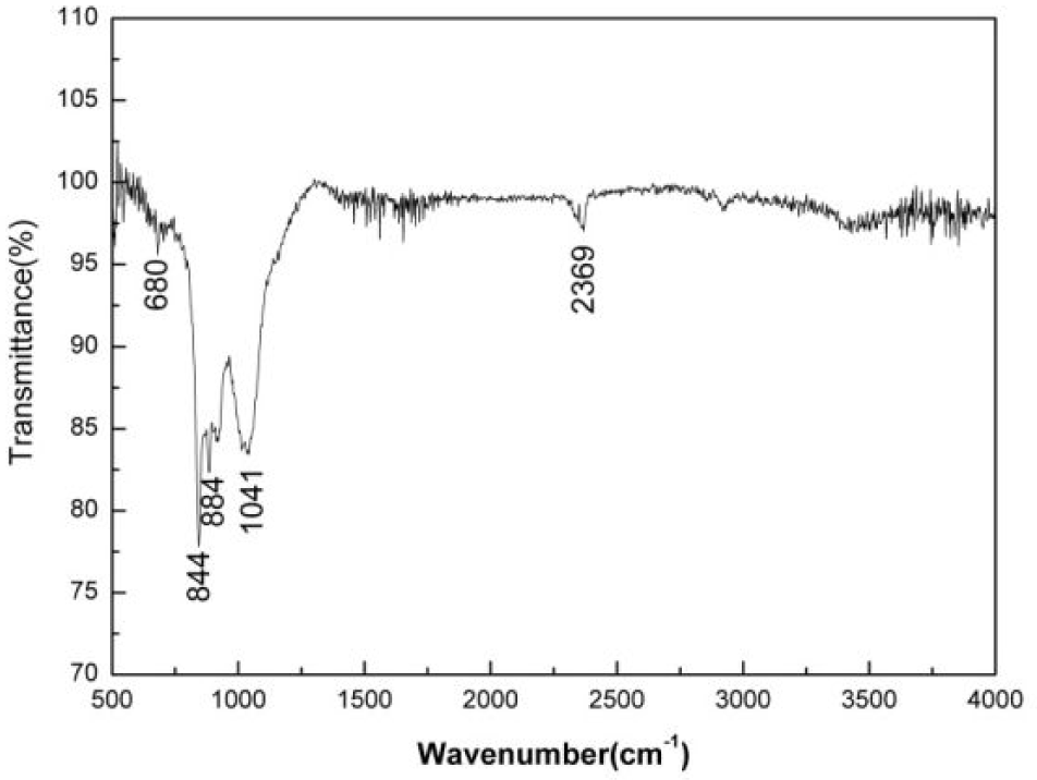
FTIR spectrum of Si3N4 nanowires synthesized by nitridation of SiO at 1500°C
The microcosmic morphologies of the Si3N4 nanowires were observed by SEM. Figures 3 (a-b) show that the obtained nanowires possessed a cylindrical structure with a smooth surface and a diameter of nearly 80∼250 nm. As Figure 3c shows, most of the nanowires grew to a diameter of about 200 nm, while there were several bold nanowires with a diameter of 500 nm. No droplets were found on the tip of the nanowires. Figure 3d shows that large quantities of aligned nanowires grew homogeneous on the surface of the Al2O3 plate and attained a length of several hundred micrometres. The bending morphologies of several nanowires also suggest a superior flexural strength.

(a) SEM of single Si3N4 nanowires with smooth surface; (b) SEM of Si3N4 nanowires with a diameter of nearly 80∼250 nm; (c) SEM of several Si3N4 nanowires without droplets; (d) SEM of aligned Si3N4 nanowires grown on the alumina substrate
Further characterization of the synthesized nanowires was completed using HRTEM. As Figure 4a shows, the nanowires possessed a diameter of 80 nm and 190 nm. The fragments scattering around the nanowires were caused by the grinding of products during sample preparation. The crystal structure is given by Figure 4b. The spacing distances between two adjacent fringes in different planes had an equal value of 0.672 nm, which was consistent with the distance of [100] planes of the hexagonal crystal lattice of α-Si3N4 with a space group of P31c(159). The spacing between lattice planes, as well as atom distribution also indicated a preferred growth direction of [100,23–24]. The surfaces of the nanowires were sometimes coated with thin amorphous layers. This can often be observed in many synthesized Si3N4 nanowires [25].
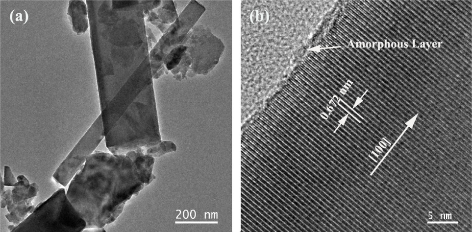
(a) TEM image of the α-Si3N4 nanowires surrounded by scattered fragments; (b) TEM and FFT image of the α-Si3N4 nanowires with a spacing distance of 0.672 nm and a growth direction of [100], corresponding to hexagonal α-Si3N4
To further investigate the surface states of the Si3N4 nanowires, depth profile by XPS was conducted with different etch times; element messages with different depths are also shown in Figure 1 and Table 1. The results revealed that the surface of the Si3N4 nanowires contained a Si element, N element, O element and a C element. The C element and part of the O element were derived from common contamination impurities inherent in XPS tests. Regardless of this, the variation trend among elements could still be observed via the XPS spectrum of the typical Si3N4 nanowires. With an increase in etch level, the content of the Si element and N element increased correspondingly. Meanwhile, the content of the C element and O element sharply decreased. This result notes the gradual change of elements in the amorphous layers of the Si3N4 nanowires, as shown in the TEM image.
Mole per cent and peak position of Si, N and O at different etch levels

The XPS spectrum of the Si element was also investigated. The peak positions of Si2p were found to be in the surface shift between 101.78 eV and 102.48 eV. The binding energy scale of Si2p in monatomic Si is 97.7–99.2 eV. Here, we can infer that there was no monatomic Si in the surface of Si3N4 nanowires, because there was no peak position lower than 100 eV. The O element, except for the impurity in the test, was primarily derived from SiOx (peak position at Si2p: 102 eV). Meanwhile, the peak position of the O element in SiOx also corresponded to Table 1, which can be assumed as evidence for the existence of SiOx. The O element in the surface of nanowires may have been derived from the impurity of the N2 and the growth process.
The resistance of the Si3N4 nanowires to oxidation at high temperatures was evaluated by TG-DSC in air. As Figure 5 shows, the weight of the nanowires remained steady at a relatively low temperature and rose sharply when at temperatures above 1135 °C. Two exothermic peaks emerged in the position of 1210°C and 1290°C. This may correlate with the two reactions presented below:

XPS spectrum of the typical Si3N4 nanowires and Si element

TG-DSC data of Si3N4 nanowires in air at temperatures ranging from 100°C to 1500°C.


Compared to the bulk of Si3N4 materials, Si3N4 nanowires showed poor performance regarding oxidation resistance. The oxidation resistance ability of Si3N4 ceramics ultimately rests on the integrity and stability of the surface oxide layer [26]. Considering their special morphology and limited diameter, the Si3N4 nanowires find it difficult to form an integrated surface oxide layer prior to absolute oxidation. Their limited diameter also leads to forming a large specific surface area and high surface energy. Hence, Si3N4 nanowires react with oxide more easily than bulk Si3N4.
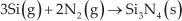
For the growth process, vapour phase growth was extensively used for producing nanowires; additionally, several models, including vapour-solid (VS) and vapour-liquid-solid (VLS) mechanisms were proposed to explain the growth mechanism for crystalline nanowires [27]. Compared to the VS mechanism, the VLS mechanism possesses three growth stages: metal alloying, crystal nucleation and axial growth [28], resulting in the catalyst ball on the end of nanowire as a special morphological feature. Considering that no droplets were found on the end of nanowires and no metal catalyst was added, we prefer the VS mechanism for the growth process. This process includes three steps: evaporation, gaseous reaction and nucleation. With a rise in temperature, the SiO thermally decomposes to Si and SiO2, and can be shown as follows:

The Si phase in the residual materials can also be formed in this way. As for the Si2N2O and SiC, these can be formed by the reaction of Si and SiO2 with N2 and the carbon on the graphite crucible with high activity.
Then, the vapour phase of Si reacts with N2 as follow:
The newly generated Si3N4 then condenses and acts as the source for the original nucleus. Large quantities of nuclei are formed on the surface of the Al2O3 plate and lead to a high yield of nanowires. With the consistent transport of the vapour phase of Si to the surface of the nucleuses, the crystal Si3N4 grows as an epitaxial in the direction of the lowest energy found in crystallography, which was found to be [100]. Finally, the Si3N4 nanowires continue to grow via this typical VS process.
Since the vapour phase of Si is directly generated from the decomposition of raw materials, the density of the vapour phase can be high and as a result lead to inhomogeneous nanowires. For this research, we diluted the Si vapour by means of flowing N2 and placed the Al2O3 plate in a position away from the raw materials. The results show that the nanowires grew homogeneously on the Al2O3 plate. Meanwhile, a high flow rate of N2 will reduce the growth of nanowires [29]. Hence, it is important to control the flow rate of the N2.
4. Conclusions
In summary, Si3N4 nanowires were successfully synthesized using an Al2O3 plate as substrate and SiO as silicon source. Nanowires with an average diameter of 200 nm consisted primarily of α-Si3N4 and grew in the direction of [100] to a length of several hundred micrometres. Si3N4 nanowires will be significantly oxidized in air at a temperature above 1135°C. The growth process of the nanowires was inferred to be a VS mechanism. The proper flow rate is also essential for the yield and quality of nanowires. Considering the easy procedures and high yield, this method can be a good choice for the high yield of Si3N4 nanowires. The evaluation of oxidation resistance ability and the element message of the surface of the nanowires may also offer references to the application of Si3N4 nanowires.
Footnotes
5. Acknowledgements
The financial support of the National Science Foundation of China (No. 50902150), Aid Program for Science and Technology Innovation Research Team in Higher Educational Institution of Hunan Province, Aid Program for Innovative Group of National University of Defense Technology are all gratefully acknowledged.