
Abstract
The matrix-dependent strain distributions of Au and Ag nanoparticles in a metal-oxide-semiconductor based nonvolatile memory device are investigated by finite element calculations. The simulation results clearly indicate that both Au and Ag nanoparticles incur compressive strain by high-k Al2O3 and conventional SiO2 dielectrics. The strain distribution of nanoparticles is closely related to the surrounding matrix. Nanoparticles embedded in different matrices experience different compressive stresses, which provide opportunities for tailoring the microstructure of Au and Ag nanoparticles. This opens up ways for exploring strain effects on physical properties and further tunes the charge storage properties of nanoparticles.
Keywords
1. Introduction
Recently, nonvolatile memory (NVM) devices, with nanoparticles as their memory element, have attracted significant attention in terms of their data storage applications. Compared to traditional floating gate memory, a structure with nanoparticles embedded in the dielectrics exhibits high potential for producing memory with low operating voltage, high endurance, fast write-erase speeds and better immunity to soft errors [1-3]. Research regarding memory-cell structure that employs metal nanoparticles has been studied in recent years, especially studies that include Au and Ag nanoparticles. In recent work, we found that Au and Ag nanoparticles possessed good charge storage properties [4, 5]. In addition, the use of high-k dielectrics rather than conventional SiO2 has brought significant improvements to nanoparticle-based memory devices in terms of programming efficiency and data retention [4, 5]. Al2O3 with a dielectric constant (∼9) more than twice that of SiO2 (∼3.9) is a promising candidate for serving as a gate dielectric [5].
Moreover, recent studies have found that the charge storage capabilities of nanoparticle-based memory devices are associated with the defect states of the surface of the nanoparticles. These defect states can capture charge and serve as charge storage centres, and can result in enhanced charge storage properties [6-8]. Recently, it was demonstrated that the growth of nanoparticles embedded in a host matrix can lead to substantial strain [9-11]. This strain can be relaxed via the growth process of nanoparticles and subsequently produce many defects at the nanoparticle/matrix interface, thus influencing the physical properties of nanoparticles [12]. Meanwhile, the strain experienced by the nanoparticles is closely related to the surrounding matrix, which will have a different impact on the physical and chemical properties of the nanoparticles [13, 14]. Moreover, recently, it was demonstrated that the defects associated with strained nanoparticle interfaces can capture charges and serve as charge storage centres, leading to improvements in charge storage performance [3]. Therefore, in order to better understand the charge storage properties of Au and Ag nanoparticles, the strain distribution of the Au and Ag nanoparticles embedded in a high-k Al2O3 and conventional SiO2 dielectric is investigated in this study. The matrix-dependent strain provides an opportunity for engineering the charge storage properties of the nanoparticles.
2. Simulation
Recently, a simple approach was developed for the formation of Au and Ag nanoparticles embedded in a solid state matrix through modification of the pulsed laser deposition (PLD) technique [4, 5]. In order to investigate the tuning effect on the strain as the result of the morphology of embedded Au and Ag nanoparticles, a finite element (FE) simulation was performed to simulate the strain distribution of embedded Au and Ag nanoparticles. The FE calculation is a versatile computer simulation technique used for continuum modelling of deformation in materials [15]. The simulations are conducted to account for the physical properties of many materials, including elastic anisotropy, thermal expansion and three-dimensional object shape, among others [16-18]. Figure 1 presents a schematic view of metal-oxide-semiconductor (MOS) capacitor structure with metal nanoparticles embedded in the dielectric. In our FE model, we set two types of nanoparticle sizes. For nanoparticles with a size of 2.5 nm, the thicknesses of blocking and tunnelling oxide layers were roughly 10 and 5 nm, respectively. For nanoparticles with a size of 3.5 nm, the thicknesses of blocking and tunnelling oxide layers were roughly 9.5 and 4.5 nm, respectively. We used the Al2O3 and the SiO2 as blocking and tunnelling oxide layers in the tri-layer memory structure, respectively. We also used Au or Ag as metal nanoparticles, respectively. Au or Ag nanoparticles embedded in the dielectrics could clearly be seen between the tunnel oxide and the blocking oxide.

Schematic view of metal nanoparticles embedded in the dielectrics
In general, the nanoparticle formation mechanism can be explained as follows: the probability for nucleation increases at higher temperatures; thus, the density of nanoparticles is higher. Once sufficient surface energy is available, the number of nanoparticles increases rapidly as fresh nuclei is formed, while the nanoparticles already formed by nucleation continue to grow by adatom attachment via surface diffusion, leading to agglomeration of bigger nanoparticles alongside increasing temperature. Due to the thermal expansion mismatch, the formation of nanoparticles in a matrix may be accompanied by the generation of compressive strain. During the growth process, the matrix exerts a compressive strain on Au and Ag nanoparticles, due to the volume expansion of the Au and Ag nanoparticles. In order to clarify strain influences, the strain distributions of Au and Ag nanoparticles were qualitatively simulated by FE calculations, which were performed using the commercial software package ANSYS [3]. In the simulation, the FE model for the strain generation was based on the following assumptions: the strained state of a nanoparticle can be regarded as resulting from the insertion of a nonstrained particle, of some volume Vp, into a cavity of volume Vc within a nonstrained matrix. The stress P is caused by the volume misfit Vp – Vc and has, in the case of spherical particle and cavity shape, the following value [19]:

where Kp and G are the compression modulus of the particle and the shear modulus of the matrix, respectively. The strained state of the particle results from a gradual volume contraction, from Vp down to the actual volume V of the stressed particle, when the stress increases from zero to P. Strain distributions can be generated by the thermal expansion mismatch, because of the growth of Au and Ag nanoparticles. As the size of nanoparticles and the thickness of the thin film are of the same order of magnitude, in the FE calculation, the Al2O3 and the SiO2 matrix are considered to be infinite in the side and bottom directions of the Au or Ag nanoparticles, while the Al2O3 and the SiO2 matrix are finite in the top direction of Au or Ag nanoparticles. Therefore, in our model, fixed displacement boundary conditions were imposed at the lateral side and the bottom surface of matrix, while the top surface of matrix was allowed to expand freely. Young's modulus was taken to be 170, 76, 360 and 55.6 GPa for Au, Ag, Al2O3 and SiO2, respectively. Poisson's ratio was taken to be 0.42, 0.38, 0.24 and 0.16 for Au, Ag, Al2O3 and SiO2, respectively.
3. Results and Discussion
Figure 2 (a) and (b) show the cross-sectional strain distributions of Au and Ag nanoparticles with a size of 2.5nm embedded in a high-k Al2O3 matrix, respectively; (c) and (d) show the cross-sectional strain distributions of Au and Ag nanoparticles with a size of 3.5nm embedded in a high-k Al2O3 matrix, respectively. The strain distribution is distinguished by different colours, as indicated by the marks in Figure 2. Correspondingly, Figure 3 (a) and (b) show the X-Y plane strain profiles of Au and Ag nanoparticles with a size of 2.5nm embedded in a high-k Al2O3 matrix, respectively; (c) and (d) show the X-Y plane strain profiles of Au and Ag nanoparticles with a size of 3.5nm embedded in a high-k Al2O3 matrix, respectively. Figure 2 (a)-(d) and Figure 3 (a) -(d)indicate that the strain distribution of the Au and Ag nanoparticles grown in the Al2O3 matrix is inhomogeneous. It can also be seen that the strain at the centre of the Au and Ag nanoparticles is distributed homogeneously and the compressive strain at the centre of Au nanoparticles is much weaker than that at the centre of Ag nanoparticles. Moreover, for the Au and Ag nanoparticles, the strain existing at the surface of the nanoparticles is weaker than that at the centre of the nanoparticles. Additionally, the entire strain of the metal nanoparticles becomes larger with an increase in the size of the metal nanoparticles.
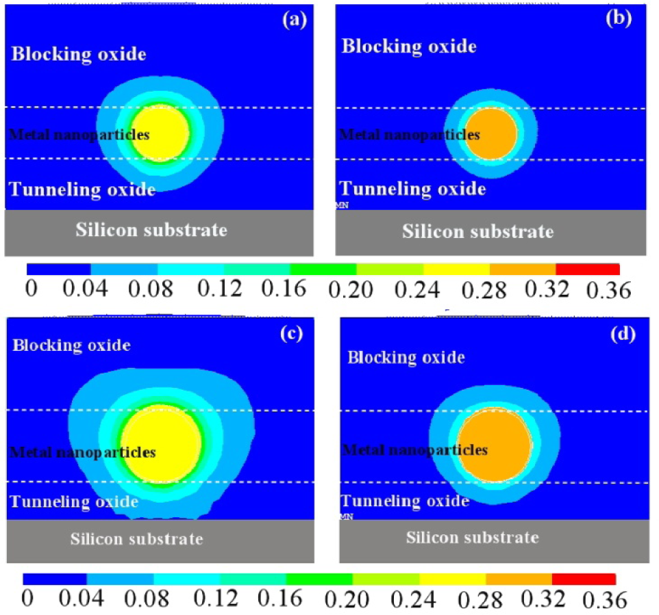
(a) and (b): cross-sectional strain distribution of Au and Ag nanoparticles with a size of 2.5nm embedded in the high-k Al2O3 matrix, respectively; (c) and (d): cross-sectional strain distribution of Au and Ag nanoparticles with a size of 3.5nm embedded in the high-k Al2O3 matrix, respectively

(a) and (b): X-Y plane strain profile of Au and Ag nanoparticles with a size of 2.5nm embedded in the high-k Al2O3 matrix, respectively; (c) and (d): X-Y plane strain profile of Au and Ag nanoparticles with a size of 3.5nm embedded in the high-k Al2O3 matrix, respectively
Figure 4 (a) and (b) show the cross-sectional strain distributions of Au and Ag nanoparticles with a size of 2.5nm embedded in the conventional SiO2 matrix, under the same conditions as in Figure 2, respectively; (c) and (d) show the cross-sectional strain distributions of Au and Ag nanoparticles with a size of 3.5nm embedded in the conventional SiO2 matrix, respectively. Correspondingly, Figure 5 (a) and (b) show the X-Y plane strain profiles of Au and Ag nanoparticles with a size of 2.5nm embedded in the conventional SiO2 matrix, respectively; (c) and (d) show the X-Y plane strain profiles of Au and Ag nanoparticles with a size of 3.5nm embedded in the conventional SiO2 matrix, respectively. It can be seen that both the Au and Ag nanoparticles incur compressive strain from the SiO2 matrix. The strain distribution of the Au and Ag nanoparticles grown in the conventional SiO2 matrix is also inhomogeneous. Furthermore, the strain existing at the centre of the Au and Ag nanoparticles and exerted by SiO2 is homogeneously distributed; the compressive strain existing at the centre of Au nanoparticles is much weaker than that at the centre of Ag nanoparticles. Moreover, for the Au and Ag nanoparticles, the strain existing at the surface of the nanoparticles is stronger than that at the centre of the nanoparticles. Additionally, the entire strain of the metal nanoparticles becomes larger with an increase in the size of the metal nanoparticles.

(a) and (b): cross-sectional strain distribution of Au and Ag nanoparticles with a size of 2.5nm embedded in the conventional SiO2 matrix, respectively; (c) and (d): cross-sectional strain distribution of Au and Ag nanoparticles with a size of 3.5nm embedded in the conventional SiO2 matrix, respectively

(a) and (b): X-Y plane strain profile of Au and Ag nanoparticles with a radius size of 2.5nm embedded in the conventional SiO2 matrix, respectively; (c) and (d): plane strain profile of Au and Ag nanoparticles with a radius size of 3.5nm embedded in the conventional SiO2 matrix, respectively
Figures 2-5 show that strain distribution strongly depends on the host matrix. It should be noted that the compressive strain that exists on the Au or Ag nanoparticles embedded in the Al2O3 matrix is much stronger than on those embedded in the SiO2 matrix. Moreover, for the Au or Ag nanoparticles embedded in the Al2O3 matrix, the compressive strain existing in the centre nanoparticle is stronger than that at the surface of the nanoparticle. Contrarily, for the Au or Ag nanoparticle embedded in SiO2 matrix, the compressive strain existing in the centre of nanoparticles is weaker than that at the surface of nanoparticles. According to our simulation process, these phenomena can be attributed to the fact that Young's modulus of Au is larger than that of Ag and Young's modulus for both Au and Ag is larger than that of SiO2, but smaller than that of Al2O3. Recently, Campera et al. [20] modelled the experimental data of De Salvo et al. [21] and concluded that electrons are stored in defects in the nanocrystals/oxide interface. Our previous research has also demonstrated that the defects associated with the strained GaAs nanoparticles interfaces can capture charges and serve as charge storage centres, causing improvement in charge storage performance [3]. Compressive strain is imposed on the interface of Au and Ag nanoparticles and the surrounding matrix, which contains a large fraction of the constituent atoms, leading to the formation of strain-relaxing defects at the surface of nanoparticles [22]. Moreover, due to the stronger strain experienced by the nanoparticles, significantly more strain-relaxing defects will be generated at the surface of nanoparticles [12]. The defects can capture charges and serve as charge storage centres, causing improvement in charge storage performance. Figure 6 (a) and (b) show the strain intensities of the surface of Au and Ag nanoparticles with a size of 2.5nm and 3.5nm embedded in the Al2O3 and SiO2 matrix, respectively. It can be seen that the compressive strain existing at the surface of the Au nanoparticle is stronger than that at the surface of the Ag nanoparticle in both the Al2O3 and SiO2 matrices. This phenomenon can be attributed to the fact that Young's modulus of Au is larger than that of Ag. Therefore, from our simulation, the compressive strain existing at the surface of the Au nanoparticles with a size of 3.5nm embedded in the SiO2 matrix is strongest, which can lead to the formation of significant strain-relaxing defects at the surface of the nanoparticles, leading to the best charge storage performance. The matrix-dependent strain provides an opportunity for engineering the charge storage properties of nanoparticles. This suggests that the compressive strain applied on the nanoparticles has a significant influence on the charge storage properties of the memory devices.
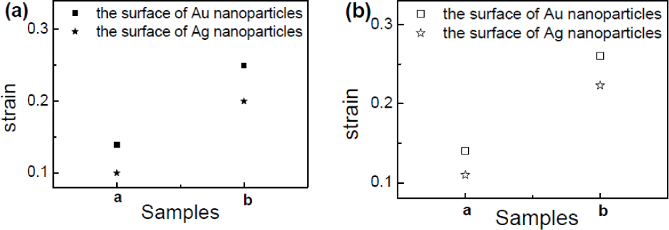
(a): strain intensities of the surface of the Au and Ag nanoparticles with a size of 2.5nm embedded in the Al2O3 (sample a) and SiO2 (sample b); (b) strain intensities of the surface of the Au and Ag nanoparticles with a size of 3.5nm embedded in the Al2O3 (sample a) and SiO2 (sample b)
4. Conclusions
In summary, the matrix-dependent strain distributions of Au and Ag nanoparticles in a metal-oxide-semiconductor-based nonvolatile memory device were investigated through the use of finite element calculations. The interplay between Young's modulus of a matrix and a nanoparticle was shown to play a significant role regarding the nanoparticle. We demonstrated that nanoparticles embedded in different matrices experience different compressive stresses. The charge traps associated with the strained Au and Ag nanoparticles interfaces can manipulate the charge storage properties of Au and Ag nanoparticles embedded in high-k dielectric materials. The matrix-dependent strain provides an opportunity for engineering the charge storage properties of the nanoparticles and provides the potential for an exciting combination of fundamental science with a potentially wide array of applications such as high-density information storage devices.
Footnotes
5. Acknowledgements
This work was supported by the Natural Science Foundation of China (Grant No.: 51461019, 11164008, 51561012 and 51361013), the Project for Young Scientist Training of Jiangxi Province (Grant No.: 20153BCB23016), the Natural Science Foundation of Jiangxi Province (Grant No.: 20151BAB202004) and the research fund of Jiangxi Normal University (Grant No.: 6628).