
Abstract
A reminder, a review and a look toward the future prospects for quantum dot-sensitized solar cells — a reminder of the highly viable, energy-efficient solar cells achievable; a review of ground-breaking devices and their similarities to the near unity photon-to-electron mechanisms of photosynthesis; a look toward architectures that capitalize on the advances observed in previous work.
1. Introduction
With the surge of silicon solar cells from China driving the cost of solar cells to all-time lows, the economic benefit of the quantum dot-sensitized solar cell is falling under scrutiny. However, while the financial benefits of the inexpensive materials used to fabricate quantum dot-sensitized solar cells have been expounded as an advantage, the need for and long-term benefits of quantum dot-sensitized solar cells extend beyond economic considerations. A review of the environmental benefits and potential of quantum dot-sensitized solar cells, a brief summary of some key progressive devices and an overview of our approach towards an optimal quantum dot-sensitized solar cell are contained within this manuscript to serve as a reminder of the hopes raised when quantum dot-sensitized solar cells were first introduced [1,2] and the environmentally friendly and economically efficient products that are still achievable if the correct device architecture can be obtained.
To fully understand the environmental benefits of quantum dot-sensitized solar cells, an assessment of the negative impact and costs of silicon solar cell fabrication must be considered. Silicon is the most common element after oxygen within the earth's crust, so utilization of such a readily available material seems ideal. However, harvested silicon is not viable for use in solar cells unless it is processed. It must undergo Siemens purification to reach a level of purity conducive to efficient energy production and collection [3]. Siemens purification is a minimum of 18 high-energy input steps, whose by-products are hazardous chemicals such as hydrochloric acid. In fact, the purification process consumes so much energy, the Hemlock Semiconductor Group (Hemlock, MI), which purifies silicon for use in solar cells and electronics, reported in 2013 that at 420 MWs its energy-usage was the highest for any single-site energy consumer in Michigan [4]. This energy requirement is for the operation of the purification plant only; it does not include the energy required to fabricate the actual solar cells.
In addition to costly initial purification of the solar cell materials, silicon solar cells have a limited photoactive region and energy collection capability. Bulk silicon has an indirect bandgap of 1.1 eV, which limits its ability to effectively harness the energy of the solar spectrum. In addition to the bandgap energy limitation, the molar extinction coefficient for silicon at the bandgap [5] is 1.30 × 10⁻⁵ eV, which means that of photons that exceed the bandgap only a very small portion are absorbed within the path length of the silicon devices. Beyond the physical limitations of silicon, utilization of it within a bulk p-n junction places a thermodynamic limit on energy efficiency of about 30%, commonly referred to as the Shockley-Queisser limit [6]. Some progress has been made in overcoming these limitations by utilizing micro-patterned Si as artificial photosynthesis systems [7,8], sliver cells, polycrystalline devices and solar energy concentrators; large-scale production of Si solar cells still relies on purified precursors assembled into bulk heterojunctions.
Like many other aspects of science, nature provides a prominent example of an ideal system. Nature, through billions of years of evolutionary trials, has created the reaction centres and molecular wiring necessary to produce a 99% photon-to-electron production efficiency during photosynthesis [9]. For simplicity, we will follow the photosynthetic pathway of photosystem I. In photosystem I, photoexcited electrons within membrane-bound chlorophyll are transferred along their energy gradient to the P700 reaction centre through two core chlorophyll. The electrons flow through an internal electron chain to pheophytin then to quinone, where they are transferred to a terminal iron-sulphur complex. The electrons are collected by ferredoxin for use in further photosynthetic reactions. The “vacant” hole is scavenged by soluble plastocyanin [10]. Photosynthesis owes its high quantum efficiency to two core concepts: 1. Rapid transport of the photoexcited electron wherein extraction across the thylakoid membrane occurs in less than 1 μs [10], and 2. Physical and energetic separation of the charge carriers. An ideal solar cell architecture would capitalize on these concepts while also containing readily accessible, low energy-input materials. For mankind to fully achieve an energetically efficient solar cell, a device architecture mimicking nature's integrated system of molecular engineering, effective light harvesting and charge extraction is needed. Quantum dot-sensitized solar cells, which emulate the architecture proposed by Grätzel in 1991 for dye-sensitized solar cells [11], meet the above requirements. To provide a visual comparison of charge generation and migration within quantum dot-sensitized solar cell and during photosynthesis, Figure 1 depicts a simplified version of a quantum dot-sensitized solar cell beside the P700 reaction centre of photosystem I. The similarities of the two systems are readily apparent with a light-harvesting unit (chlorophyll or quantum dot) becoming excited by light to generate an electron-hole pair which is separated and each carrier is transferred through different media (either across a thylakoid membrane or within nanoparticle network) along the energetic gradient of the charge-carriers. However, the electron-transfer rate in photosystem I is 47 e−/s [12] which is minimal compared to the electron-transfer rate between quantum dots and TiO2, which is reported to be between 107 and 1010 e−/s depending on the binding environment of the quantum dots [13-16].

Comparison of charge generation and migration during photosynthesis in the P700 reaction centre of photosystem I and during photoexcitation in a quantum dot, which acts as an artificial reaction centre in a quantum dot-sensitized solar cell (QDSSC)
In addition to the above similarities of the entire quantum dot-sensitized solar cell to photosystem I, quantum dots act as an artificial reaction centre, separating the electron and hole on the femtosecond timescale [17,18] with the carriers moving along the energetic gradient created by the inherent dipole of the quantum dot [19] due to top and bottom terminating planes of cations or anions [20]. Also, photosystem I agents like quantum dots rely on quantum mechanics and nanostructuring to optimize energy collection [21].
Since the introduction of the Grätzel dye-sensitized solar cell [11] and its closely related derivative the quantum dot-sensitized solar cell [2], a great deal of research has been conducted to utilize and improve the tremendously advantageous combination of readily available materials and efficient charge extraction through energetic separation of charge carriers. Efforts have focused on overcoming some of the limitations of the original Grätzel cell design such as limited active layer volume, less than optimal energy harvesting and carrier recombination. Two well-investigated options are replacing the TiO2 nanoparticle network with vertically aligned nanotubes [23-33] and exchanging the light-harvesting dyes with quantum dots [22,34–35]. The nanotubes increase the active layer volume by increasing the specific surface area that can be functionalized by the light harvesters and have the added benefit of increasing electron lifetime within the TiO2 by up to three orders of magnitude [36]. Also, the commonly employed Ru-based dyes (N3 and N719) [37] absorb the same portion of the solar spectrum as certain quantum dots; however, quantum dots do so more effectively with size-dependent molar extinction coefficients several orders of magnitude larger than the organic dyes [38]. Another benefit of using quantum dots is the possibility of generating multiple excitons from a single photon [39-43], which under appropriate conditions allows for higher than unity quantum efficiency.
Another common issue associated with the Grätzel cell is leakage of the liquid electrolyte which can cause efficiency loss and be a potential health hazard (iodide/triiodide electrolytes have an acute toxicity rating of four, and are known irritants to skin, eyes and mucous membranes) [44]. Hodes published an in-depth comparison of the recombination types and rates observed in dye-sensitized and semiconductor-sensitized solar cells [45], in which he reports that within a system with a solid hole-conducting material the hole-injection rate from the light-harvester is six orders of magnitude faster than electron injection from the TiO2. While the exact ratio would be dependent on the specific system, solid hole-conductors seem to disfavour carrier recombination more than a liquid electrolyte system. Early research to replace the liquid electrolyte explored replacing it with conductive, organic polymers [46-49]; more recently the use of inorganic semiconductors as possible alternatives has emerged [50-57].
One approach would be to remove the liquid electrolyte and fill the interim with solid indium-tin oxide, which — just as in the original Grätzel cell — is energetically resonant with the hole [9,11]. In our nanostructured, solid-state device (Figure 2), PbS quantum dots absorb photons, generating an electron-hole pair. The photo-generated electron, travelling down its energy gradient, is injected into a TiO2 nanotube, where it travels out of the device into the Ti foil contact. The photo-generated hole, following a path similar to those discussed by Gao et al. for hole conduction in n-type metal oxides [58], transfers into indium-tin oxide via shallow gap states. The device is analogous to the Grätzel cell with the critical difference being that the device separates charge generation and migration by utilizing a unique combination of inorganic solid materials, which removes sealing and leakage issues associated with liquid electrolytes and should reduce carrier recombination.

Nanostructured, solid-state photovoltaic device design: PbS quantum dots form a layer at the interface between TiO2 nanotubes and indium-tin oxide. Upon excitation of the quantum dots, photoexcited electrons inject into nanotubes and the holes transfer into the indium-tin oxide to be carried to an external circuit to perform work.

Schematic of hydrogen peroxide pre-treatment and anodization of titanium foil to produce TiO2 nanotubes

Schematic of successive ion layer adsorption and reaction for in situ deposition of PbS quantum dots into TiO2 nanotubes
The device is fabricated by anodizing a Ti foil to generate TiO2 nanotubes, which are subsequently functionalized with PbS quantum dots and filled with indium-tin oxide. To fully exploit the surface area available and prevent carrier recombination, both the interior and exterior walls of the nanotubes need to be covered with a monolayer of quantum dots. While multiple layers of quantum dots would increase light harvesting, indirect carrier recombination between quantum dots would reduce the overall efficiency [45]. Once the nanotubes are functionalized with the light-harvesting quantum dots, indium-tin oxide must fill all of the interim space to prevent charging of the quantum dots leading to device instability and degradation. To discern the optimal quantum dot-functionalization method, three different deposition techniques (successive ion layer adsorption and reaction, electrophoretic and chemical linking) were investigated. Indium-tin oxide was deposited using either electrochemically assisted deposition or electron beam evaporation to find the best conformal filling with minimal impact on the quantum dots.
2. Experimental Procedure
2.1 Nanotube Fabrication
Fabrication of the TiO2 nanotube array follows a slightly modified version of the commonly employed anodic oxidation of a Ti foil. In short, a Ti foil (purchased from Sigma-Aldrich at 97% purity and cut into 1″×1″ squares using a machine press) was pre-treated by soaking in an 80°C hydrogen peroxide solution for three days, followed by soaking in 1M hydrochloric acid for one hour [59]. After pre-treatment, the foil was anodized at 40 V for two hours in a two-electrode electrochemical cell with a Pt mesh counter electrode, 0.3% ammonium fluoride and 2% water in ethylene glycol electrolyte [23-33]. The pre-treated foil when anodized yielded nanotube arrays with wider pores and less surface debris than untreated foils.
2.2 Quantum Dot Deposition
2.2.1 Successive Ion Layer Adsorption and Reaction: In Situ Synthesis of Quantum Dots
Successive ion layer adsorption and reaction is a relatively simple process in which the nanotube array was soaked for one minute in 1mM lead acetate solution in methanol, rinsed with methanol, soaked in 1mM sodium sulphide solution in methanol for one minute and then rinsed again [32,60]. Lead cations that adsorbed to the surface of the nanotubes during the first step are reacted with sulphur anions in the third step to nucleate PbS quantum dots. The entire process was repeated for a total of five cycles to ensure quantum dot nucleation and growth.
2.2.2 Electrophoretic Deposition of Colloidal Quantum Dots
Electrophoretic deposition and chemical linking are significantly different from successive ion layer adsorption and reaction in that they utilize pre-synthesized, colloidal PbS quantum dots. The colloidal quantum dots were synthesized through a solvothermal reaction of lead oleate and hexamethyldisilathiane; the synthesis of which is detailed in previous literature [39]. For electrophoretic deposition, the nanotube array and a Pt mesh counter electrode (separation = 0.5 cm) were submerged in an optically dilute (O.D. = 0.05 a.u.) solution of PbS quantum dots in hexanes [61–62]. A potential bias of 200 V was applied between the electrodes for 20 minutes. The electric field between the electrodes induced quantum dot migration and adhesion to both of the electrodes.

Schematic of electrophoretic deposition of colloidal PbS quantum dots into TiO2 nanotubes
2.2.3 Chemical Linking of Colloidal Quantum Dots
Chemical linking, which also utilizes pre-synthesized PbS quantum dots, uses a bifunctional ligand (1,3-mercaptopropionic acid, in this case) to create a direct link between the surface of the nanotubes and the quantum dots [63-65]. The nanotube array was soaked in a 10% mercaptopropionic acid in methanol solution for 24 hours. The carboxylic acid group of mercaptopropionic acid linked to the surface of the nanotubes during this time. The array was rinsed with methanol and transferred to an optically dilute (O.D. = 0.05 a.u.) solution of PbS quantum dots in hexanes, where it soaked for another 24 hours. The thiol group of the mercaptopropionic acid linked to the quantum dots during this time. The array was rinsed with methanol and allowed to air dry.

Schematic of chemical linking of colloidal PbS quantum dots to TiO2 nanotubes using mercaptopropionic acid (MPA)
2.3 Indium-Tin Oxide Deposition
2.3.1 Electrochemically Assisted Deposition of Indium-Tin Oxide
For electrochemically assisted deposition, the nanotube array sensitized with quantum dots, a Pt mesh counter electrode and an Ag/AgCl reference electrode were submerged in an 80°C solution of 10 mM In(NO3)3, 1 M KNO3, 4.6 mM HNO3 and 1 mM SnCl4, similar to the conditions used to produce indium-tin oxide nanowires inside gold-plugged nanotubes [66,67]. Following the synthetic scheme described by Kovtyukhova and Mallouk to produce the indium-tin oxide nanowires, an optimal reduction potential of −0.8 V (determined by linear sweep voltammetry on a Ti foil in 1 M KNO3) was applied to generate a localized pH increase by reducing nitrate and dissolved oxygen, causing indium-tin hydroxide complexes to precipitate out of the solution into the nanotube array. Subsequent annealing at 450°C converts the hydroxide complexes into indium-tin oxide. After annealing, the deposition and crystallinity of the indium-tin oxide was confirmed using glancing angle x-ray diffraction.
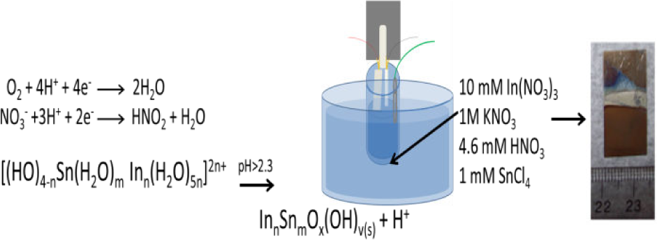
Schematic of electrochemically assisted deposition of indium-tin oxide into PbS quantum dot-sensitized TiO2 nanotubes
2.3.2 Electron Beam Evaporation and Deposition (Electron Beam Evaporation) of Indium-Tin Oxide
For electron beam evaporation of indium-tin oxide, an Ångstrom Åmod e-beam chamber (Ångstrom Engineering; Kitchener, ON) was utilized. An indium-tin oxide target composed of 90% indium oxide doped with 10% tin oxide was evaporated using a steady state power of ∼210 kW to maintain a deposition rate of 0.5 Å/s. To crystallize the oxides, devices were annealed in a tube furnace in air at 450°C for three hours. The heating and cooling ramp periods were also three hours. The deposition and crystallinity of the indium-tin oxide was confirmed using glancing angle x-ray diffraction on devices post-annealing.

Schematic of electron beam evaporation and deposition of indium-tin oxide into PbS quantum dot-sensitized TiO2 nanotubes
3. Results and Discussion
Figure 9 provides a map of each step of device fabrication and the pertinent results determined to impact device performance relating to that step. While our current experimental findings do not merit praise as state-of-the-art, the results are provided in compilation with other literature findings so that this article may act as a guide for creating state-of-the-art quantum dot-sensitized solar cells.

Illustrative map of device production and pertinent results of each step of device fabrication
3.1 Quantum Dot Quality and Infiltration
A difficulty associated with working with nanotubes fabricated on a Ti substrate when depositing quantum dots from solution is overcoming surface tension effects, which tend to inhibit the solution from completely filling the pores. To confirm that infiltration occurred with the deposition techniques used, scanning electron microscopy coupled with energy dispersive x-ray spectroscopy of side-profiles of quantum dot-functionalized TiO2 nanotubes were obtained. As observable in Figure 10, all profiles exhibit Pb and S signals along the length of the nanotubes, indicating infiltration of the quantum dots. The absorbance spectra of pre-synthesized colloidal PbS quantum dots and successive ion layer adsorption and reaction synthesized quantum dots on nanotubes, grown on a transparent conductive oxide on glass to allow transmittance of the light, are shown in Figure 11. For the pre-synthesized colloidal quantum dots used for electrophoretic deposition and chemical linking, a single narrow absorption peak is observed at λmax= 1170 nm. For the successive ion layer adsorption and reaction synthesized quantum dots the broadness of the peak at λmax1= 1162 nm is indicative of the polydispersity that is further confirmed by transmission electron microscopy in Figure 12.
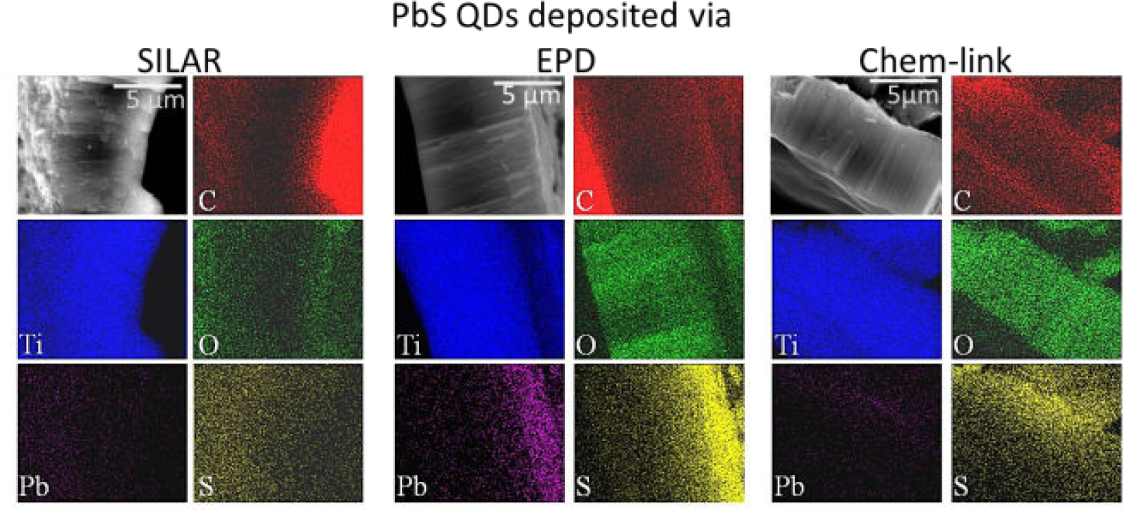
(Scale bar: 5 μm) Scanning electron microscopy-energy dispersive x-ray spectroscopy micrograph and elemental maps of side profiles of TiO2 nanotubes with PbS quantum dots deposited using successive ion layer adsorption and reaction (SILAR), electrophoretic deposition (EPD) or chemical linking (Chem link)

Optical absorption measurements of PbS quantum dots deposited using successive ion layer adsorption and reaction (SILAR), electrophoretic deposition (EPD) or chemical linking (Chem link)
Transmission electron microscopy analysis (Figure 12) was used to determine the size of pre-synthesized quantum dots as 3.96 ± 0.03 nm, and two prominent sizes 2.4 ± 0.6 nm and 4.3 ± 0.3 nm for successive ion layer adsorption and reaction synthesized quantum dots. In addition to size information, the transmission electron microscopy images of quantum dot-functionalized nanotubes shown in Figure 12 also indicate the non-spherical shape of successive ion layer adsorption and reaction quantum dots, and possible agglomeration of the chemically linked quantum dots. Glancing angle x-ray diffraction patterns (Figure 13) of amorphous (unannealed) nanotubes functionalized with quantum dots display broad peaks, typical of nanocrystals, that correspond to the JCPDS card 05–0592 for cubic PbS. The broadness of the peaks is due to the extremely small size, and therefore limited long-range order, of the lattice structure within quantum dots. The prominence of the peak associated with the (200) crystal plane in the successive ion layer adsorption and reaction quantum dot-containing device demonstrates a preferential growth along this axis during the growth process of the quantum dots. The preference for this face also explains the non-spherical shapes observed in the transmission electron microscopy images. The same lattice plane preference is not observed in the electrophoretic deposition and chemical linking devices, which contain colloidal quantum dots.

Transmission electron microscopy images of amorphous TiO2 nanotubes with PbS quantum dots PbS quantum dots deposited using successive ion layer adsorption and reaction (SILAR), electrophoretic deposition (EPD) or chemical linking (Chem link) (Inset: pre-synthesized PbS quantum dots prior to their use in these techniques)

Glancing angle x-ray diffraction patterns of amorphous TiO2 nanotubes with PbS quantum dots PbS quantum dots deposited using successive ion layer adsorption and reaction (SILAR), electrophoretic deposition (EPD) or chemical linking (Chem link)
3.2 Indium-Tin Oxide Quality
Given the importance of the electrical conductivity and optical transparency of the indium-tin oxide in our devices, several figures of merit relating to these values for indium-tin oxide were characterized. The resistivity was determined using a two-point probe system and a Keithley source meter controlled by a custom LabView voltage-sweep program.
In Figure 14A, current density vs. voltage for indium-tin oxide deposited using both electrochemical assistance and electron beam evaporation are displayed. For the indium-tin oxide deposited via electron beam evaporation, the resistivity is 0.0061 ± 0.0006 Ω-cm, which is comparable to other reported values of indium-tin oxide annealed in air [65,68]. For the indium-tin oxide deposited via electrochemical assistance, the resistivity is much higher at 0.0142 ± 0.0003 Ω-cm. The much higher resistivity may lead to limited hole extraction, making indium-tin oxide deposited via electrochemical assistance a less ideal hole extraction material. As is observable in Figure 14B, indium-tin oxide deposited by both techniques is between 70 to 90% transparent throughout nearly the entire solar spectrum, so in terms of light transparency both deposition methods produce indium-tin oxide that is well suited for use as front-contacts in photovoltaic devices.

Percent transmission (A) and IV curves (B) of thin films of annealed indium-tin oxide deposited on glass slides using either electrochemically assisted deposition (EAD) or electron beam evaporation (ebeam)
Utilizing the glancing angle x-ray diffraction patterns of annealed devices shown in Figure 15, the presence of anatase TiO2 and In2O3 was confirmed. Since tin is substitutionally incorporated into the lattice of indium-tin oxide, the diffraction peaks for tin oxide were not expected nor observed in the patterns collected [65,66]. Assuming peak broadening is only due to grain size effects, the average grain size for the oxides are calculated using Scherrer's equation [69].


Glancing angle x-ray diffraction patterns of photovoltaic devices containing annealed TiO2 nanotubes, PbS quantum dots, and indium-tin oxide deposited using either electrochemically assisted deposition (EAD) or electron beam evaporation (ebeam)
For a given peak, β is the full width half maximum in radians, is the Bragg angle, K is a constant usually taken to be 0.9 and λ is the wavelength of incident radiation (0.154056 nm for Cu Kα). For TiO2 the grain size is 19 nm. For the indium-tin oxide-related In2O3 grains, the sizes are 19 nm for indium-tin oxide deposited via electron beam evaporation and 22nm for indium-tin oxide deposited via electrochemical assistance. The grain sizes for the nanotubes and indium-tin oxide deposited by either method are similar and are small compared to the nanotube length (6 μm). Smaller grain sizes indicate more grain boundaries, which act as charge trap sites preventing effective transport through the material.
3.3 Performance Analysis of Solar Cells with Indium-Tin Oxide Deposited via Electrochemical Assistance
As seen in Figure 16, the photovoltaic performance of devices containing indium-tin oxide deposited via electrochemical assistance is minimal with the only device displaying a photoresponse being the one containing chemically linked quantum dots.

Typical current density (A) and power density (B) responses from nine replicates of photovoltaic devices containing TiO2 nanotubes, indium-tin oxide deposited via electrochemical assistance and PbS quantum dots deposited using successive ion layer adsorption and reaction (SILAR), electrophoretic deposition (EPD) or chemical linking (Chem link)
A possible cause for poor device performance is the diminished active area due to limited infiltration of either the quantum dots or indium-tin oxide deposited via electrochemical assistance. To investigate this possibility, scanning electron microscopy and energy-dispersive x-ray spectroscopy were used to analyse side profiles of the devices (Figure 17). The results of the scanning electron microscopy-energy dispersive x-ray spectroscopy elemental mapping of devices reveals that the lack of photoresponse in the successive ion layer adsorption and reaction, and electrophoretic deposition quantum dot devices, arises from two different causes: dissolution of the quantum dots in the case of successive ion layer adsorption and reaction devices and the generation of a separated layer of indium-tin oxide on top of the electrophoretic deposition quantum dot-device.
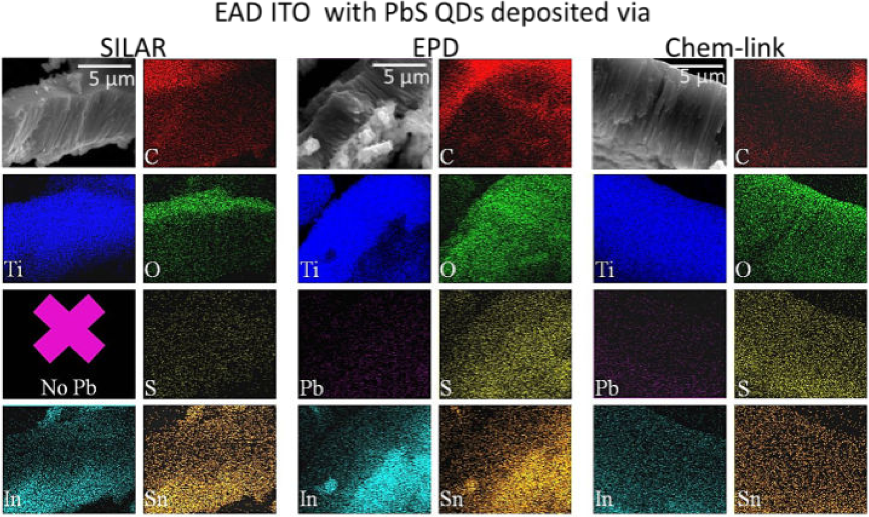
(Scale bar: 5 μm) Scanning electron microscopy-energy dispersive x-ray spectroscopy micrograph and elemental maps of side-profiles of photovoltaic devices containing indium-tin oxide deposited via electrochemical assistance (EAD) and PbS quantum dots deposited using either successive ion layer adsorption and reaction (SILAR), electrophoretic deposition (EPD) or chemical linking (Chem link)
The device containing the successive ion layer adsorption and reaction quantum dots, shown in Figure 17, does not display a Pb signal within the device. Since prior to electrochemically assisted deposition of indium-tin oxide, a Pb signal is observed for all the quantum dot deposition techniques including successive ion layer adsorption and reaction (Figure 10), the probable cause for the signal loss is dissolution of the successive ion layer adsorption and reaction synthesized quantum dots, which are not protected by surface ligands, unlike those deposited by electrophoretic deposition and chemical linking. The following reaction scheme is proposed for the dissolution of successive ion layer adsorption and reaction synthesized quantum dots, resulting in the observed scanning electron microscopy-energy dispersive x-ray spectroscopy maps, which demonstrate no Pb-signal but a definite S-signal.


While typically only trace amounts of PbS dissolve in water, two natural side reactions occur to shift the equilibrium to favour dissolution. First, the sulphide anion, the conjugate base of a weak acid, is consumed in a hydrolysis reaction. Second, at the low pH conditions of electrochemically assisted deposition, initially below 2.3, the solubility of PbS is increased even more by another side reaction, protonation of the sulphide anion [70]. Favouring PbS dissolution by reducing the concentration of dissolved S2−occurs through any combination of reactions 2 and 3, and accounts for the disappearance of the Pb signal. The remaining S signal can be accounted for either by simple re-adsorption of S2− or HS− to the nanotubes or by the final step in the proposed process, which is the reaction of S with surface hydroxide groups, commonly found on unannealed nanotubes, to form titanium hydroxy-sulfide complexes [71,72].
The lack of a quantum dot layer between the oxides may cause the devices to short-circuit and generate the linear-type current response seen in Figure 16. In addition to scanning electron microscopy-energy dispersive x-ray spectroscopy data, calculation of the quantum dot concentration density pre- and post-indium-tin oxide deposition using inductively coupled plasma optical emission spectroscopy (ICP-OES) indicates a reduction in the density of successive ion layer adsorption and reaction quantum dots after electrochemically assisted deposition. Figure 18 contains the comparative analysis of quantum dot-density of devices pre- and post-indium-tin oxide deposition determined using observed Pb concentrations obtained using ICP-OES of devices digested using a 2% nitric acid and 4% hydrogen peroxide solution. The quantum dot concentration density for devices prior to indium-tin oxide deposition are all equal (within uncertainties), indicating the deposition technique utilized to deposit the quantum dots did not impact the amount of quantum dots deposited within the nanotubes in this case. However, the concentration of the quantum dots after indium-tin oxide deposited via electrochemical assistance deposition does vary, especially for the successive ion layer adsorption and reaction quantum dots. The concentration of successive ion layer adsorption and reaction quantum dots decreased by over an order of magnitude after indium-tin oxide electrochemically assisted deposition, confirming that dissolution of the unprotected quantum dots occurred at a higher rate than that of the protected quantum dots.

Quantum dot areal density for devices containing TiO2 nanotubes, PbS quantum dots deposited using successive ion layer adsorption and reaction (SILAR), electrophoretic deposition (EPD), or chemical linking (Chem link), and either no indium-tin oxide or indium-tin oxide deposited using electrochemically assisted deposition (EAD) or electron beam evaporation (ebeam). Quantum dot concentration based on Pb content obtained from acid-digested devices using ICP-OES and assuming PbS quantum dot density is equal to the PbS bulk density of 7.16 g/cm3.
Unlike the successive ion layer adsorption and reaction quantum dot device, the devices containing quantum dots deposited using electrophoretic deposition and chemically linked quantum dots, still display a uniformly distributed Pb-signal along the length of the nanotube array in scanning electron microscopy-energy dispersive x-ray spectroscopy elemental map and the same concentration of quantum dots before and after indium-tin oxide deposited via electrochemical assistance deposition. The cause of the poor photo-response for the electrophoretic deposition device is a lack of infiltration of the indium-tin oxide. The In-signal in the scanning electron microscopy-energy dispersive x-ray spectroscopy maps (Figure 17) while extending throughout the device show a large collection of In-containing material covering the top of the device but not interfacing within the nanotubes. Colloidal PbS quantum dots are surrounded by surface-passivating, hydrophobic ligands; the presence of these ligands may limit the infiltration of the aqueous solution used during electrochemically assisted deposition of indium-tin oxide. To determine the hydrophobicity of nanotubes functionalized with PbS quantum dots, the advancing contact angle of a drop of water on the surface of nanotube arrays functionalized with quantum dots was observed.
The results shown in Figure 19 indicate that the array functionalized with quantum dots deposited using electrophoretic deposition has the highest contact angle at slightly greater than 118°. However, the array with the chemically linked quantum dots also has a comparably higher contact angle, which is to be expected since only a partial exchange of the surface ligands occurs during chemical linking. It does indicate that the cause of the exclusion of the indium-tin oxide in the electrophoretic deposition device is more complex than hydrophobicity issues alone. Plan-view scanning electron microscopy micrographs of nanotubes functionalized with quantum dots are shown in Figure 20 and reveal the main reason for the exclusion of indium-tin oxide from the TiO2 pores in the electrophoretic deposition device. The nanotubes are almost completely sealed by quantum dots at the tops of the nanotubes. The separation of the indium-tin oxide from the rest of the photovoltaic device causes a break in the circuit and results in the minimal current observed for the electrophoretic deposition devices seen in Figure 16.
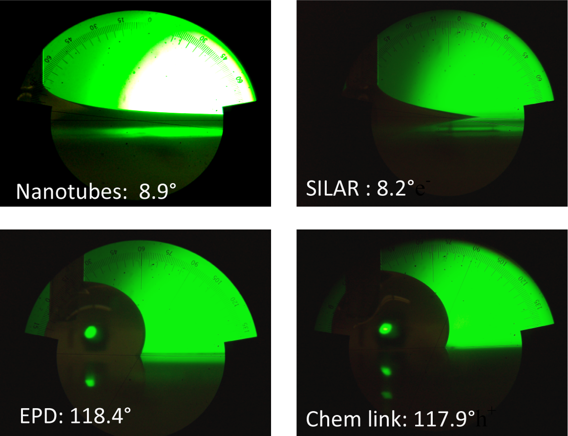
Images of advancing contact angle measurements (with the average of triplicate measurements) of water drops on the surface of bare nanotubes and of nanotubes with PbS quantum dots deposited using successive ion layer adsorption and reaction, electrophoretic deposition or chemical linking

(Scale bar: 3 μm) Plan-view scanning electron microscopy micrographs of nanotube arrays sensitized with PbS quantum dots using either successive ion layer adsorption and reaction (A), electrophoretic deposition (B) or chemical linking (C)
While the devices containing chemically linked quantum dots and indium-tin oxide electrochemically assisted deposition exhibit a photovoltaic response (Figure 16), the power generated is very small. One possible cause for the poor performance is revealed upon analysis of the topography of the indium-tin oxide. Plan-view scanning electron microscopy micrographs of annealed devices are shown in Figure 21. Large cracks are generated due to evaporation of the solvent used to deposit indium-tin oxide deposited via electrochemical assistance and residual stress generated during annealing. The cracks act as charge barriers limiting or preventing charge collection across the top of the film. Another interesting aspect of the cracking is that the device containing quantum dots deposited using electrophoretic deposition and indium-tin oxide deposited via electrochemical assistance (Figure 21B) does not show any correlation between the cracks in the nanotube array and the cracks in the indium-tin oxide film; another indication that the indium-tin oxide is not interfaced with the rest of the photovoltaic device.

(Scale bar: 3 μm) Plan-view scanning electron microscopy micrographs of annealed photovoltaic devices containing indium-tin oxide deposited via electrochemical assistance PbS quantum dots deposited using either successive ion layer adsorption and reaction (A), electrophoretic deposition (B) or chemical linking (C)
3.4 Performance Analysis of Solar Cells with Electron Beam Evaporated Indium-Tin Oxide
Electron beam evaporated indium-tin oxide (indium-tin oxide deposited via electron beam evaporation), which was deposited by thermal evaporation and subsequent condensation of an indium/tin target, does not involve the solution-based chemistry that led to the deleterious interactions with the quantum dots observed with indium-tin oxide deposited via electrochemical assistance. Figure 22 displays the photovoltaic response of devices containing PbS quantum dots and indium-tin oxide deposited via electron beam evaporation. Overall, the performance is greatly enhanced compared to that of devices containing indium-tin oxide deposited via electrochemical assistance (Figure 16), but is still below viable efficiency for use as commercial devices.

Typical current density (A) and power density (B) responses from nine replicates of photovoltaic devices containing TiO2 nanotubes, indium-tin oxide deposited via electron beam evaporation, and PbS quantum dots deposited using either successive ion layer adsorption and reaction, electrophoretic deposition or chemical linking
The observed enhancement could be attributed to a multitude of reasons. As seen in Figure 18, the concentration density of quantum dots remains unchanged after the deposition of indium-tin oxide deposited via electron beam evaporation for all devices, confirming that transitioning from the solution-based deposition of indium-tin oxide deposited via electrochemical assistance to the vapour deposition of indium-tin oxide deposited via electron beam evaporation prevented the detrimental dissolution of the PbS quantum dots. As the PbS quantum dots act as both the light harvester and as a physical barrier preventing charge-carrier recombination between the two oxides, any technique that decreases damage to the quantum dots will enhance their ability to perform within the photovoltaic devices.
The topography of the indium-tin oxide deposited via electron beam evaporation, displayed in the plan-view scanning electron microscopy images in Figure 23, is much more uniform than that observed with indium-tin oxide deposited via electrochemical assistance, shown in Figure 21. Ebeam indium-tin oxide shows only minimal cracking and no particulate-like formations. Since cracking and particle-to-particle percolation increase charge-trapping, the improved topography of the indium-tin oxide deposited via electron beam evaporation also contributes to the enhancement of the photoresponse of these devices compared to those containing indium-tin oxide deposited via electrochemical assistance. In addition to decreasing the number of potential charge-trapping sites, the reduction of cracking in the indium-tin oxide deposited via the electron beam evaporation device may also indicate a more complete indium-tin oxide layer surrounding the quantum dots, which could limit air exposure of the quantum dots and increase the viable lifetime of the quantum dots as light-harvesters.

(Scale bar: 3 μm) Plan-view scanning electron microscopy micrographs of photovoltaic devices containing TiO2 nanotubes, indium-tin oxide deposited via electron beam evaporation, and PbS quantum dots deposited using successive ion layer adsorption and reaction (A), electrophoretic deposition (B) or chemical linking (C)
Although evaporation of indium-tin oxide reduces side-reactions associated with aqueous solution-based deposition and generates smoother films, evaporation from a point source can cause limited pore infiltration of materials into high-aspect-ratio structures. To evaluate the infiltration, scanning electron microscopy-energy dispersive x-ray spectroscopy maps of side profiles of indium-tin oxide deposited via electron beam evaporation-containing devices (Figure 24) were analysed. The low deposition rate of ∼0.5 Å/s appears to allow infiltration of indium-tin oxide into the pores in all of the devices. The device containing quantum dots deposited using electrophoretic deposition still displays some occlusion of the indium-tin oxide, owing to the partial sealing of the nanotubes by excess quantum dots. However, unlike indium-tin oxide deposited via electrochemical assistance, indium-tin oxide deposited via electron beam evaporation does appear to infiltrate the electrophoretic deposition quantum dot-functionalized nanotubes, likely due to the fact that hydrophobicity does not play a role during electron beam evaporation deposition.

(Scale bar: 5 μm) Scanning electron microscopy-energy dispersive x-ray spectroscopy of photovoltaic side profiles with indium-tin oxide deposited via electron beam evaporation and PbS quantum dots deposited using successive ion layer adsorption and reaction (SILAR), electrophoretic deposition (EPD) or chemical linking (Chem link)
4. Conclusions and Future Prospects
Looking toward future optimal devices, combining the best device fabrication routes found here with recent advances in implementing quantum dots into solar-harvesting devices, which have come to rival the efficiencies of commercial Si and dye-sensitized solar cells, could be the archetype for future success. Bawendi constructed a PbS quantum dot thin film device with a certified efficiency of 8.55% [73]; it is not a typical quantum dot-sensitized solar cell, since charge generation and migration occur within the same material, but the meticulous bandgap engineering used to construct the device is similar to the energetic separation implemented in a quantum dot-sensitized solar cell. It may just be possible that an even higher efficiency and better commercial-viability could be achieved by employing the same bandgap engineering and equivalent materials in a quantum dot-sensitized solar cell, especially if self-assembly of ordered sizes of quantum dots are employed to make a rainbow, tandem cell configuration like that shown in the artistic rendition in Figure 25.

Artistic impression of quantum dot-sensitized solar cell utilizing ligand-modulated bandgap engineering, rainbow cell quantum dot size progression, and tandem cell design to maximize efficiency. From the bottom up the cell comprises a transparent conductive oxide substrate, coated with a metal contact, a self-assembled monolayer of cysteine, a single layer of TiO2 particles functionalized with TBAI, a layer of TBAI-capped large size quantum dots, a layer of EDT-capped smaller size quantum dots, an interfacial layer, followed by the top cell which starting with the TiO2 layer is identical to the bottom cell, with the exception that the quantum dots are smaller and the final structure is completed with indium-tin oxide.
By utilizing a self-assembled monolayer of ligands on metal-substrates, for example cysteine, which have been shown to facilitate charge migration in quantum dot-sensitized solar cell [74] on Au, a single layer to a few layers of TiO2 could be deposited through chemical linking, limiting carrier recombination during percolation. The TiO2 layer should be modified with an inorganic halide ligand, such as tetrabutylammonium iodide (TBAI), which Bawedi [73] utilized to create the bandgap offset ideal for charge separation, or one of the other commonly utilized ligands to manipulate the quantum dot band structure [75-77]. The TiO2 layer should then be decorated with a large-size quantum dot capped with the same inorganic halide and then with a slightly smaller quantum dot capped with a thiol, such as thioglycolic acid or 1,2-ethanedithiol (EDT), to further encourage charge separation through bandgap modulation, utilizing the well-known bandgap modulation through size adjustment [78,79] and the added benefit that larger sized quantum dots have fewer accessible trap sites [80]. An interfacial layer, Au islands or conformal indium-tin oxide film, separates the two cells. The entire cell should be completed with conformal film of indium-tin oxide. Thus, the cell architecture facilitates charge-transfer similar to plants through physical and energetic separation of charge-carriers and takes advantage of enhanced solar collection through utilization of progressive sizes of quantum dots, like that of the Rainbow cell proposed by Kamat [81-84]. The other advantage of the prospective architecture is that it is a tandem cell, utilizing the power of multiple cells connected in series to improve the output efficiency [85]. The commercial advantage of the prospective cell is that it is an easily scalable, solution-based fabrication process that given the appropriate substrates could even be readily adapted to roll-to-roll processing [86] or cell printing [87]. The key to the efficiency demonstrated by photosystem I and potentially achievable with quantum dot-sensitized solar cell is the efficient separation of carriers over macroscopic distances. The key for producing a commercially viable quantum dot-sensitized solar cell is the realization of this separation utilizing readily abundant, cost-effective materials [88]. Although the exact cell architecture with the appropriate molecular wiring has yet to be realized for a quantum dot-sensitized solar cell, the current body of research provides a deluge of supporting steps that if combined appropriately will yield the quantum dot-sensitized solar cell to rival nature's photosynthesis.
Footnotes
5. Acknowledgements
T.W. would like to thank the VINSE community for intellectual support, especially Drs. Jeremy Mares and Gabriel Leblanc. This work was supported by grants from the National Science Foundation (EPS-1004083) (TN-SCORE), (DMR-0957701) and (CHE 1213758).