
Abstract
Field emission and current noise of hydrothermally synthesized MoS2 nanosheets are investigated in ultra-high-vacuum and industrially suited high-vacuum conditions. The study reveals that the emission turn-on field is pressure dependent. Moreover, the MoS2 nanosheets exhibit more stable field-electron emission in high-vacuum than in ultra-high-vacuum conditions. The investigations on field-emission current fluctuations show features of 1/f-type noise in ultra-high-vacuum and high-vacuum conditions, attributed to adsorption and desorption processes. The post-field-emission results indicate the MoS2 nanosheets are a robust field emitter in high-vacuum conditions.
1. Introduction
Of late, advances in the area of two-dimensional (2D) materials like graphene and its inorganic analogues have attracted a great deal of research attention because of their promising applications in various electronic devices owing to their exotic physicochemical properties. One of these materials, molybdenum disulphide (MoS2), has been explored for a variety of applications including field-effect transistors [1-3], phototransistors [4], sensors [5-7], integrated circuits [8, 9], and field emission [10-12]. We recently observed that MoS2 with several layers exhibits excellent field-emission properties in an ultra-high vacuum (UHV) [10]. However, to ensure practical applicability of a field emitter it is necessary to understand its current stability and noise/fluctuations in industry-suited high-vacuum conditions (∼10−6 mbar). The noise provides the information regarding its source. Especially the 1/f type of noise reflects many processes at the electronic and atomic level, and thus is an evaluating parameter for reliability of the device [13]. Therefore, we have investigated field-emission properties and current noise from hydrothermally synthesized MoS2 nanosheets in UHV (P∼3×10⁻⁸ mbar) and high-vacuum (HV: P∼1×10⁻⁶ mbar) conditions.
2. Experimental procedure
MoS2 sheets were synthesized by a one-step hydrothermal reaction. In a typical experiment, 3 mM Na2MO4(Sigma-Aldrich, 99.98%) and 15 mM thioacetamide (C2H5NS, Sigma-Aldrich, ≥ 99%) were dissolved in 40 mL DI water and stirred for one hour at room temperature using a magnetic stirrer. The solution was transferred to a 50 mL teflon-lined stainless-steel autoclave, heated up to 200°C and left for 24 hours. After cooling naturally, the product was filtered, washed with DI water and dried in a vacuum at 60°C for six hours. The as-synthesized product was then characterized by Raman spectroscopy, Transmission Electron Microscopy (TEM) and Field Emission Scanning Electron Microscopy (FESEM). The Raman spectrum was recorded with high-resolution Raman spectrometer (LabRAM HR Horiba Jobin Yvon) using 514 nm as excitation wavelength at room temperature.
For field-emission measurements, as-synthesized MoS2 nanosheets were ultra-sonicated in ethanol for 10 minutes. The nanosheets were solution cast on pre- cleaned Si substrate (∼1 cm2). The field-emission investigation of MoS2 nanosheets on Si substrate was carried out in a diode configuration in both UHV and HV conditions. In the diode configuration, the specimen (MoS2/Si, cathode) was mounted parallel to a semi-transparent conducting phosphor screen (Cu-doped ZnS, the anode), at an interelectrode separation of ∼500 μm. The field-emission current (I) versus applied voltage (V) measurements were carried out using an electrometer (Keithely 6514) and a high-voltage dc power supply (Spellman, 40 kV). The field-emission current stability was recorded at the pre-set current value of 1 μA using a computer-controlled data-acquisition system, with a sampling time of 10 s. The field-emission current-time traces and the corresponding power spectra were recorded using a Fast Fourier Transform (FFT) analyser (IWASTU SM-2701). The results were reproducibly repeated for two different specimens prepared under identical conditions.
3. Results and discussion
Figure 1 shows the Raman spectrum of the as-synthesized MoS2 nanosheets, depicting the fingerprints of in-plane vibrational mode as E12g at ∼ 378 cm−1 and out-of-plane vibrational mode as A1g at ∼404 cm−1 of MoS2. Careful observation of the spectrum reveals appearance of a shoulder at ∼ 384 cm−1 near the E12g peak, which may be attributed to defects present in MoS2.
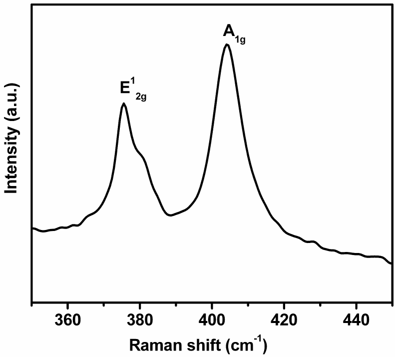
Raman spectrum of as-synthesized MoS2 nanosheets
Figures 2 (a-b) show low- and high-magnification TEM images of the MoS2 nanosheets, respectively. The average dimension of the nanosheets is found to be 1–3 μm. Figures 2 (c-d) show the FESEM images of solution-cast MoS2 nanosheets on Si substrate. The images clearly reveal the presence of a number of protruding edges, which act as emission sites.

(a-b) Low- and high-magnification TEM images, and (c-d) FESEM images of MoS2 nanosheets
The field-emission current-density (J) versus applied-electric-field (E) plots of MoS2 nanosheets in HV and UHV are shown in Figure 3(a). The values of the turn-on field required to draw emission current density of 1 μA/cm2 in HV and UHV conditions are found to be 10.8 and 11.6 V/μm, respectively. Figure 3(b) shows the corresponding Fowler-Nordheim (F-N) plots (a plot of ln (J/E2) versus 1/E) derived from the J-E plots of MoS2 nanosheets in HV and UHV conditions. Both the F-N plots show a linear nature over the entire range of the applied field. Figures 4(a-b) depict the field-emission current stability of MoS2 nanosheets recorded in HV and UHV, respectively. The emission current in UHV exhibits an initial rise and further stabilization at a 2 μA current level. The observed initial rise in the current is attributed to the preconditioning of the specimen due to residual gas ion bombardment [14]. The magnitude of the standard deviation around the mean value is found to be 0.15 and 0.24 μA for the emission current in HV and UHV, respectively, indicating that MoS2 nanosheets exhibit relatively stable behaviour in HV compared to UHV. In UHV and HV conditions, the typical number density of molecules is of the order of ∼108 and 1010 molecules/cm3, respectively. The time to form a monolayer is ∼73 s in UHV and ∼2.2 s in HV [15]. In UHV conditions, the coverage of adsorbing gas molecules on the surface of MoS2 nanosheets is much less in comparison with HV conditions. The continuous ion bombardment during the operation of the emitter desorbs the adsorbed gas molecules from the surface of the emitter in UHV conditions. In HV conditions, the coverage of the adsorbing molecule is high enough that it is not altered due to ion bombardment. Therefore, in UHV, the temporal changes in work function due to adsorption/desorption events lead to more deviations from the average value of the current (Figure 4a) than re observed in the HV conditions (Figure 4b). This is also reflected in the values of standard deviation, as discussed above. The field-emission patterns were recorded at ∼50 μA and are shown in Figures 4 (c-d). The field-emission pattern observed in the HV conditions exhibits brighter emission spots than in the UHV. The observed spots indicate that the emission comes from the sharp protrusions on the edges of the MoS2 nanosheets (as seen in FESEM images, Figures 2 (c-d)).
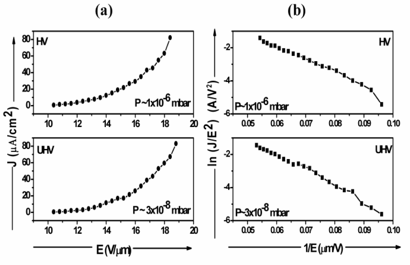
(a) J-E plots and (b) F-N plots of MoS2 nanosheets on Si substrate in HV and UHV, respectively
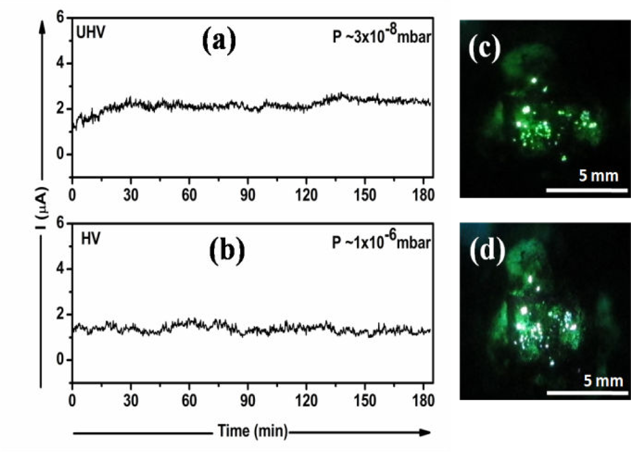
Field-emission current stability at the pressure of (a) P∼3×10⁻⁸ mbar, (b) P∼1×10⁻⁶ mbar. Field-emission patterns recorded at ∼50 μA of MoS2 nanosheets at the pressure of (c) P∼3×10⁻⁸ mbar, (d) P∼1×10⁻⁶ mbar
To gain an understanding of the origin of the observed fluctuations in the emission current (noise), the FFT analyser was used. Figures 5 (a-b) depict the current time traces and Figures 5 (c-d) show the corresponding power spectra of MoS2 field emitters operated in UHV and HV, respectively. Figures 5 (a-b) show that the MoS2 field emitter exhibits step-like fluctuation, indicating ‘flip-flop’ behaviour between two states in the UHV environment, and between multiple states in the HV environment. The power spectra corresponding to the current time traces reveal 1/fα-type behaviour, with α ∼0.86 and 0.98 in UHV and HV, respectively. In HV, the emitter is covered with residual gases, and in such a case α ∼1 [15]. α is less than 1 for UHV, as found in the present case. These fluctuations may be related to surface diffusion. The observed ‘flip-flop’ can be treated as switching between two or more adsorption states mediated by surface diffusion, as modelled by Klient [16].
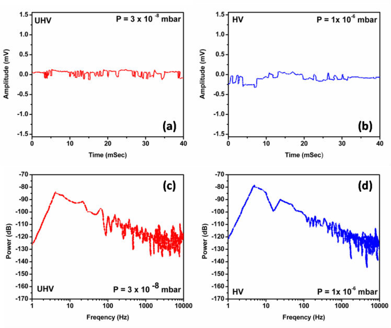
Field-emission current-time traces recorded at (a) P ∼ 3×10⁻⁸ mbar, (b) P ∼ 1×10⁻⁶ mbar, at the preset value of 1 μA, and the corresponding power spectra recorded at (c) P ∼ 3×10⁻⁸ mbar, (d) P ∼ 1×10⁻⁶ mbar
After taking the field-emission measurements, we further investigated the surface morphology of the MoS2 nanosheets by FESEM (shown in Figures 6(a-b)). It is interesting to note that the surface morphology shows no significant deterioration after long-term operation, even in HV conditions. The results indicate that the MoS2 nanosheets constitute a robust field emitter.
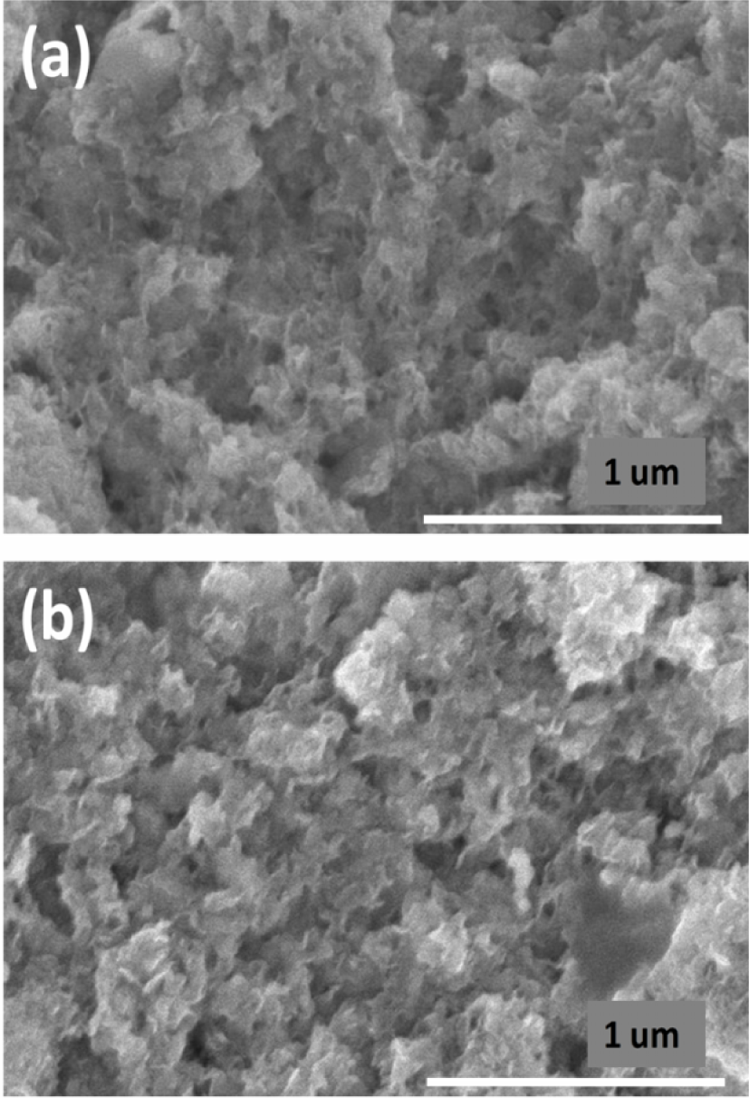
FESEM image of MoS2 nanosheets, (a) pre field emission, (b) post field emission measurements
4. Conclusions
The investigation of field-emission current noise shows features of 1/fα noise in UHV and HV conditions, with α ∼ 0.86 and 0.98, respectively. The temporal variations in the local work function are due to the adsorption-mediated surface diffusion. The MoS2-nanosheets emitter exhibits significant stable emission current in HV conditions. The MoS2 nanosheets prove to be robust in the industry-suited vacuum environment.
Footnotes
5. Acknowledgements
RVK would like to thank the Council of Scientific and Industrial Research (CSIR), New Delhi, India, for the SRF Scheme. DJL would like to thank the Department of Science and Technology (DST), Govt. of India, for the award of a Ramanujan Fellowship. Thanks are also due to Prof. D. S. Joag, Emeritus Scientist-CSIR, Department of Physics, University of Pune, for useful discussions. This field-emissions work has been carried out as part of the CNQS-UPE-UGC programme.