
Abstract
This paper presents a discrete-time decentralized control scheme for trajectory tracking of a two degrees of freedom (DOF) robot manipulator. A high order neural network (HONN) is used to approximate a decentralized control law designed by the backstepping technique as applied to a block strict feedback form (BSFF). The weights for each neural network are adapted online by an extended Kalman filter training algorithm. The motion for each joint is controlled independently using only local angular position and velocity measurements. The stability analysis for the closed-loop system via the Lyapunov approach is included. Finally, the real-time results show the feasibility of the proposed control scheme robot manipulator.
1. Introduction
Although carbon nanofibers might have been discovered as early as 1889 [1], two major breakthroughs brought life to this artless material. In 1985, Buckminster fullerene C60 was discovered by a team headed by Kroto [2] followed by the illustration of IIjima [3] that carbon nanotubes are formed during the arc discharge synthesis of C60. These illustrations encouraged scientists to look into the applications of this exciting material. Today, carbon nanofiber research has a never ending horizon with application in the fields of biology, medicine, astronomy, electronics, etc. The main factors accounting for this tremendous attention are properties such as high electrical and thermal conductivities, superior mechanical strength, a wide electrochemical potential, flexible surface chemistry and biocompatibility [4–5]. In the field of electronics, the main research focuses on the integration of carbon nanofibers onto a chip. Vertically Aligned Carbon Nano Fibers (VACNFs) grown and patterned on substrates have already received enormous attention due to their high spatial and temporal resolution, and surface functionalization. Recent progress in micro and nanofabrication technologies have enabled the integration of electrodes such as microelectrode arrays [6] and interdigitated arrays (IDA) [7] with materials such as carbon nanofibers [8–9], carbon nanotubes [10–11], silicon nanowires [12] and diamond nanowires [13–14]. Of the different available fabrication methods, catalyst enhanced Plasma Enhanced Chemical Vapour Deposition (PECVD) is the most commonly used for its reliability in the iteration of the process. With few processes in fabrication that are still operated manually, a level of progress has been seen in chip integration as well as the growing of fibers uniformly. With wet bench technologies still in place, during VACNF growth, they are exposed to a variety of chemicals, especially acids. Thus, there is much need to understand the effects of different acids on the VACNFs in order to facilitate the growth of uniform sized and shaped fibers for chemical and biosensor development.
2. Atomic Force Microscopy
Atomic Force Microscope (AFM) is a very high resolution type of scanning probe microscope that works on the principle of beam deflection and has fractions of a resolution of a nanometre. The advantages of AFM over Scanning Electron Microscopy (SEM) are its ability to generate the 3-D images unlike the two dimensional images from SEM, maintain sample integrity and operate in air unlike the vacuum for SEM. With the ability to operate in different modes such as contact, lateral force microscopy, non-contact, tapping and phase imaging, AFM can scan almost any type of surface, and thus AFM is used extensively in material research including for materials such as polymers, ceramics, composites, glass, and biological samples. A probe on the microscale cantilever beam attached to the objective lens will scan the surface of the sample. A beam deflection system consisting of a laser and photodetector is built into the microscope to measure the position of the beam and ultimately the position of the cantilever tip. To calculate the force, Hooke's Law, F= -kz (where F is the force, k is the spring constant of the cantilever, and z is the displacement of the cantilever) is used. The laser beam is placed on the cantilever tip and the beam deflection measures the displacement the sample exerts on the cantilever. The spring constant is known based on what type of scanning probe is used. Owing to the above stated advantages, AFM is used in this study to evaluate the effects of etching on VACNFs by inorganic and organic acids during chips processing.
3. Fabrication of VACNF Electrode Chips
VACNFs Nano Electrode Arrays (NEAs) were fabricated at NASA Ames Research Center which includes six major steps as shown in Fig. 1 [15]. The first major step is the metal deposition. Electron beam evaporation is used to deposit a 200 nm thick Cr film and then the wafer is cleaned with acetone, methanol and Isopropyl alcohol. Metal deposition is followed by a patterning of Ni dots. E-beam lithography is used for the patterning of the deposited metal such that approximately 39,000 Ni dots are patterned for each array. After the Ni dots are patterned, VACNFs are grown using a Direct Current (DC)-biased PECVD. Each individual CNF is vertically grown and patterned on the surface with a Ni catalyst on each tip. Operating deposition for 15 minutes will produce CNFs of a height of 1.5μm, a base diameter of 100nm and a tip diameter of 70 nm on average. Followed by directional CNF growth, a 3μm layer of Silicon Dioxide (SiO2) is deposited in order to passivate the side walls of the grown carbon nanofibers. For this process, dual RF etching and PECVD are used to obtain a high conformal coating of SiO2. Surface polarization along with the exposing of the nanofiber tips is attained using Chemical Mechanical Polishing (CMP), by removing excess SiO2 and partial removing the nanofiber tip. The last step in the fabrication process is the treatment of the fibers with different etchants / acids in order to expose the contact pads and partially remove the CNFs. SEM scans of the VACNFs pre and post etch – post CMP are shown in Fig. 2 (e) and (f) respectively. Clearly, while the CMP had retained a flat surface, etching had made the surface rough. A high temperature driven CVD growth had resulted in the growth of multiple fibers at a single location as shown in Fig. 2(c). This led to nanofibers being grown in a more disorderly manner with more than one fiber observed at a single location.

Schematic showing the steps involved in the unetched and etched fabrication of VACNFs.

Actual SEM images captured during the fabrication procedure. a,b,c – grown VACNFs at a 30° angle view d) VACNFs top view e) post etch f) post chemical mechanical polishing.
The etching step in the actual fabrication was used as the final step to remove the oxide layer on the contact pads. Hence one needs to understand extent of the effect of the acids on VACNFs that will be used to remove those oxide layers. In order to determine the effect of the etchant on the carbon nanofibers and the silicon dioxide, the etch rate is calculated using equation (1). The higher the etch rate, the higher the effect of the etchant on the carbon nanofibers and it cannot be employed for etching the surface of the Si wafer. All the samples used for the current experiment are from a single wafer in order to make sure all the wafers are from the same processing conditions and with almost similar dimensions
4. Experimental Setup
The fabricated chips are now treated in a wet bench with different inorganic and organic acids. For the purpose of treatment, three inorganic acids are used, namely sulphuric acid (H2SO4), hydrochloric acid (HCl) and hydrofluoric acid (HF), and an organic acid, namely, acetic acid (CH3COOH), is used. Both HCl and H2SO4 are used at a concentration of 5N while the HF is used at 0.1N. Acetic acid is used at a concentration of 5N. Electrode chips containing VACNFs are measured for their initial fiber dimensions and then dipped into the acid solution for a 5-minute-long treatment. It is the approximate needed time to remove SiO2 from the substrate using HF, and five minutes is regarded as the standard. It is followed by a dump rinse, air cleaning, and drying in a dry box until the relative humidity in the dry box falls below 5%. Once dried, the chips are measured for changes in the fiber dimensions using the Atomic Force Microscope. These changes in the dimensions are caused by the acid and using equation 1, the etch rate is calculated.
The AFM used in the experiment is an Agilent 5500-ILM highly sensitive microscope as shown in Fig. 3. The scanning and characterization were carried out under Acoustic AC imaging mode as shown in Fig. 4. The AFM probe utilized during the imaging has a resonant frequency of 190 kHz and a spring constant of 48 N/m. During intermittent contact, the tip is brought close to the sample, so that it comes into light contact with the surface at the bottom of its travel, causing the oscillation amplitude to drop. Hence, the influence of the cantilever tip during the measurement of the dimensions is ignored since it does not change the shape of the target.

AFM-based experimental setup showing the sample holder and chips for scanning and characterization.

Scan in AC mode: a. tip under sinusoidal motion (1) AC from nose cone, (2) the base body of cantilever, (3) cantilever with tip; b. oscillation amplitude driven by (1); c. reduction from the interaction with sample as a feedback signal to maintain constant amplitude.
5. Experimental Results
A. Scanning and Measurement
By measuring the dimensions of the nanofiber before and after treatment with acid, the effect of the acid on the dimensions of the nanofiber was evaluated. At first, a 5μm square was scanned to find the nanofibers in the area. Then a 2 μm square area was specifically selected in which nanofibers were found, and was rescanned. When a fiber appeared clearly in a scan topography image, a straight line was drawn in any direction in the 2-dimensinal topography image to cross the targeted nanofiber. At the same time, the vertical information along the line was obtained to complete a measurement. This procedure was repeated until an adequate amount of data was collected before starting another measurement.
Figures 5 and 6 are 2-D and 3-D images, respectively, of the untreated surfaces generated using AFM by running a tapping mode probe on the substrate surface at one line/sec. From the images it can be observed that the nanofibers are irregularly arranged while the shapes of the fiber are distinguished from the 3-D image generated as they can be seen in all planes. The 3-D image is generated using picoImage software, which is one of the strong capabilities of the AFM. After the identification of the fiber, a line is drawn over the nanofiber as shown in Fig. 7. While the bulge in the image is the nanofiber, the distance between the two ends where the curve coincides with the base line is considered the diameter of the fiber. The distance from the base line to the highest point in the curve is considered the height of the nanofiber. This process is repeated at 75 different locations on the substrate, and the dimensional data is averaged for precision and accuracy.

2-D image of the unetched surface showing the VACNFs.

A 3-D view of VACNFs over unetched substrate surface.
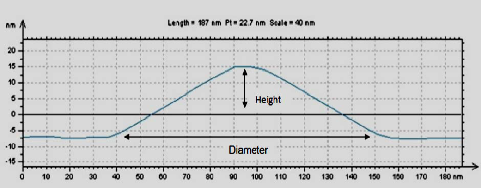
Cross section information for measurement based on line crossing.
Figures 8–11 are the images of the acid treated surfaces. With one look at the images, one can predict that the acids have a huge impact on the dimensions of the fibers. While the treatment with acetic acid had made the nanofibers sharper, treatment with sulphuric, hydrofluoric and hydrochloric acids have resulted in blunt nanofibers. For the untreated substrate, the nanofiber measurements are taken at 75 different locations on the substrate and averaged. Using equation (1), etch rates are calculated for each acid and the results are tabulated in Table 1. Table 1 also shows the mean diameter and height of 75 untreated and acid treated fibers.
Dimensions and Etch Rates of Untreated and Acid Treated VACNFs

Average diameter and height are in nm.
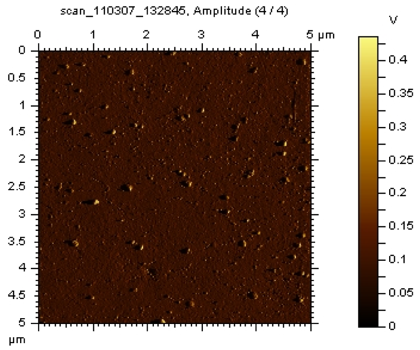
A 5 micron square scanned surface after the treatment with acetic acid. All the dots in the pictures are the free standing nanofibers.

3- D image of the scanned surface after the treatment with acetic acid. The spikes like formations that are protruding out of the surface are the vertically aligned carbon nanofibers.

2-D scan image of the substrate after treatment with sulphuric acid. All the bulged dots in the picture are the nanofibers.

3-D image of the scanned surface after the treatment with 5 N sulphuric acid (H2SO4), which is clearly evident that the edges of the VACNFs are blunt compared to the before treatment pictures and acetic acid treatment pictures.
SEM images of the etchant treated substrate surfaces were obtained to further verify the presence of carbon nanofibers. For this purpose, a Philips EL 20 SEM was used at 10−5mBar and an electron ray of 30 KeV was shot. All the images scanned were 10 μm × 10μm. Fig. 12 A, C and E show the SEM images that were generated from the etchant treated substrates. Energy Dispersive Spectroscopy (EDS) was performed to verify the composition of the etchant treated surfaces. Fig. 12 B, D and F presents the EDS images of the etchant treated surfaces. Fig. 12 (A) shows the Hydrochloric Acid (HCl) treated surface. VACNFs were clearly observed as the illuminating dots in the Silicon Dioxide (SiO2) which forms the dark background. EDS is then performed on the surface and the EDS spectrum is shown in Fig. 12 (B). Peaks for Carbon (C), Oxygen (O) and Silicon (Si) were seen clearly from the spectrum. Since the substrate surface is composed of SiO2, both Silicon and Oxygen will have the highest peaks and are hence seen in the spectrum. Fig. 12 (C) shows the SEM image of the surface treated with sulphuric acid (H2SO4). VACNFs were seen as the illuminating dots in the image. EDS was then performed on the surface to further verify the composition of the surface and is shown in Fig. 12 (D). An acetic acid (CH3COOH) treated surface was scanned under the SEM and an image was generated, as shown in Fig. 12 (E), while the EDS of the surface is shown in Fig. 12 (F). From the SEM images, it can be clearly seen that the Acetic acid treated surface retained the maximum number of fibers and sulphuric acid had an adverse reaction on the surface of the chip and the fibers even became bulged after the treatment with the sulphuric acid. From the EDS spectrum peaks of Carbon, it could be concluded that the acetic acid treated surface had the highest Carbon peak and the sulphuric acid treated surface had the lowest peak. The results of the dimensions also supported the fact that the Acetic acid treated surface had a height increment and a thinning of the diameter. Another reason for the observed peaks was the fact that the acetic acid treated surface had retained the most nanofibers compared to other acid treated surfaces.

A, C, E SEM scan images of the acid treated surfaces. B,D,F EDS performed on the scanned surface to obtain the composition. A. HCl treated substrate surface as seen in the SEM. B. EDS performed on the HCl etched surface. C. H2SO4 etched substrate surface as seen in the SEM. D. EDS performed on the H2SO4 etched surface. E. Acetic Acid etched substrate surface as seen in the SEM. F. EDS performed on the Acetic Acid etched surface
The increase in the height of the CNFs when treated with acetic acid may be due to an initial partial oxidation, leading to the formation of acid functionalized nanofibers which then reacted with the remaining acetic acid to form a bonding and thus increase the height.
B. Statistical Analysis
In statistics, a confidence interval (CI) is an interval estimate of a population parameter. Thus, confidence intervals are used to indicate the reliability of an estimate. As such, a statistical method is used on the experiments to obtain the interval to describe the size of the fibers. 95% confidence is chosen for the purposes of this analysis. The mean diameters of unetched and HF treated are 204.66 nm and 205.509 nm, respectively, while their standard deviations are 25.03 nm and 28.14 nm, respectively. The confidence interval is calculated using equation (2) [16] as.
where, X̅ is the mean values of the samples; Z, the critical value equal to 1.96 in a 95% CI; σ is the standard deviation and N is the number of the samples.
Therefore, for the untreated chips with a mean diameter of 205.529 nm and a standard deviation of 25.03 nm, the confidence interval is [199.86 nm, 211.19 nm] while for the HF treated with a mean diameter of 205.529 nm and a standard deviation of 28.14 nm is [199.16 nm, 211.86 nm]. Similarly, calculating the confidence intervals for heights of unetched and HF etched chips, [18.78 nm, 22.06 nm] and [7.73 nm, 9.08 nm] are obtained, respectively. A summary of the calculated confidence intervals, mean and standard deviation for all unetched and etched chips is shown in Table 2.
Calculation Results of CI for The Sizes of Untreated and Acid Treated VACNFs

All dimensions are in nm.
6. Discussion
From the values shown in Table 1, one can infer that while organic acid resulted in an increase in the nanofiber's height, inorganic acids resulted in etching off from the fiber's height. Additionally, for the diameter data, the pattern is reversed, i.e., while the organic acid resulted in a decrease in the fiber's diameter, inorganic acids resulted in an increase in the nanofiber diameter. As mentioned in the fabrication process, after the CNF growth, the side walls will be passivated using SiO2 in order to enhance single site interaction. Thus, it is obvious that changes in the nanofiber diameter have no significance in the fabrication process. Hence the etch rates were calculated only for the heights which are the point of interest. HF, a generally used etchant to remove SiO2, had little effect on the diameter while it had significant effect on the height. From the current results, it can be inferred that the electronegativity had a direct proportionality to the etching of the carbon nanofiber. Fluoride ion has the highest electronegativity, followed by the chlorine, followed by the sulphuric acid and the etch rate was reduced from HF to HCl to H2SO4. In addition, an observation that is worth mentioning here is that while all inorganic acids used in the experiment made the VACNFs blunt, organic acid made the tip sharp. This observation is important because the sole objective of growing CNFs vertically is to have a pointed tip to facilitate chemical and biosensing development.
7. Conclusion
In light of the preceding discussion, it can be concluded that after the fabrication of VACNF-based chips, a treatment with an organic acid, such as acetic acid, will make the VACNF tips sharper and pointed, which could result in better sensing. Additionally, from the current experiments it can be concluded that while all inorganic acids have a negative effect on the CNFs (i.e., they etch away the nanofiber), organic acids have a positive effect on the CNFs. Thus, the fiber's height could be increased after fabrication by treating the substrate with an organic acid. The organic acids have not only resulted in an increase in the height but they also resulted in almost uniform CNF heights, which will increase the sensitivity significantly.
Footnotes
8. Acknowledgments
The authors wish to express their sincere gratitude to Dr. Jessica Koehne and Dr. PrabhuArmugam of NASA Ames Research Center for supplying the fabricated chips and for their timely support and knowledgeable discussions throughout the project. This project is partly supported by University of Arkansas, College of Engineering External Mentoring Award Program.