
Abstract
In this chapter, we will focus on a specific X-ray-based technique among those employed in surface science and which is especially suitable for the study of self-assembled nanocrystals: Grazing Incidence Small Angle X-ray Scattering (GISAXS). We will first introduce the main field of investigation considered herein, with basic notions of X-ray scattering from surfaces, and then address basic concepts about GISAXS. Finally, we will describe a few relevant examples of studies, of nanostructured architectures, through ex situ and in situ experiments of grazing incidence X-ray scattering. This manuscript is focused on the former, showing that they can be performed by using laboratory instruments. In situ investigations still need synchrotron radiation sources in most cases; therefore, only a few examples selected from the literature are reported here, for the sake of completeness. The experiments described are mainly performed in the small angle range, providing information on the size and shape of nanocrystals, together with their spatial arrangement. Both 2D and 3D architectures are considered. In particular, GISAXS measurements of 2D superlattices of nano-octapods, performed both at a third generation synchrotron beamline and with a table-top set-up, are compared; the employed table-top set-up is described in a dedicated paragraph. Further examples of grazing incidence studies as performed by the authors with a table-top set-up are reported: a GISAXS study of 3D iron oxide nanocrystal superlattices, showing the importance of modelling in order to obtain structural information from data; a combined small/wide angle scattering (GISAXS/GIWAXS) study of 3D PbS nanocrystal superlattices; and a GIWAXS study of P3HT nanofibres, showing how the ordering at the molecular and atomic length scales can be obtained by exploring different angular ranges in the same grazing incidence geometry. Finally, selected examples of in situ GISAXS studies, performed with synchrotron radiation sources, are described.
1. Towards the Self-assembly of Nanostructured Architectures
As of today, the synthesis of nanoparticles, nanocrystals and nanostructured architectures can be realized, on the one hand, by physical approaches, such as Molecular Beam Epitaxy, Laser Ablation, Sputtering and Metal Organic Vapour Phase Epitaxy; and on the other hand, by chemical routes, such as Chemical Vapour Deposition (the reaction of metal-organic species in the gas phase) or colloidal synthesis (the formation of free-standing nanoparticles in liquid media in the presence of organic stabilizers), the latter being the main approach considered here. A relatively large range of colloidal nanomaterial platforms have been successfully fabricated.1–5
Independently of the specific synthesis approach, the physical and chemical properties of nanostructured materials are indeed distinctly different from those of bulk matter with the same chemical composition. This difference is related to the reduced size, which leads to quantum confinement and/or to structural phase changes.
As a consequence, novel electronic configurations (and thus magnetic and optoelectronic responses) and different chemical reactivity (e.g., catalytic properties) are obtained for nanostructures, compared to their bulk material counterparts. A material made of small nanocrystals is expected to be more reactive than the same mass of material made up of larger particles, as the smaller the nanocrystals, the larger the overall exposed surface area. The fraction of atoms at the surface of a nanometre-sized domain significantly increases with the surface area per unit volume, changing - for instance -from ~100% for nanocrystals as small as 1 nm in diameter, to about 15% for 10 nm nanocrystals. 6
A variety of intriguing solid-state properties coupled with facile post-synthesis processability make NCs a major class of attractive “man-made” materials, aimed at achieving specific functionalities. In particular, colloidal NCs are suitable vehicles to bring about the functions of crystals in a solution phase. They are composed of an inorganic crystalline core and a surface shell of surfactant or ligand molecules that coordinate to unsaturated surface atoms. Due to such organic surface capping, NCs can be solubilized in a variety of solvents, embedded in a polymeric matrix, immobilized on substrates, integrated into electrical circuits, or have their surface functionalized with biological molecules or with another inorganic material.
The advantages arising from the peculiar behaviour of nano-sized matter can be combined - and, hence, further extended - by fusing various single-component NCs into a unique multifunctional nano-object, thanks to the association of material sections with, e.g., magnetic, optical or catalytic properties.7–10 “Smart” platforms can then be engineered so that they are able to accomplish multiple actions (e.g., in biomedicine, environmental clean-up, catalysis, sensing).10, 11
Last generation breeds of so-called hybrid NCs (HNCs) are structurally elaborated multimaterial colloidal nanostructures, consisting of two or more different material domains interconnected through permanent chemical bonding, possibly forming heteroepitaxial interfaces.
For example, Au-Fe3O4, Au-FePt and Ag-Fe3O4 heterodimers have been exploited as dual functional probes upon site-selective functionalization with different biomolecules. The processed HNCs have been made simultaneously hydrophilic, fluorescent, responsive to magnetic forces and capable of binding to specific receptors.12, 13
The creation of asymmetrically functionalized material sections has been also envisioned as a strategy for promoting the self-assembly of HNCs into functional mesoscopic NC-based “superstructures”.7‐10
Self-assembling is among the most innovative and creative concepts of modern nanotechnology: carefully designed building blocks, either separated or linked, spontaneously form complex ordered aggregates, 14 their interactions usually being non-covalent (e.g., electrostatic interactions, hydrogen bonds, van der Waals' forces, coordination interactions, etc.). 15 The assembled superstructures typically behave as more than the sum of their individual parts or else exhibit completely new types of behaviour. 16 Self-assembling is centrally important in life science: cells contain a large range of self-assembled complex structures (lipid membranes, folded proteins, structured nucleic acids, protein aggregates, molecular machines). 17 Self-assemblies are at the base of novel smart materials with regular structures, such as molecular crystals, 18 liquid crystals 19 and semicrystalline and phase-separated polymers. 20 Its great potential in materials and condensed matter science21,22 is mainly due to the particular behaviour of assembled superstructures, which typically consist of more than the sum of their individual nanostructures' contributions or else exhibit completely new types of behavior. 16
In colloidal synthesis, a diverse range of sizes and shapes of building blocks are accessible today, leading to, e.g., spheres, rods, cubes, wires, tetrapods and octapods, 23 whose self-assembling allows them to fabricate new hierarchically-ordered materials (‘nanocrystal solids’).24,25,26 In the 1890s, three mathematicians (Federov, Schoenflies and Barlow) independently discovered the number of ways that exist to periodically distribute identical objects of an arbitrary shape in 3D space. Thanks to their work, it is well known in crystallography that there exist 230 different space groups for three-dimensional crystal lattices. A similar question is under discussion today in view of predicting how polyhedra of nanometric size can self-assemble into complex structures. Very recently, Damasceno 27 published theoretical predictions about 145 convex polyhedra, whose assembly arises solely from their anisotropic shape. Depending on the “coordination number” in the fluid phase (the number of nearest neighbours surrounding each polyhedron) and the isoperimetric quotient (the deviation of the actual polyhedron shape from the sphere), the assembly of hard polyhedra can result in crystals (periodic arrays with long range positional and orientational order), plastic crystals (periodically ordered structures with positionally blocked sites but with building units which are free to rotate), liquid crystals (structures with positional disorder but a strong orientational order) and fully disordered structures (amorphous).
NC properties are strongly influenced by their size and shape with respect to both the inner core and the surface ligands, and several tools have to be combined to characterize both parts in detail. Meanwhile, synthesis proceeds from single-material nanocrystals (NCs) to hybrid NCs (HNCs) and finally to self-assembled NCs; in addition, the techniques typically adopted for the structural-compositional investigation of the inorganic part - such as transmission electron microscopy (TEM), high-resolution TEM (HRTEM), electron diffraction (ED), Small and Wide Angle X-ray Scattering (SAXS and WAXS), solid-state Raman spectroscopy, steady-state and time-resolved optical spectroscopy, Mössbauer spectroscopy, X-ray absorption and fluorescence spectroscopy (XAS and XFS respectively) - improved as well. A comprehensive description of these techniques is beyond the scope of this chapter and can be found in many excellent books and reviews.
In what follows, the theoretical basis and the application of grazing incidence X-ray scattering in the investigation of nanostructured architectures is presented.
In Section 2, we describe the basic interaction properties of X-rays with matter - in particular, reflection and refraction at an interface and how they affect a scattering experiment. The theoretical and experimental basis of grazing incidence small angle X-ray scattering (GISAXS) is illustrated and linked to the wide angle X-ray scattering investigation performed in the same grazing incidence geometry (GIWAXS).
In Section 3, we describe a table-top experimental set-up allowing us to perform GISAXS and GIWAXS experiments.
Section 4 is dedicated to selected examples of GISAXS and GIWAXS experimental studies. Ex situ experiments are first described. Data collected on the same assembly of octapod-shaped nanoparticles at the ID01 synchrotron beamline of the ESRF (Grenoble) while using table-top instrumentation are compared and the possible improvement of the laboratory data quality is demonstrated. Experiments performed by the authors of this manuscript, using table-top instruments are reported, showing the importance of modelling for GISAXS data interpretation: the application of grazing incidence techniques to derive the spatial arrangement of nanoparticles together with their crystalline structure (GISAXS and GIWAXS respectively); the application of grazing incidence techniques to the study of molecular architectures (GIWAXS). Finally, a few examples of in situ GISAXS studies selected from the literature - performed with synchrotron radiation sources - are described.
2. X-ray scattering from surfaces
X-ray techniques as applied in grazing incidence geometry are highly sensitive to surface structure and morphology. This high sensitivity to surfaces can be easily understood by bearing in mind the well known Lambert-Beer law which, for a monochromatic and collimated radiation beam impinging perpendicular to a material surface, can be written as:


Moreover, the measured X-ray scattering pattern is related to the Fourier transform of the electron density distribution in the irradiated sample, 28 so that the length scale d of the electron density variations (i.e., the size of the “objects”) probed in the experiment is related to the inverse of Q:

The space of the
2.1 X-ray reflection and refraction at surfaces/interfaces
Consider an ideally flat interface between a vacuum and a material bulk (with an index of refraction n, depending upon the wavelength): the reflection/refraction geometry is shown in Figure 1.

a) Reflection and refraction of a plane wave with an amplitude
Assume a parallel beam (linearly polarized plane wave) travelling in vacuum or in air (n0 ≈ 1) and impinging on the material flat surface (n ≠ 1) with an incidence angle α
i
, an amplitude
The Snell-Descartes' law gives:

As long as n > 1, total reflection cannot occur when an electromagnetic wave travels from the vacuum to the material (even if α
i
= 0). Fortunately, unlike visible light, when hard X-rays (i.e., energy above ~ 5 keV) are considered, the refractive index of materials is generally less than unity (n < 1) - see Figure 1b - and can be expressed as:

When n < 1, total external reflection occurs on the vacuum side, although for very grazing angles since δ and β are usually within the 10−5 and 10−6 ranges, respectively, leading to a critical angle for total external reflection
When α
i
< α
c
, the component of the transmitted wave-vector normal to the surface becomes imaginary and the refracted wave is exponentially damped as a function of the distance below the surface, resulting in an evanescent wave travelling parallel to the surface. The penetration depth of the X-rays can be calculated as:
29
Figure 2 reproduces the calculated Λ, R and T, for some typical situations, together with the phase relation between the reflected waves and the incident waves. For α
i
< α
c
, R = 1 and total external reflection occurs; as expected, the penetration depth is minimum and within the nanometre range. When α
i
>> α
c
, the reflectivity falls off rapidly to the asymptotic behaviour ~1/Q4. Moreover, slight variations of the incident angle allow for tuneable depth analysis and the investigation of buried interfaces (up to a micrometer in depth). The behaviour explained so far is exploited by X-Ray Reflectivity so as to gain a different kind of valuable information, especially in the case of multilayered structures. In particular, X-ray specular reflectivity (where α
i
= α
f
and

Fresnel quantities as a function of the incident angle α
i
normalized by the critical angle of the substrate
The exit beam (scattered and coming out from the material) experiences the same refraction effects as the incident beam, and transmission across the interface is again enhanced when the exit angle from the surface is equal to α c (it can be explained on the basis of the reciprocity principle). These two regions of increased transmittivity (which leads to maxima in the measured intensity in off-specular reflection geometry) are known as Yoneda wings. A comprehensive discussion of the refraction effects on the outgoing beam can be found in refs.28–29. In general, working in grazing incidence is important whenever the properties of the surface - or of nanostructures lying above or below it - are to be investigated. Indeed, the limited penetration depth of X-rays in grazing incidence geometry strongly reduces the absorption and the background from the bulk material, while the signal from the investigated material layers - or particles - is enhanced. In the case of particles on a surface, scattering from the bulk material (substrate) can be avoided by keeping the incidence angle just below the critical angle of the substrate αc. However, data needs to be analysed by taking into account the reflected intensity from the surface.
It is worth noting that when α i = α c , great care must be taken in order to keep α i strictly constant during the whole process of data collection: indeed, even very small variations of the incidence angle lead to large intensity variations, since α i = α c corresponds to the maximum of the T(α) function (Figure 2). Working at 2α c or 3α c allows for more comfortable measurement conditions, if the background remains acceptable. Regardless, grazing incidence often remains as the mandatory condition in investigating surfaces with hard X-rays. This principle is used for Grazing Incidence Wide Angle X-ray Scattering (GIWAXS)30–34 as well as for Grazing Incidence Small Angle X-ray Scattering (GISAXS)35–42 in studying -respectively - the structure and the morphology of the surface (as well as of nano-objects above or below it).
2.2 Grazing Incidence Small Angle X-ray Scattering (GISAXS)
The periodicity at the atomic level - i.e., with typical periods of a few ångströms - can be characterized by measuring the scattered intensity far away from the origin of the reciprocal space (i.e., large scattering angles). If objects of much larger size (particles/islands, typically between a few nanometres and several tens of nanometres) are present in the sample, additional scattering can be measured close to the origin of the reciprocal space (i.e., small scattering angles). Its measurement and analysis is the object of a well known and old method: Small Angle X-ray Scattering (SAXS), 45 where measurements are usually performed in transmission geometry. This method has been extended to analyse the morphology of nanometre scale particles deposited on or embedded below the surface of a sample by performing SAXS experiments in grazing-incidence geometry (Grazing Incidence SAXS), which makes them surface sensitive. 46 Grazing Incidence Small Angle X-ray Scattering (GISAXS) has been developed and fully applied to ex situ as well as in situ studies. The latter can be performed in UHV, in real time, in order to follow - for example - the formation of 3D islands growing on a substrate and to study the evolution of their morphology, which is one of the most exciting possibilities of GISAXS and a very important step in the control of nanometre-sized objects (nano-objects) during their fabrication.
The experimental geometry of GISAXS is schematically represented in Figure 3.

Typical geometry for a GISAXS experiment.
The incident beam impinges upon the sample under the grazing incidence (close to α
c
) and a 2D detector is placed downstream, recording the intensity in the (Qy,Qz) plane of the reciprocal space (orthogonal to the primary beam direction). Since only a very small fraction of the beam intensity is scattered by the sample, the transmitted and reflected beams (as well as any residual direct beam) are completely stopped by a beam-stop in front of the detector so as to avoid saturation. The scattering signal contains information on the nanoparticle shape, height (H) and lateral size (2R), as well as on the spatial organization of the nanoparticles with respect to one another. Nanoparticle morphology is described through a form factor F(

The mutual arrangement of islands is described through an interference function S(


Form factor calculations for different shapes.
In practice, the form factor F(
The resulting intensities have characteristic profiles with a series of well-defined intensity minima. The positions of the minima, together with the intensity profile, allow the determining of the particle shape as well as its average vertical and lateral size.
If the particles are arranged in a 2D assembly and their scattering signals are correlated, the main resulting feature is one or more interference peaks (see Figure 5) along 2θ f (which means that the Q vector component is parallel to the sample surface) whose position Qp directly yields a rough estimation of the average centre-to-centre inter-particle distances d, according to d = 2π/Qp.37–51

GISAXS intensity of 2D square lattice assemblies, for different form factors.″
The distributions of size parameters can yield large variations in fringe visibility and can be derived through a fitting procedure. A detailed analysis allows us to fully reproduce the 2D GISAXS patterns. The form factor can be calculated in the Born approximation, just as with the Fourier transform of the shape function of the object, as previously stated (eq. 8). However, for incidence angles close to the critical angle of the substrate, refraction-reflection effects at the surface of the substrate have to be taken into account. The full X-ray scattering process can then be schematically represented (Figure 6) 51 by the sum of four processes involving the direct scattering from the particle (as in the Born approximation), a reflection on the substrate surface followed by scattering by the particle (and vice versa), reflection on the substrate surface followed by scattering by the particle and subsequent further reflection on the substrate. The four processes are mathematically described within the Distorted Wave Born Approximation (DWBA) so that the scattered intensity is finally given by the sum of four terms, 51 where those involving reflections are weighted by the corresponding Fresnel reflection coefficients. It is worth noting that only the wave vector component (kz) perpendicular to the substrate surface is involved in this approach, so that multiple scattering effects can usually be clearly recognized in the GISAXS patterns along the direction (z) perpendicular to the surface (see, e.g., the sharp intensity variation in Figures 4 and 5 at α f ~ 0.2°).

Refraction-reflection effects at the surface of the substrate taken into account in the DWBA.
The same grazing incidence geometry can be used to obtain information on the atomic structure of the investigated samples instead of the morphology. This is accomplished by collecting data for much larger values of the scattering angle (and, hence, of the scattering vector length), as is typical for standard X-ray diffraction. This approach is referred to as Grazing Incidence Wide Angle X-ray Scattering (GIWAXS). As in GISAXS, the incidence angle can still be varied, changing the penetration depth of the X-ray beam and, consequently, probing different sample thicknesses below the surface. Both GIWAXS and GISAXS can be collected at the same time 52 on two detectors at different distances from the sample, respectively, giving morphological/structural information both at the nano-scale and the atomic scale. Such simultaneous acquisition, without repositioning the sample, ensures that all of the derived information is actually related to the same region of the sample.
Finally, and naturally, all of the intermediate length scales between the GISAXS and GIWAXS regimes can be explored by collecting data in the suitable q-range, which is normally obtained experimentally by simply moving the (2D) detector the required distance from the sample. In this way, a wide range of length scales can be probed and many different systems can be studied, ranging from assemblies of (even very small) nanoparticles to ordered molecular systems (e.g., polymers), down to atomic crystals (see also the Applications section below).
The proper GISAXS experimental set-up has to be chosen depending upon the specific scientific need. Until a few years ago, GISAXS experiments were basically performed with synchrotron radiation sources, as their brilliance was a key factor for the success of the experiment.
Today, with the advent of novel high brilliance laboratory sources, at the very least ex situ GISAXS experiments can be realized with laboratory instrumentation. In situ GISAXS experiments as well as sub-micrometric spatial resolution GISAXS experiments remain fully within the domain of synchrotron sub-micro-focus/nano-focus beamlines.53–55
In the next paragraph, we will describe a laboratory set-up which can be used for ex situ GISAXS experiments, while for other, more sophisticated and complex experiments, the reader can find all of the detailed information in the relevant publications (see the Applications section).
3. GISAXS & GIWAXS Instrumentation
As an example of a laboratory instrument allowing for the simultaneous collection of both GISAXS and GIWAXS data, the X-ray Micro-Imaging Laboratory (XMI-LAB), 52 recently installed at the CNR-IC in Bari, will be described (Figure 7).
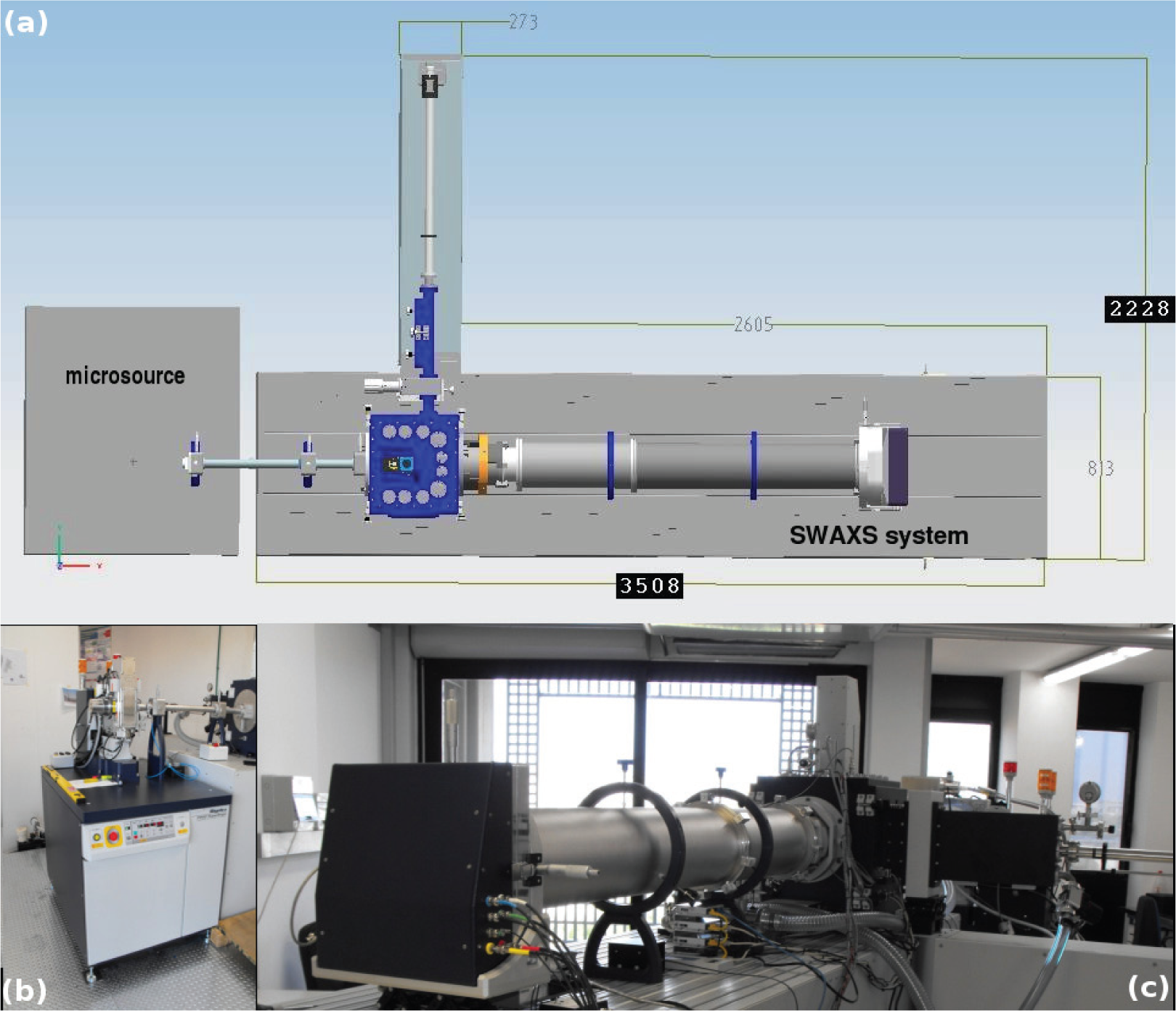
(
The XMI-LAB schematic layout is shown in Figure 7a. The laboratory is equipped with a Fr-E+ SuperBright rotating copper anode micro-source (45 kV/55 mA; Cu-Kα, λ = 0.154 nm, 2475 W), shown in Figure 7b, and a SAXS/WAXS (SWAXS) three pinhole camera (Figure 7c). The X-ray beam is focused through a multilayer focusing optics (Confocal Max-Flux – CMF® 15–105) and collimated by three pinholes, with diameters of 150μm/50μm/200μm (high spatial resolution configuration) or 300μm/150μm/500μm (high flux configuration). The flux measured at the sample position is ~9×10⁶ photons/s in the high flux configuration and the ratio between the flux values in the two configurations is around 34. The system is equipped with two distinct detectors: a Triton™20 gas-filled proportional counter (1024×1024 array, 195μm pixel size) for (GI)SAXS acquisition and an image plate (IP) detector (250×160 mm2 in size, with 50 or 100μm effective pixel size depending upon binning, and an off-line RAXIA reader) to collect (GI)WAXS.
In order to simultaneously measure the SAXS and WAXS images, a 6mm hole is left open in the centre of the Image Plate IP detector. Depending upon the pinhole set, a beam stopper (∅ = 4.0mm; 5.5 mm) is mounted on a holder in front of the SAXS detector, which contains a pin-diode to monitor the beam transmitted through the sample.
The sample detector distance is ~2200 mm for the (GI)SAXS detector and ~28 mm for the (GI)WAXS detector. These distances give access to Q - ranges of about 0.006÷0.2Å−1 for (GI)SAXS and 0.7÷ 4.7Å−1 for (GI)WAXS.
The specimen can be mounted in SAXS/WAXS (transmission) or GISAXS/GIWAXS (reflection) geometry, the latter using a remote-controlled goniometer. The goniometer has a 125×125 mm2 stage with the rotation axes parallel and perpendicular to the primary beam direction, as well as the vertical translation movable by means of three independent stepper piezoelectric motors. The accessible angular range is between -1 and +6 degrees with sub-arcsecond precision.
4. Applications - ex situ studies
4.1 GISAXS – 2D Self-assembly of CdSe/CdS nano-octapods
The accuracy in the determination of size and shape of the building blocks assembled in 1D, 2D or 3D architectures - along with their mutual positions - by GISAXS, is strongly dependent upon the visibility of the interference fringes and, hence, on the signal-to-noise and signal-to-background ratios in the X-ray scattering pattern. The use of synchrotron radiation is often preferable (or even mandatory) because of the weak scattering signal due to the small amount of material in the investigated nanostructured sample. Unfortunately, access to synchrotron radiation instrumentation is traditionally difficult and characterized by long waiting times, and definitely not suitable for in-line routine monitoring, as often required by the synthesis of novel materials. As shown by the research group working at the XMI-Lab of the CNR-IC (Bari), laboratory data quality can be further improved by applying a suitable mathematical treatment (restoration algorithm). If a high brilliance laboratory micro-source (e.g., Rigaku FR-E+ Superbright) is employed for data collection in combination with the algorithm, a final data quality comparable to that of a third generation synchrotron can be achieved. 56 The application of the algorithm allows the deconvolution of the source function (describing the primary beam with its size and divergence) from the measurement and the restoration, at least partially, of missing data cut away by the beam stopper, making hidden features in the GISAXS pattern become visible. For this reason the algorithm has been named ‘RESTORE-DATA’. A suitable test sample was chosen for this study, comprised by octapod-shaped nanocrystals57,58 which have been self-assembled in 2D square lattices on the surface of a silicon substrate. The octapods consist of a CdSe core from which eight CdS pods depart according to an octahedral symmetry. TEM and SEM pictures, together with schemes of the octapods and their assemblies, are reported in Figure 8.

(a) TEM) image of the “unassembled” octapods, deposited on a standard TEM grid. Sketch of an octapod as viewed in two different projections. (b) Sketch of a 2D square lattice of side-to-side aligned octapods, each of them touching the substrate with four pods, as clearly shown by the tilted SEM, inset. In (c) and (d) can be seen SEM images of the actual 2D square lattices of octapods, from the same sample as that shown in (b), at two different magnifications [Reproduced with the permission of the International Union of Crystallography (http://journals.iucr.org/) from L. De Caro, D. Altamura, F. A. Vittoria, G. Carbone, F. Qiao, L. Manna & C. Giannini, “A superbright X-ray laboratory micro-source empowered by a novel restoration algorithm”, J. Appl. Cryst. vol. 45, pp. 869–873, 2012].
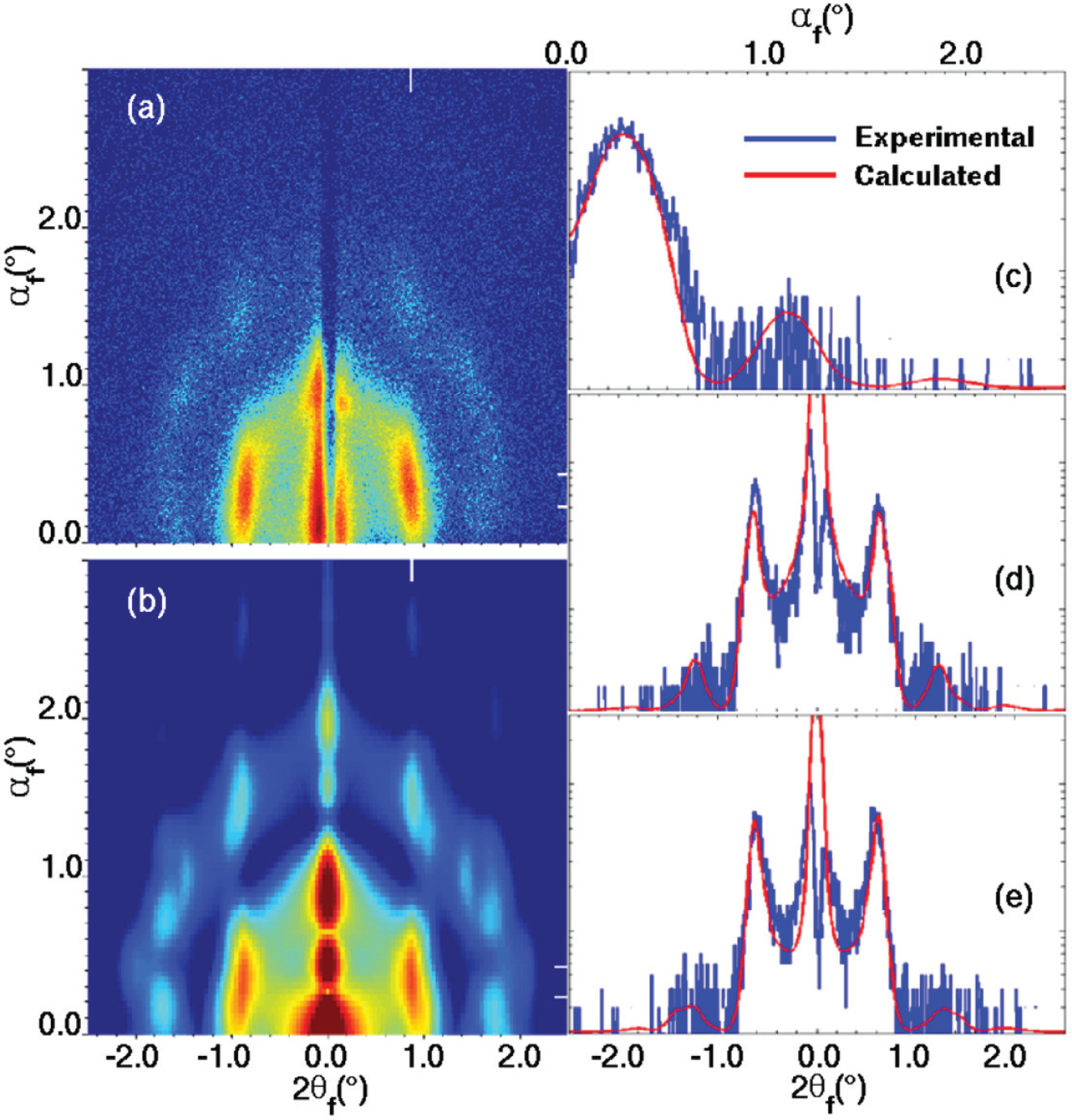
Such a superlattice structure has been analysed through GISAXS for the first time and was chosen as the case study because of the complex shape of the building blocks, which leads to detail-rich characteristic X-ray scattering patterns (see Figure 9).

(a) GISAXS data collected at the ID01 beamline (ESRF) and (b) at the XMI-LAB (IC-CNR); (c) Data in (b) after applying the RESTORE-DATA algorithm. The red square regions marked in panels (a), (b) and (c) are reported in false colours in panels (d), (e) and (f), respectively [Reproduced with the permission of the International Union of Crystallography (http://journals.iucr.org/) from L. De Caro, D. Altamura, F. A. Vittoria, G. Carbone, F. Qiao, L. Manna & C. Giannini, “A superbright X-ray laboratory micro-source empowered by a novel restoration algorithm”, J. Appl. Cryst. vol. 45, pp. 869–873, 2012].
GISAXS data were collected at the ID01 beamline of the European Synchrotron Radiation Facility (ESRF) and at the XMI-LAB (IC-CNR): the raw data are shown in Figures 9a and 9b, respectively. The angle of incidence was 0.13°. Reported in Figure 9c is the 2D GISAXS pattern shown in Figure 9b, after applying the RESTORE-DATA algorithm. A selected area, marked with a red square region for each figure, is zoomed in upon and reported in Figure 9d-f in false colour output, allowing a better appreciation of the differences between the two as collected GISAXS maps and the improved visibility of the features after data restoration (Figure 9c).
Essentially, the RESTORE-DATA algorithm recovers the coherent part Icoh(

Here
As a result, the RESTORE-DATA algorithm leads to a virtual enhancement of the source brilliance, which is responsible for the improvements in Figures 9c and 9f. Such improvements can also be appreciated in the 1D profiles reported in Figure 10, representing the linear cuts taken along the red arrows in panels d-f of Figure 9, which are the kind of dataset generally used in the actual fitting procedure for GISAXS data.

Horizontal cuts extracted along the red arrows in panels d-f of Fig. 9: XMI-LAB raw data (blue line), ESRF-ID01 raw data (red line), restored XMI-LAB data (black line) [Reproduced with the permission of the International Union of Crystallography (http://journals.iucr.org/) from L. De Caro, D. Altamura, F. A. Vittoria, G. Carbone, F. Qiao, L. Manna & C. Giannini, “A superbright X-ray laboratory micro-source empowered by a novel restoration algorithm”, J. Appl. Cryst. vol. 45, pp. 869–873, 2012].
4.2 GISAXS – 3D Self-assembly of iron oxide NCs 59
The bright-field TEM image of ~10 nm iron oxide NCs, shown in Figure 11a, demonstrates the high monodispersity of the NCs, which were used to make millimetre-scale supercrystals, organized as 3D ordered NCs. A guided procedure was used, driving the magnetically responsive NCs organized during slow solvent evaporation from corresponding colloidal solutions under the action of an external applied magnetic field. 60 SEM images, collected at various magnifications, are displayed in Figures 11b-d and show the NCs assembled in a compact film on a substrate, from which several well-separated, distinct 3D conically shaped islands protruded outwards. The inner superlattice organization was revealed by inspecting the island across the sharp ridges visible at such stepped regions and/or in correspondence with induced cracks: regularly stacked NC layers were formed, compatible with cubic- and hexagonal-type structures viewed down the [111] and [001] directions, respectively.

(a) TEM image of the 2D monolayer of NCs on a Cu-supported carbon film of a TEM grid, which had self-assembled upon solvent evaporation; (b-d) Low-resolution SEM images at different magnifications, showing the island-like features on the surface of the NC-built superlattice films; (e-f) High-resolution SEM images of regions within cracks of the islands, where the 3D ordered NC packing can be clearly seen [Reprinted with permission from D. Altamura, V. Holý, D. Siliqi, C.I. Lekshimi, C. Nobile, G. Maruccio, P.D. Cozzoli, L. Fan, F. Gozzo and C. Giannini, “Exploiting GISAXS for the Study of a 3D Ordered Superlattice of Self- Assembled Colloidal Iron Oxide Nanocrystals”, Cryst. Growth Des., vol. 12, pp. 5505–5512, 2012, Copyright (2012) American Chemical Society].
GISAXS data were collected at a very small incidence angle (α i = 0.05deg), as shown in Figure 12a. Indeed, the particular morphology of the sample allowed the measurement of the X-ray intensity scattered from 3D regions of the islands, even with the beam impinging at a highly grazing incidence angle on the substrate.
(a) Experimental and (b) simulated GISAXS maps for 0.05° incidence. Linear cuts along (c) the vertical and (d, e) horizontal directions, through the lines indicated by the white ticks in the maps. The data is simulated using the Born approximation in the LMA description [Reprinted with permission from D. Altamura, V. Holý, D. Siliqi, C.I. Lekshimi, C. Nobile, G. Maruccio, P.D. Cozzoli, L. Fan, F. Gozzo and C. Giannini, “Exploiting GISAXS for the Study of a 3D Ordered Superlattice of Self- Assembled Colloidal Iron Oxide Nanocrystals”, Cryst. Growth Des., vol. 12, pp. 5505–5512, 2012 Copyright (2012) American Chemical Society].
The data were analysed against a new theoretical model 59 (see the calculated map in Figure 12b), as the applicability of software available for the fitting of the whole GISAXS intensity, up to recently, has been either restricted to 2D in-plane assemblies of particles (IsGISAXS), 61 limited to the calculation and indexing of the expected diffraction spot positions (NANOCELL) 62 or devoted to particular types of samples - e.g., with thin film morphology and flat interfaces (NANODIFT). 63
For this study, a new program has been implemented for simulating and fitting GISAXS data collected from compact 3D assemblies. The program is based on a model previously published by Buljan, et al., 64 describing diluted assemblies where the sizes and positions of the quantum dots could be assumed to be statistically uncorrelated. That model was then improved and applied to the GISAXS study of a 3D ordered non-diluted assembly of colloidal iron oxide NCs. Fitting the experimental data (see the calculated and experimental profiles in Figures 12c, d, e) allowed us to determine the fcc-like packing of the superlattice as well as to probe the morphological and size-statistical properties of the assembled NCs. The results were found to be in excellent agreement with information derived by other experimental techniques (SEM and TEM), thus proving that the proposed model was indeed successfully applicable to the study of 3D closed-packed NC assemblies.
4.3 GISAXS/GIWAXS – 3D self-assembly of PbS NCs 52
Among the different IV-VI semiconductor NCs, lead chalcogenide NCs are very appealing because of their emission in the near-infrared region and the strong confinement of charge carriers. In this research field, PbS colloidal nanocrystal assemblies with monomodal and bimodal size distribution have recently been fabricated. 65
An example of GISAXS/GIWAXS studies on the assembly of three-dimensional lead chalcogenide (PbS) nanocrystals (see also the works by Altamura et al., 2012 66 and Corricelli et al., 2011 65 and references therein for details on the chemical synthesis), formed by the slow evaporation of solvent on a Si substrate, is reported below.
Figure 13 shows GIWAXS (upper part) and GISAXS (lower part) data from the same sample region, related to the PbS nanocrystal lattice and the self-assembling superlattice symmetry, respectively. The 1D profiles reported in Figures 13b and 13d are obtained through the azimuthal integration of the corresponding Figures 13a and 13c. These profiles reveal the rock-salt (CsSl-type) cubic structure of the PbS nanocrystals (about 2 nm in diameter, as determined by the red superimposed fitted line) and a body-centred cubic superlattice. 67

Data collected from an assembly of 2 nm PbS nanocrystals: (a) GIWAXS; (b) 1D pattern extracted from (a); (c) 2D GISAXS image; (d) 1D GISAXS profile [Reproduced with the permission of the International Union of Crystallography (http://journals.iucr.org/) from D. Altamura, R. Lassandro, F. A. Vittoria, L. De Caro, D. Siliqi, M. Ladisa and C. Giannini, “X-ray micro-imaging laboratory (XMI-LAB)”, Journal of Applied Crystallography, vol. 45 (4), 869–873, 2012].
4.4 GIWAXS – Organic field effect transistors based on poly(3-hexylthiophene) 68
Nanofibres of regioregular poly(3-hexylthiophene) (P3HT) were fabricated by solvent-resistant nanolithography and used as the active medium in organic field effect transistors (OFET). 68 This process favoured a remarkable improvement of the device performance because of the nanofluidic flow in perfluoropolyether capillaries and the slow solvent evaporation rate in the mould cavities, which induced the reorganization of the P3HT chains and allowed us to obtain a charge carrier mobility 60 times higher than in the corresponding homogenous films. GIWAXS 2D patterns were collected and are shown in Figure 14 for OFET with 270 nm wide features, obtained by polydimethylsiloxane (PDMS) (a), by perfluoropolyether (PFPE) moulds (b), and for 80 nm wide features by PFPE moulds (c). Self-organization in P3HT resulted in a lamellar structure with two-dimensional conjugated sheets formed by inter-chain stacking, leading to (100) reflections due to the layer lamellar structure and (010) reflections due to π–π inter-chain stacking. Orientations of P3HT crystallites with respect to the substrate were identified from the different intensity distributions of (100) and (010) reflections. The sequence of schematics from left to right in Figure 14(e) represents GIWAXS 2D patterns together with the relevant lamellar structures oriented mostly parallel to the substrate surface (face-on), predominantly perpendicular to the substrate surface (edge-on) and randomly with respect to the substrate surface, respectively. Therefore, Figures 14a-c show that the preferential orientation of the P3HT ordered domains is with the (100)-axis normal to the film and the (010)-axis in the plane of the film (edge-on orientation). 69

GIWAXS analysis of the realized P3HT nanostructures. 2D patterns of 270 nm wide features obtained by a PDMS mould (a) and a PFPE mould (b), with 80 nm wide features realized by a PFPE mould (c) [Reproduced by permission of The Royal Society of Chemistry from E. Mele, F. Lezzi, A. Polini, D. Altamura, C. Giannini, and D. Pisignano, “Enhanced charge-carrier mobility in polymer nanofibers realized by solvent-resistant soft nanolithography” J. Mater. Chem., vol. 22, pp. 18051–18056, 2012 (http://pubs.rsc.org/En/content/articlelanding/2012/jm/c2jm33611a)]; geometry of the measurement (d) [Reprinted from http://repository.lib.ncsu.edu/ir/handle/1840.16/7766]; orientation of the lamellar structures with respect to the substrate surface (e) [Reprinted with permission from D. J. Herman, J. E. Goldberger, S. Chao, D. T. Martin and S. I. Stupp, “Orienting Periodic Organic/Inorganic Nano-scale Domains Through One-Step Electrodeposition” ACS Nano, 2011, 5, 565–573. Copyrigth (2011) American Chemical Society].
The lattice parameters a (the distance between the backbones) and b (π-stacking distance) ≅ c/2 (separation between the side chains) were derived from the out-of-plane (along Qz) and in-plane (along Qr) radial cuts extracted from the 2D GIWAXS maps, and are approximately (1.67 ± 0.03) nm and (0.38 ± 0.02) nm, respectively, as is typical of ordered P3HT. 70
5. Applications - in situ studies
GISAXS can also be applied in situ for the real-time monitoring of the nanoparticles assembly and growth, allowing for the study of the kinetic processes and the temporal correlations of structural parameters such as array size, shape and spatial distribution, which are fundamental for tuning the physical properties of the systems. The use of the synchrotron radiation is needed to analyse several evaporation stages, performing GISAXS experiments with a suitable time resolution. A few selected examples are described in what follows, although many others can be found in the literature (see, e.g., refs.71–73).
5.1 In situ GISAXS – Dynamic investigation of gold nanocrystal assembly 74
In this work, stable aqueous solutions of monodisperse gold NCs were synthesized according to the preparation route developed by Brust et al. 75 and followed by heat treatment in order to narrow the size distribution (~7%). A micro-emulsion process driven by interfacial tension was used to encapsulate NCs within micelles of cetyltrimethylammonium bromide (CTAB). The final solution was highly stable, with a concentration of Au NCs in water of ~50 mg/mL. For self-assembly into a silica matrix, 0.08 mL of tetraethyl orthosilicate was added to 1 mL of Au NC solution, along with 0.05 mL of 0.07N HCl catalyst. For the in situ scattering studies presented here, this solution was further diluted by a factor of 10.
The dynamic self-assembly of pathway of ordered gold nanocrystal arrays, during the self assembly of gold nanocrystal micelles, has been investigated by performing in situ GISAXS at a synchrotron beamline with and without the presence of colloidal silica precursors. Scattering data were obtained every 120 s with an integration time of 30s. Figure 15 shows GISAXS data from the self-assembly of Au NC micelles with (A,B), the corresponding evolution of unit cell parameters over time (C), and without (D, E,F) the presence of silica precursors at different times.

GISAXS data from the self-assembly of Au NC micelles with (A-C) and without (E,F) silica precursors. (C) Evolution of unit cell parameters (space group R m) over time. (D) An intermediate layer observed in the Au-NC-micelle (no silica). The incidence angle is 0.2° [Reprinted with permission from D. Dunphy, H. Fan, X. Li, J. Wang, and C.J. Brinker, “Dynamic Investigation of Gold Nanocrystal Assembly Using In Situ Grazing-Incidence Small-Angle X-ray Scattering”, Langmuir, vol. 24, pp. 10575–10578, 2008, Copyright (2008), American Chemical Society].
In situ experiments suggest a mechanism of self-assembly whereby lattice formation is driven by the bulk concentration of Au-NCs during solvent evaporation. The preferential orientation is probably induced by confinement between the liquid/solid and liquid/air interfaces. Different behaviour in relation to the domain orientations has been observed during the slow evaporation of the solvent and rapid kinetics in spin-coated films. Moreover, the self-assembly of Au-NCs is observed without the presence of silica, confirming that this process is driven by a long-range (non-specific) force. Indeed, the addition of silica precursors (along with acid catalyst) modifies the self-assembly pathway in a manner consistent with Coulomb screening rather than specific close-range interactions. Without silica, the Au NC lattice collapses upon the completion of the solvent's evaporation.
5.2 In situ GISAXS – Self-assembly of iron oxide nanoparticles 76
The iron oxide nanoparticles were synthesized through a high temperature solution phase reaction of metal acetylacetonates (Fe(acac)3) with 1,2-hexadecanediol, oleic acid and oleylamine in phenyl ether using toluene as a solvent. 77 The nanoparticles are of a single domain and behave as single bipoles due to the weak dipole-dipole interaction of magnetic iron oxide nanoparticles. They also present a crystalline structure and superparamagnetic properties at room temperature. The drops of colloidal solution were deposited onto silicon substrates of 1cm 2 covered with a native SiO2 layer. Monolayers of the iron oxide nanoparticles were prepared through solvent evaporation from the drop of the colloidal solution, applied on the substrate at room temperature, following three different stages of drying.
The self-assembly of the colloidal nanoparticles was studied through time-resolved GISAXS measurements using both synchrotron radiation and a conventional X-ray rotating anode source, both in the substrate and drop modes.
Three typical stages of the temporal evolution in the substrate mode and the drop mode are shown in Figure 16 (a-c-e) using the t-q y intensity maps, in which the intensity corresponding to a particular (t, q y ) point is obtained by an integration of the measured intensity over the q z interval at a constant q y in the GISAXS pattern. Moreover, in order to quantify the temporal evolution, the scattered intensity has also been integrated over the q y interval to obtain a partial integrated scattering (PIS) as a function of time.

A t-q y map of a drying colloidal drop forming ordered (a) monolayer, (c) sub-monolayer arrays of nanoparticles measured in the substrate mode and in (e) drop mode; the corresponding (b-d-f) partial integrated scattering (PIS) plot [Reprinted with permission from P. Siffalovic, E. Majkova, L. Chitu, M. Jergel, S. Luby, A. Satka, S.V. Roth, “Self assembly of iron oxide nanoparticles studied by time resolved grazing incidence small angle X ray scattering”, Physical Review B, vol. 76, pp. 195432-8, 2007 Copyright (2007) by The American Physical Society].
During the synchrotron measurements, the contributions of the volume and surface X-ray scattering were separated during self-assembly. The focused X-ray beam provided the temporal evolution of the volume and surface scattering from the drop, being undisturbed by the substrate scattering and, thus, giving an insight into possible nanoparticle self-assemblies forming inside or on top of the drop surface. At a distance from the surface larger than 80 μm, the colloidal solution shows the absence of self-assembled clusters in the drop volume or self-assembled domains on the drop surface, such that we can assume that the self-assembly takes place near the three-phase (solid/liquid/vapour) drop contact line as the solvent evaporates.
Similar measurements with a better temporal resolution have been performed with an x-ray rotating anode, enabling to also monitor the early stage of the self-assembling process. Moreover, fast transients of the GISAXS in the final evaporation stage have been observed - as shown in Figure 17 - indicating the highly nonlinear behaviour of the volume and surface X-ray scattering, due to the evaporation-driven surface tension instabilities of the drying drop.

Partial integrated scattering plot of a drying colloidal drop in the substrate mode, measured with an X-ray anode source [Reprinted with permission from P. Siffalovic, E. Majkova, L. Chitu, M. Jergel, S. Luby, A. Satka, S.V. Roth, “Self assembly of iron oxide nanoparticles studied by time resolved grazing incidence small angle X ray scattering”, Physical Review B, vol. 76, pp. 195432-8, 2007 Copyright (2007) by The American Physical Society].
5.3 In situ GISAXS - Semiconductor nanorod self-assembly at the liquid/interface 78
The self-assembly of colloidal CdSe/CdS nanorods (NRs) at the liquid/air interface was studied by combining time-resolved in situ GISAXS and ex situ Fast Fourier Transform TEM (FFT-TEM). The method 79 used for the chemical synthesis of CdSe/CdS dot core/rod shell NRs, allows for control over the length of the NRs by tuning the CdSe seed concentration and by adjusting the temperature and reaction time. The process of the NRs' self-assembly was studied by in situ GISAXS on three different bathes of NRs with variable narrow size distribution so as to follows the dynamics of NR self-assembly (long NRs with length L = (48 ± 4) nm and diameter 2R = (4.1 ± 0.4) nm, (ii) medium-length NR with L = (22.2 ± 2.3) nm and 2R = (6.3 ± 1.0) nm, and (iii) short NRs with L = (16.3 ± 2.4) nm and 2R = (3.4 ± 0.3) nm). The experiment was performed at a synchrotron beamline with an incident X-ray energy of 13.3 KeV at a grazing incidence angle of α i = 0.061° so that the beam only probes the toluene/air interface at most 10/20 nm deep into the NRs dispersion.
Through in situ GISAXS patterns, it is possible to follow the dynamics of the self-assembly and study the formation of large areas of vertically- and horizontally-aligned nanorods (NRs) at the liquid/air interface obtained by controlling solvent evaporation, as shown in Figure 18 for medium-length NRs.

GISAXS patterns of the superstructures of medium-length NRs (L = 22 nm) at the liquid/air interface, at different stages after the beginning of solvent evaporation: (a) 12 min, (b) 14 min, and (c) 16 min. Colour scales are logarithmic. Scale bars are 0.5 nm−1. (d, e) Schematics of the NRs' structures as present (d) at the beginning and (e) at the end of the self-assembly process [Reprinted with permission from F. Pietra, F.T. Rabouw, W.H. Evers, D.V. Byelov, A. Petoukhov, C. de Mello Donegá, and D. Vanmaekelbergh, “Semiconductor nanorod self-assembly at the liquid/air interface studied by in-situ GISAXS and ex-situ TEM”, Nano Lett., Just Accepted Manuscript, 2012, Publication Date (Web): 05 Oct 2012 Copyright (2012) American Chemical Society].
By this method, it is possible to prove that the NRs' superstructure occurs at the liquid/air interface and partly follow the dynamics of self-organization. The NR length and the initial concentration in the NR dispersion are able to tune the orientation of the NRs in the final superstructure, thus allowing the construction of a model of hierarchical self-organization that accounts for the NR length and concentration dependence of the superstructures formed.
5.4 In situ GISAXS - Flat-top silver nanocrystals on the two polar faces of ZnO 80
In this work, an in situ GISAXS technique was used to study the growth of silver at room temperature on two polar (000&1macr;)-O and (0001)-Zn surfaces of ZnO. The ZnO substrates were hydrothermally grown as single crystals with (0001) and (000&1macr;) orientations. The clean surfaces were obtained after several cycles of sputtering with Ar+ and annealing at high temperature in UHV, followed by cooling down under O2 pressure. The silver was evaporated using a heated Knudsen cell, the substrate being kept at room temperature. The amount of Ag/ZnO films deposited, expressed in nanometres, can be determined by using a calibrated flux of silver, measured with a quartz microbalance.
Figure 19 shows some experimental GISAXS patterns recorded during the growth of Ag on the Zn and O surfaces, indicating a decrease of the distance between the two intensity lobes with increasing coverage.

In situ GISAXS measurements during Ag depositing on the ZnO(0001) Zu-terminated surface (left column) and on the ZnO(000&1macr;) O-terminated one (right column) [Reprinted with permission from N. Jedrecy, G. Renaud, R. Lazzari, and J. Pupille, “Flat-top silver nanocrystals on the two polar faces of ZnO: an all angle x-ray scattering investigation”, Physical Review B, vol. 72, pp. 045430, 2005 Copyright (2005) by The American Physical Society].
The results show that on both polar surfaces of ZnO, silver forms nanoclusters assembled with well-defined top facets, in (111) epitaxy with [10&1macr;]Ag||[100]ZnO.
In situ and quasi-real-time GISAXS allows a precise understanding of the metal/oxide interface structure, both in the nanoscopic and mesoscopic scale, with significant differences in the morphology of the films. In particular, the GISAXS data shows a triangular development of Ag nanoclusters on the Zn face, whereas the O face leads to a hexagonal one.
Quantitative analyses have been performed to deduce the morphological parameters as a function of coverage. The Ag films at high coverage were modelled by continuous layers with holes in it: in the case of O, flat-top islands develop mostly laterally until an incompletely filled thick layer is formed; in this case, the GISAXS data are well represented by using an island model instead of hole model. In the Zn case, a mixture of clusters and holes with similar shapes and in close proportion is inferred.
The derived growth parameters attest that silver spreads significantly better on the O-terminated face than on the Zn termination.
6. Summary and perspectives
Nanoscale architectures can be produced with ‘top-down’ (physical methods) and with ‘bottom-up’ approaches (physical/chemical methods).
This chapter provides basic notions as to Grazing Incidence Small Angle X-ray Scattering (GISAXS), a technique typically used to study nanostructured surfaces. A few relevant examples of in situ and ex situ experiments performed on assembled nanostructured architectures synthesized with chemical synthesis approaches are provided. Additionally, some applications of Grazing Incidence Wide Angle X-ray Scattering (GIWAXS) are also given.
At present, different types of nanoscale architectures, embedded in planar devices, provide very interesting possibilities in nanomedicine, being aimed at identifying biological species without the need for fluorescent or radiological pre-labelling. 81 In perspective, GISAXS/GIWAXS each offer very promising opportunities in this context, allowing for the ex situ and in situ study of the device characteristics in real-time and providing important information on how to achieve target molecules' quantification, improving devices' sensitivity and capacity for the high throughput screening of biological samples.
Footnotes
7. Acknowledgements
The authors would like to thank the SEED project “X-ray synchrotron class rotating anode micro-source for the structural micro imaging of nanomaterials and engineered bio-tissues (XMI-LAB)”- IIT Protocol n.21537 of 23/12/2009 and the FIRB 2009/2010 project “Rete integrata per la Nano Medicina (RINAME)” –RBAP114AMK_006. Rocco Lassandro is acknowledged for the technical support given in the XMI-LAB.