
Abstract
Interfacial microstructures between thick Al wires and pads formed by ultrasonic bonding were analysed to investigate the behaviour of bond preventing phases. The wire and the substrate form direct bond interface in the central region of the bond area, whereas the surfaces of them in the peripheral region are covered by amorphous Al2O3 bond preventing layer. The amorphous Al2O3 layer is chipped off the surfaces by application of ultrasonic vibration and forms a number of spherical particles intervening between the wire and the substrate. The particles consist of amorphous Al2O3 matrix and lamellae of Al. The particles grow by accumulating the amorphous Al2O3 on the surfaces of the wire and the substrate in contact, moving outward the bond area. The bond area expands through the area where the bond preventing layer has been removed.
Keywords
Introduction
Power electronics has been a technology to transform electric power and to manage power flow in electric and electronic appliances. Recently, to improve energy efficiency of the appliances has become one of its most important roles. In the near future, it will be the key technology for establishing dispersed renewable power systems.1 Application of power electronics is extending to those demanding high power capability, high energy efficiency and long service life.2 Thus, the demands are getting severer. In addition, all power electronic devices have to guarantee extremely high reliability, since only one failure can halt the entire system. The wire bonds interconnecting the power electronic devices with outer circuits also have to satisfy the requirements. Generally, thick high purity aluminium wires are bonded using ultrasonic bonding technique to interconnect power electronic devices with outer circuits.3 In order to satisfy the severe requirements, the bonding process requires optimised control based on the firm knowledge of the bonding mechanism and the interfacial microstructure evolving during the process.
Takahashi et al. have studied the deformation of wires and pads during thermocompression bonding by finite element numerical analysis.4, 5 Their results clarified the expansion behaviour of the bonded area, which can be adopted also to ultrasonic bonding. Seppänen et al. proposed a two-stage mechanism to explain the interfacial phenomena during ultrasonic bonding, namely, the slip and fold mechanism.6 In the slipping stage, bond preventing layers are removed from both bonding surfaces by scrubbing the surfaces with each other. Contacting surfaces, being free of bond preventing layers, immediately adhere to each other and form initial bond areas. Then, the bonding proceeds to the folding stage, in which the bond areas expand by folding the side surfaces of the wire onto the substrate. The folding deformation also exposes fresh surface, which is free of bond preventing layers, to the bond interface and helps the bond formation.
On the other hand, the evolution of interfacial microstructure is still not clearly understood. Krzanowski and Murdeshwar have studied the interfacial microstructure of ultrasonic bonds between Al wires and substrates in detail by transmission electron microscopy.7 Their results have proven the formation of dynamically recrystallised interfacial microstructure. Furthermore, they have shown a method to estimate the thermal effect of the ultrasonic bonding by measuring the width of dislocation loop free zone in the vicinity of grain boundaries, which indicated that the effect is equivalent to annealing at 250°C for 90 ms. Lum et al. have investigated the evolution of bond footprints left on the substrates after shear test of the bonds.3 Their results showed clearly that the interfacial sliding behaviour changes between microslip and gross sliding depending on the combination of bonding force and ultrasonic power. However, the interfacial microstructure at the bond periphery, i.e. the front line of the bond formation, has not been reported so far. To know how bond area expands, standing on experimental analysis of the interfacial microstructure is important for designing the bonding variables and for supporting the abovementioned slip and fold mechanism.
The present study aims to analyse interfacial microstructure formed by ultrasonic bonding, placing the emphasis on the structure and distribution of Al2O3, the representative substance of the bond preventing layer on Al surface. Based on the analysis results, the interfacial phenomena including the behaviour of Al2O3 during ultrasonic bonding are discussed.
Experimental
The wire material used in the present study was pure Al of which diameter and nominal purity were 300 μm and 99·9% respectively. On the other hand, two types of substrate materials were employed. One was a 1·00 mm thick Si single crystal wafer with the surface of (100) plane (bare–Si substrate), and the other was a 1·5 μm thick Al–1 mass-%Si alloy film deposited on 0·6 mm thick Si (100) wafer with 0·5 μm thick oxide layer (Al padded substrate). The Al–Si alloy film was deposited by electron beam deposition. The substrates were cut into squares of 5·0 mm on a side for use in each experiment. The wires and substrates were degreased by ultrasonic cleaning in acetone just before the bonding process.
Ultrasonic bonding of the wires to the substrates was implemented under a fixed ultrasonic frequency of 110 kHz without external heating. Although this frequency is higher than those generally used in electronics packaging, it is known that higher frequency enhances the bondability and allows bonding under low ultrasonic power suppressing damage introduction to the bonds.8 To avoid such damage is preferred for the analysis of the bonding mechanism, since the damage is formed after bonding is once achieved. The process parameters consisting of bonding force F, ultrasonic power P and applying time of ultrasonic vibration t were set to 3·5 N, 1·0 W and 200 ms respectively, which were determined by the preliminary investigation to find preferable bonding condition at which the bonding proceeds through the slip and fold mechanism. The wedge tool used in the present study was made of cemented carbide and had a U grooved chucking tip. The wire was laid on the substrate, pressed on the substrate with the wedge tool, and then ultrasonic vibration was applied to the direction parallel to the wire axis.
Some of the interfaces were analysed from the cross-section at the centre of the bond area, and the other were analysed from plan view section after removing the Al wire by immersing carefully in hydrochloric acid aqueous solution to retain the Al2O3 residue particles on the substrates. Scanning electron microscopy (SEM), electron probe microanalysis (EPMA) and transmission electron microscopy (TEM) were used to analyse the interfacial microstructures. The SEM and EPMA samples were embedded in resin and then ground and polished. The TEM samples were prepared by focused ion beam microsampling technique.
Results
Figure 1 shows cross-sectional SEM images of an interface between Al wire and Al padded substrate bonded under the condition of F = 3·5 N, P = 1·0 W and t = 200 ms. The profile of Al wire shown in Fig. 1a indicates that the width of the area slid on the substrate is 322 μm, which is almost the same with the wire diameter. However, not the entire slid area forms bond. In the central region of the interface shown in Fig. 1b, the wire fays the substrate. On the other hand, the wire is lifted off the substrate in the peripheral region as shown in Fig. 1c. The width of the actual bonded area at this cross-section is 226 μm.
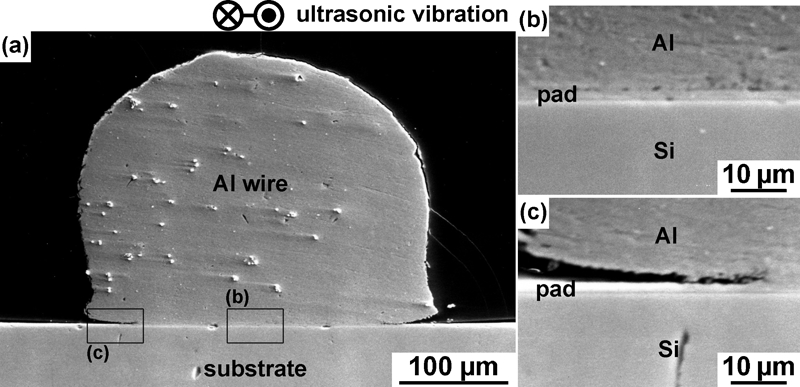
Cross-sectional SEM images of interface formed by ultrasonic bonding under bonding condition of F = 3·5 N, P = 1·0 W and t = 200 ms
If the bonding is carried out without applying ultrasonic vibration, i.e. by only pressing the wire on the substrate with the static bonding force of 3·5 N, it fails. In addition, the wire is not plastically deformed to form wide faying interface. Thus, the formation of wide bond area observed in Fig. 1a is considered to be induced by application of ultrasonic vibration.
The microstructure at the edge of the bond area in the peripheral region was analysed by TEM and compared with that at firmly bonded interface in the central region. Figure 2 shows bright field TEM images of the central and peripheral regions sampled from the interface shown in Fig. 1. The interface of the central region depicted in Fig. 2a indicates that the wire and the substrate are bonded directly. Phases corresponding to bond preventing layers are scarcely observed in the vicinity of the interface. The microstructure of the wire beside the interface consists of submicrometre sized equiaxial grains, whereas the wire matrix consists of micrometre sized grains elongated towards the wire axis. This result indicates that recrystallisation has occurred during ultrasonic bonding, which is consistent with the report by Krzanowski and Murdeshwar.7 On the other hand, the interface of the peripheral region depicted in Fig. 2b appears different from that of the central region. A gap (partially filled with fixing resin) is observed between the wire and substrate, indicating that the bond is not achieved in this region. In the gap, spherical particles (although the largest particle in Fig. 2b appears levitating in the gap, it is considered to be in contact with surfaces of the wire and the substrate somewhere in a different cross-section) are observed with monotonous greyish contrast. The size of the particles varies from 0·2 to 1·6 μm. In addition, the surfaces of the Al wire and the Al–1 mass-%Si pad are also covered by the same greyish phase. Since this greyish phase is not observed in the bond interface of the central region, it is considered that the phase interferes the bond formation.
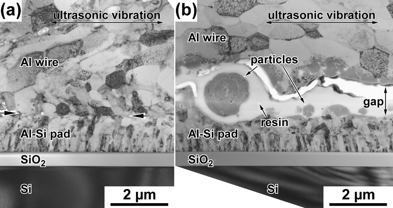
Bright field micrographs of interface bonded under condition of F = 3·5 N, P = 1·0 W and t = 200 ms: arrows in a indicate bond interface
The microstructure of the largest particle observed in Fig. 2b was analysed further. Figure 3a shows a magnified bright field image of the particle. In addition to the greyish matrix (marked as ‘M’ in the figure) of the particle, dark contrasted fine grains ‘P’ and bright contrasted concentric lamellae ‘L’ are observed. Figure 3b shows the selected area electron diffraction pattern corresponding to the area encircled with white dashed line in Fig. 3a. The pattern consists of Debye–Scherrer rings of Al and halo rings of an amorphous phase. Dark field observation revealed that the dark grains and the bright lamellae are both Al and the matrix is amorphous. The composition of the amorphous matrix analysed by EPMA is Al–63 at-%O, which agrees with that of Al2O3. The greyish phase covering the surfaces of the wire and the substrate shown in Fig. 2b is also considered as the same amorphous Al2O3.
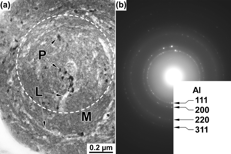
Detailed analysis of largest spherical particle observed in Fig. 2b
In order to investigate the distribution of the particles in the interface, an Al wire was bonded to a bare–Si substrate under the condition of F = 3·5 N, P = 1·0 W and t = 200 ms, and then Al was selectively dissolved in hydrochloric acid. This treatment retains amorphous Al2O3 particles on the bare Si substrate. Figure 4 shows plan view SEM images of the interface after removal of the Al wire. Figure 4a depicts the whole bond imprint of the interface. The central region of the bond area appears in a similar contrast with that of the bare Si substrate. In the magnified micrograph of this region shown in Fig. 4b, fine particles with bright contrast are sparsely observed. These particles correspond to the amorphous Al2O3 particles shown in Fig. 3. The particles would have been trapped in the expanding bond area during bonding. On the other hand, the peripheral region of the interface appears with bright contrast surrounding the bond area. The contrast becomes obvious in the toe and the heel parts, whereas it is obscure in the side edges of the bond area. The magnified micrograph of the heel part in the peripheral region shown in Fig. 4c indicates that the bright contrast corresponds to thickly agglomerated amorphous Al2O3 particles. Sizes of the individual particles in the peripheral region are <2 μm, which are almost the same with those in the central region.
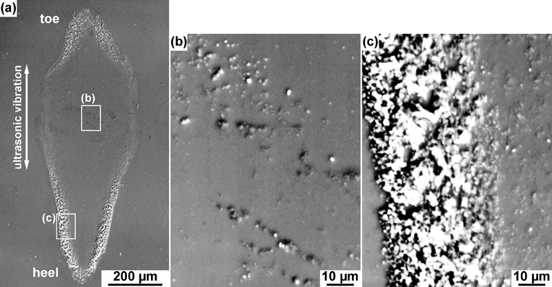
Typical appearance of ultrasonic bond imprint on bare–Si substrate after removal of Al wire by hydrochloric acid: bonding condition was F = 3·5 N, P = 1·0 W and t = 200 ms
Discussion
Al is known to form stable and firm passivation layer of Al2O3 on its surface, which protects Al from further oxidation.9 It is natural to consider that the Al wires used in the present study are covered by thin Al2O3 film in the initial state. However, the amorphous Al2O3 bond preventing layer shown in Fig. 2 appears considerably thick. The layer should have grown during ultrasonic bonding. Although heat generated by ultrasonic friction raises the temperature at the interface,10 it is hardly considered that the oxidation is enhanced solely by the frictional heat: thermal oxidation of solid Al surface does not proceed so rapidly to reach 700 nm within 200 ms.9 Consequently, a consideration is needed to understand the interfacial phenomena during ultrasonic bonding from the results of the present study. In the following text, the origin and the behaviour of the bond preventing phase during ultrasonic bonding are discussed.
The microstructure of the amorphous Al2O3 particle shown in Fig. 3 provides an insight about the formation and growth of the particle. At first, amorphous Al2O3 covering the surfaces of the wire and substrate is chipped off by ultrasonic scrub motion of the surfaces. Then, it rolls between the surfaces of the wire and substrate accumulating amorphous Al2O3 on the surfaces in contact involving small amount of Al like a snowball. Since amorphous Al2O3 also prevents itself from bonding, the growth of the particles will need small amount of Al as the binder. The ultrasonic scrub motion of the surfaces and the gradual folding deformation of the wire will determine the rolling direction of the particles outward the bond area, i.e. the particles are exhausted from the interface. On the other hand, the bond area expands through the area where the bond preventing layer has been removed.
Then, it should be clarified whether the amorphous Al2O3 particles move a long distance from the initial contact area at the centre to the periphery of the final bond area. Since the particles grow by accumulating the amorphous Al2O3 on their moving path, the particles in the peripheral region should have grown larger than those trapped in the central region. However, the results shown in Fig. 4 indicate that the particle sizes in both regions are similar. Furthermore, the thickness of the layer being up to 700 nm as shown in Fig. 2b and the size of the particles being <2 μm indicate that the particles have moved only a short distance, i.e. the particles are formed in the vicinity of the place they are observed. Therefore, the oxidation is considered to have been enhanced locally in the peripheral region.
It should be noted that the wire and the substrate in peripheral region of the bond area are not in contact at the initial state of bonding. Their contact interface expands gradually by folding the side surfaces of the wire. This fact indicates that the enhancement of oxidation does not occur at the early stage of ultrasonic bonding.
Another aspect of the behaviour of the amorphous Al2O3 particles observed in Fig. 4 is that the particles agglomerate significantly in the toe and the heel parts compared to the side edges. In the toe and the heel parts, the wire and the substrate suffer large alternating tensile and compressive deformation due to the constraint by the bond area.11, 12 In addition, a rotational moment to lift off the wire from the substrate acts on the backside of ultrasonic motion corresponding to either of these parts.11 The deformation breaks the passivation layer on Al and exposes fresh Al to the interface. Although the fresh Al can form bond immediately when it meets activated surface on the counter side, it is also easily oxidised if it fails to form bond within a cycle of the ultrasonic motion. To form bond gets difficult by increasing the size and number of the amorphous Al2O3 particles in the vicinity of the fresh Al, i.e. the probability for the fresh Al to be oxidised will increase by proceeding of the ultrasonic bonding. On the other hand, the side edges of the peripheral region are deformed in shear mode. The rotational moment to lift off the wire from the substrate is negligibly low. Although shear deformation can break the passivation layer, fresh Al surface is not exposed effectively by the deformation. Thus, the oxidation in this part is not enhanced obviously.
Thus, ultrasonic bonding is considered to proceed as follows. In the early stage, initial oxide films on the wire and the substrate are broken and pelt off by ultrasonic scrubbing. Since the films are thin, the particles are fine and have negligible effect on hindering bond formation. Bonds will be easily formed and oxidation will not be enhanced. After the initial bond is formed, the ultrasonic relative motion is suppressed by the constraint of the bond. The stress arisen in the vicinity of the bond deforms the wire to fold on the substrate. The area in contact increases by the deformation. The particles move outward the interface, removing the oxide films from the surfaces of the wire and the substrate. This phenomenon enhances the bond area expansion at first. However, the particles grow larger by moving through the interface. Expansion of the bond area gets gradually suppressed by increasing the size and number of the particles. Failure in bond formation enhances the oxidation of the surfaces. Finally, the particles grown up to ∼2 μm prevent further expansion of the bond area and agglomerate in the vicinity of the bond area.
Conclusions
Ultrasonic bonding of thick Al wires to Al padded and bare Si substrates was implemented. The interfacial microstructure was analysed by SEM, EPMA and TEM emphasising on the structure and distribution of Al2O3. The following points are clarified.
Thick Al wires cannot be bonded in the ambient atmosphere and temperature without applying ultrasonic vibration.
In the central region of the bond area, direct bond interface is formed. The bond preventing particles, consisting of amorphous Al2O3 and small amount of Al, exist sparsely in this region.
In the peripheral region of the interface where bond is not achieved, a considerable amount of the particles intervene between the wire and the substrate. The surfaces of the wire and the substrate are also covered by amorphous Al2O3. The particles agglomerate thickly especially in the toe and the heel parts of the peripheral region.
The bond preventing particles grow by accumulating the amorphous Al2O3 on the surfaces of the wire and the substrate in contact, moving outward the bond area. The bond area expands through the area where the bond preventing layer has been removed.
Footnotes
Acknowledgements
The authors express their gratitude to Professor Emeritus H. Mori and Mr E. Taguchi for their kind permission and assistance to use facilities in the Research Center for Ultra-High Voltage Electron Microscopy, Osaka University. Support from the Japan Society for Promotion of Science through Grants-in-Aid for Scientific Research (grant no. 18206076) is also acknowledged.
This paper is part of a special issue from Eco-Mates 2011