
Abstract
The emphasis of this paper lies in the fabrication of a three-layer polydimethylsiloxane chip for micro liquid sample operation. In this paper, the microchannels with a rectangular control layer cross section are fabricated based on a dry-film negative photoresist mold, while the microchannels with a rounded liquid layer cross section are fabricated by a positive photoresist reflow mold. The relationships between temperature and the time of reflow and the arc level of the liquid layer mold are discussed. Different ratios, curing temperatures, and curing times are used to fabricate the two PDMS layers to improve their toughness and plasticity separately. The PDMS slabs with microstructure networks are treated with oxygen plasma to improve their surface properties. The improved surface properties serve to reduce the temperature and time, and improve the sealing strength, which is as effective as adding PDMS in varying ratios. The micro liquid sample operation experiments show that high levels of pinching off and mixing performances on pneumatic microfluidic chips are obtained more easily.
Introduction
The microfluidic technique has attracted increasingly wide attention and become a hot topic in recent years. Pneumatic microfluidic chips have emerged as attractive techniques for biological and chemical applications, primarily due to their advantages, such as high separation efficiency, low reagent consumption, and potential portability.1–3 Polymer-based microfluidic chips have gained more interest because they have a number of advantages over quartz, silica, and glass-based microchips.4,5 The pneumatic microfluidic chips were preferably applied in elastic polydimethylsiloxane (PDMS) material, due to the key merits of the PDMS material, such as its transparency, remarkable mechanical behavior, simple structure bonding process, and low production cost. 6 In particular, the smaller Young’s modulus value of PDMS compared with that of other hard materials has enabled us to use it as the deformable membrane of pneumatic microfluidic devices, which is crucial for the pneumatic microvalves, micropumps, micromixers, and so forth.7–9
Traditional microfluidic chips consisted of two layers, a cover plate and a substrate plate. A cover plate was bonded onto the substrate plate to construct sealed microchannel networks. 10 However, the bulky volumes of the actuators for active functions, such as on-chip microvalves and micromixers, had to be embedded in the fluidic chips, and definitely affected the degree of microfluidic large-scale integration (mLSI). 11 Compared with the two-layer microfluidic chips, multilayer (more than three layers) microfluidic chips have shown the advantage of achieving better performances in reducing chip size and have become a hot topic in microfluidic fields.12,13 However, the multilayer microfluidic chips reported were always fabricated by complicated, costly, and time-consuming processes, and the reliability and portability of these devices were always not good. 14 For the three-layer PDMS pneumatic microfluidic chips, their control systems and pressure generation were usually off chips. Therefore, it became possible to develop a microfluidic chip with thousands of integrated microvalves, micromixers, and other micro components. Such microfluidic chips, including a high density of pneumatic microvalves and micromixers, were developed for parallel high-throughput screening of fluorescence-based single-cell assays. 15 The microchannels on the control layer and liquid layer were fabricated by several methods, such as hot embossing, 16 laser fabrication, 17 reactive ion etching, 18 electroforming, 19 and soft lithography. 20 The two layers were separated by an elastic PDMS thin membrane, which could be obtained from spin coating by controlling the equipment speed. The soft lithography method involving thick-film micromachining and replica molding of PDMS materials has become popular and is promising in applications due to its rapid and reliable fabrication. However, none of the current techniques allow for a possible combination of a simple out-of-clean-room fabrication process with high resolution, multilayer alignment capacity, flexible design, and self-sustaining processing. 21 In recent years, dry-film photoresist has been used to fabricate the microfluidic chip mold by researchers. Dry film offers excellent flatness and uniformity, a shorter processing time, and lower cost, and it does not require liquid resist handling.22,23 However, the details of the process and the difficulties that need to be overcome are not explained. Furthermore, the fabrication of microchannels with a rounded cross section is another challenge in microfluidic fields. Some literature has presented a manufacturing method for high-aspect-ratio fluidic microchannels with a rounded cross section, which used the positive photoresist by heating the mold with rectangular cross section microchannels above its glass transition temperature.24,25 However, it is not reported that the arc level has positive correlation with the width and height of the microchannels and reflow temperature. Besides, to fabricate these features with the positive photoresist AZ 100 XT PLP is not a good choice, because the arc flatness is nonuniform and the arc level margin is convex.26,27
Sample valving and mixing are important tasks in chemical and biological assays. Integrating microvalve and micromixer features on microfluidic chips is one of the significant topics. 28 The scales of microvalving and micromixing features are always several hundred microns. To fabricate these features with traditional complicated machinery techniques is not a good choice. Microvalve and micromixer features have been developed to achieve valving and mixing in microchips. Unger et al. first used PDMS elastic material and standard soft lithography processes to demonstrate a pneumatic microvalve and its derivatives: peristaltic pump, switching valve, grid of on/off valves, and seven-layer test structure. 29 The relationship between the amplitude of the activation pressure in the control layer and the sectional shape of the sample microchannel was given by Studer et al. 30 However, the influence on the whole performance of the pneumatic microvalves, such as valve openings of the liquid layer under air pressure changes, has not yet been studied. A pneumatic rotary micromixer composed of three pneumatic actuators was also applied as a pneumatic peristaltic micropump by Hong et al.; 15 it had the same principle as a micropump but was different in form on the outside. Such a micromixer, including two or four pneumatic PDMS membranes, was developed by Yang et al. 31 Previously developed pneumatic micromixers have had a somewhat complex structure and were either too much trouble to encapsulate or hard to handle. Also, these pneumatic micromixers were hard to operate and required much peripheral equipment for air supply and control.
In this study, a dry-film negative photoresist is used to fabricate the control layer mold with rectangular cross section microchannel networks, and without special manufacturing environment, such as a clean room and certain level of air humidity. Furthermore, the dry-film photoresist has several preferable intrinsic properties compared with conventional photoresists, including low cost, excellent adhesion to various substrates, short processing time, and biocompatibility.32,33 The positive photoresist AZ 50 XT is used to fabricate the liquid layer mold with rounded cross section microchannel networks because it can fabricate high-aspect-ratio fluidic microchannels and allows reflow. The PDMS-PDMS bonding process is optimized, and oxygen plasma surface treatment is used to enhance PDMS surface properties. Increased surface properties and different ratios of PDMS prepolymer serve to reduce the bonding temperature and time and improve the sealing strength. Experiments have been conducted to evaluate the performance of pinching-off and mixing devices. The method presented in this paper has potential for the mass production of PDMS-based three-layer microfluidic chips. Furthermore, the most basic details of two very simply structured devices, a microvalve and a micromixer, integrated on PDMS three-layer pneumatic microfluidic chips, are reported in a highly innovative way. They can also be used to fabricate other kinds of high-density microchips.
Materials and Methods
Materials
The dry-film negative photoresist FF-9050S, with a uniform thickness of 50 μm, was purchased from Changchun Group Company, Taiwan, China. A thick positive photoresist (AZ 50 XT; Hunan Jiazhaorui Technology Co., Ltd., Changsha, China) was used to fabricate the microchannel networks mold with a rounded cross section. A suit of PDMS prepolymer solution (Sylgard 184, base and curing) was purchased from Dow Corning Corporation (Midland, MI). Photo film was used for fabricating a photomask by an inkjet printer (Stylus Photo R2000; Seiko Epson Corporation, Suwa, Japan).
Experimental Setup
The apparatus for fabricating the control layer consists of a high-resolution inkjet printer, a pressing film machine (LR-230; Yatai Office Facilities Company, Wenzhou, China), and an ultraviolet (UV) lamp (UVC-25W; Shenzhen New Modern Technology Company, Shenzhen, China). The equipment for producing the liquid layer consists of a spin coater (KW-4A; Chinese Academy of Sciences Institute of Microelectronics, Peking, China) and an oven (JR-2020; Xincheng Co., Ltd., Shenzhen, China) for heating. A commercially available plasma cleaner (PDC-MG) machine system purchased from Mingheng Co., Ltd. (Chengdu, China) was used to enhance the cured PDMS surface properties.
The fluid-driving setup for the three-layer PDMS microfluidic chip includes a supply source of compressed air with two suits of pressure regulators and a scrubbing bottle, as shown in Figure 1 . Several components are needed to supply the compressed air cleanly and safely to the microfluidic systems, such as a compressed air tank or an air compressor, two pressure-reducing valves, and air filters. Here, a compressed air-driven liquid system is used for controlling the accurate differential pressure for the liquid microchannels, which can be used for a variety of microfluidic applications that require a rapid dynamic response and precise control of multiple inlet streams. The compressed air system linked to the air microchannels is used to control the air pressure of the pneumatic actuators.
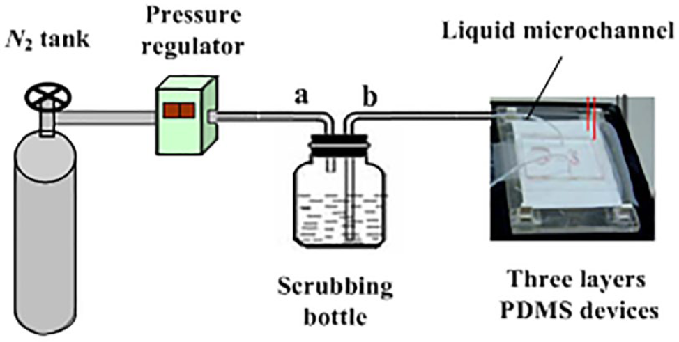
Diagram of fluid-driving setup.
Design of the Three-Layer Microfluidic Chip
The liquid sample system, designed for testing the manufacturing and packaging effect, including the basic active functions of microchips, consists of the microfluidic chip with integrated two microvalves, a micromixer, and an S-shaped peristaltic micropump. The pneumatic microfluidic chip has two layers of microchannel networks. The top liquid layer has the fluidic microchannels, which consist of two sample reservoirs, a Y-shaped junction for converging, a square chamber for mixing, and a gathering reservoir. The two samples come in through the sample reservoirs separately, pass through a flow-focusing unit, and after intensive mixing and sufficient reaction, flow to the gathering reservoir under the power of the S-shaped peristaltic micropump ( Fig. 2c ). The bottom control layer has the air microchannels that control the integrated microvalves, the micromixer, and the peristaltic micropump. Figure 2a,b shows a schematic of the design size of the control layer and liquid layer separately.
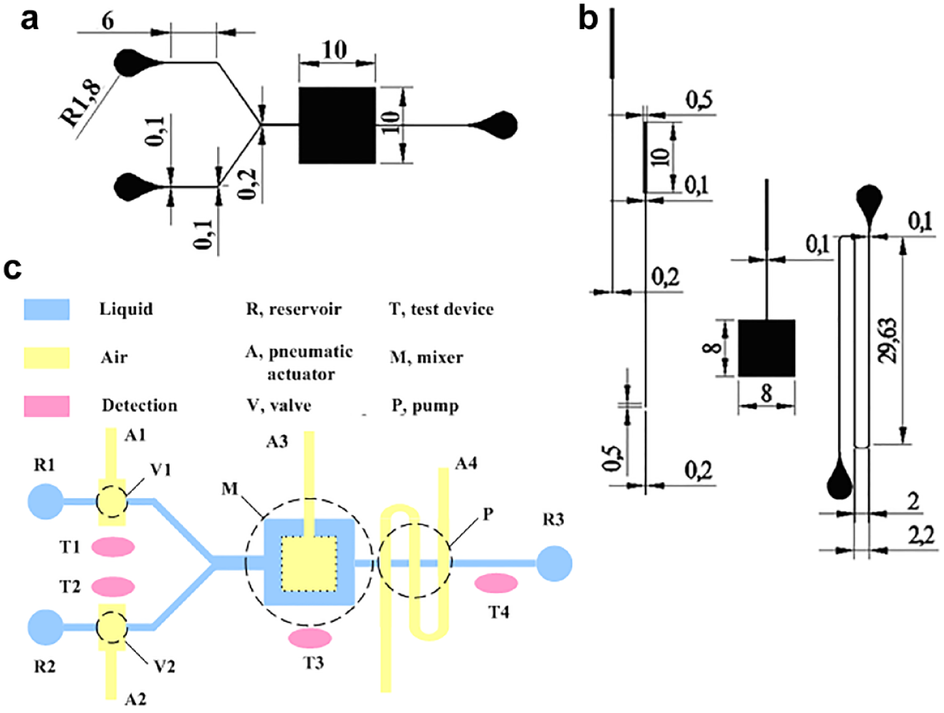
Schematic of the design size of the pneumatic microfluidic chip. (
Fabrication of a Three-Layer Microfluidic Chip
The structure is designed by CAD software and printed onto the photo film using a high-resolution inkjet printer as a photomask. The mold fabrication process employs a permanent dry film with 50 μm thickness instead of SU-8 liquid photoresist; this fabrication method is cheaper and simpler and takes less time than other popular ones. Figure 3a illustrates the specific fabrication process employed for the mold with rectangular cross section microchannels using a dry-film negative photoresist on a stainless steel wafer. The fabrication starts with the mold production using a dry-film negative photoresist, which is dry film made of a negative thick photoresist, which is pressed onto a stainless steel wafer to form a 50 μm thick layer using a sealing machine at room temperature. Then, the pressed wafer is cured for 10 min at 80 °C in the oven. Then it is taken out and allowed to cool down. When the surface temperature of the pressed wafer drops to room temperature, another layer with the same thickness (50 μm) of dry-film negative photoresist is pressed on the wafer. Next, the steel wafer is pressed five times with a 100 μm thick dry-film negative photoresist using the sealing machine at 100 °C, in order to firmly fix the dry-film negative photoresist on the stainless steel wafer. The wafer is covered with a photomask and exposed 10 cm away from a UV lamp for 110 s. The exposure time under the UV light depends on the UV intensity and dry-film thickness of the mold. In this work, the power of the UV lamp is 25 W. Underexposure will lead to fuzzy development and make the unexposed part difficult to rinse in the next step, and overexposure will harden the exposed part and cause poor adhesion. Exposure for 90 s is suitable for one layer of 50 μm thick dry film using the same UV lamp. For sufficient image development, soak the wafer in Na2CO3 solution (1:70) for 5 min. Then rinse the wafer several times using anhydrous alcohol and deionized (DI) water, respectively, followed by a blow-dry process using compressed N2. Next, a postexposure bake at 80 °C is performed for 5 min. If the bake time is less than 5 min or the baking temperature is higher than 150 °C, the dry-film negative photoresist on the mold will become brittle and easily detach from the wafer. The process of dry-film negative photoresist mold fabrication can be completed within 1 h, and the manufacturing environment does not require a clean room. Furthermore, the mold fabrication only needs an inexpensive dry-film negative photoresist and related common office facilities.
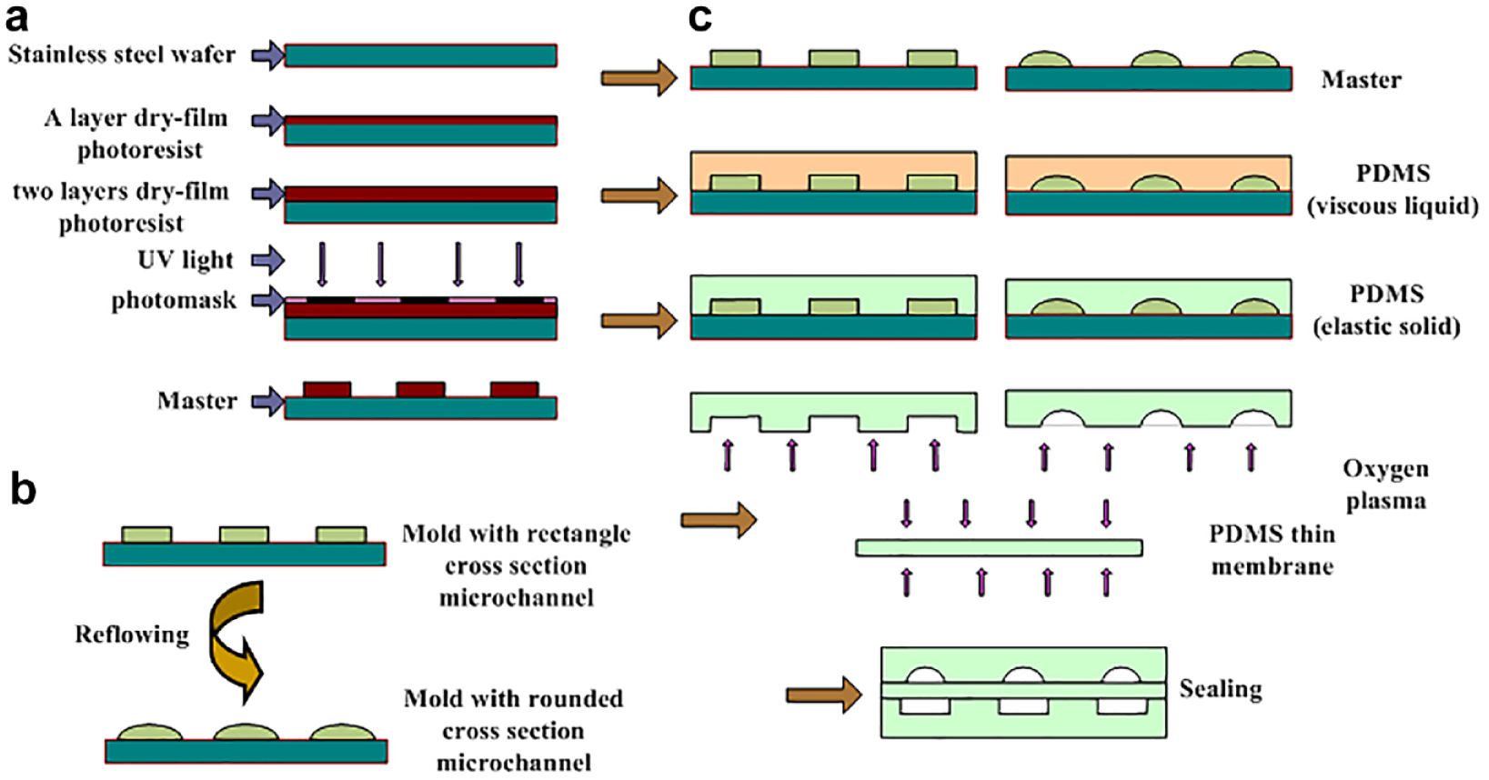
Protocol for the specific fabrication process. (
The experimental equipment required for fabricating a mold with rectangular cross section microchannels using a dry-film negative photoresist is ordinary office facilities, rather than professional experimental equipment. Therefore, there are some difficulties to overcome: (1) The most suitable distance and time between the UV lamp and dry film during exposure may require many experiments to find. (2) When using the sealing machine for multilayer bonding, the sealing temperature is a key factor and decides the degree of adhesion between dry-film layers. (3) The dry-film photoresist must be protected from light. When cutting a dry-film photoresist, avoid light and minimize the amount of time it takes. Otherwise, the dry-film photoresist will be partially exposed before use. The preexposure steps should be completed in the shortest possible time.
In order to fabricate high-aspect-ratio fluidic microchannels, we spin-coat a thick positive photoresist (AZ 50 XT) on a 4 in. silicon wafer and pattern it by standard photolithography. Once developed, the photoresist is heated above its glass transition temperature (120 °C), thus allowing reflow of the positive photoresist in order to obtain microchannels with a rounded cross section, as shown in Figure 3b . The reflow temperature and time combined with the width of the microstructures on the mold affect the arc level of the mold.
There are some difficulties to overcome for fabricating a mold with rounded cross section microchannels using an AZ 50 XT-positive photoresist: (1) The spin-coat equipment and the exposure platform must be maintained absolutely level; otherwise, the microchannel’s depth on the same mold will not be consistent. (2) The reflow temperature and time of AZ 50 XT for different microchannel depths are obtained by conducting several repeat experiments. (3) Keeping the surface clean under common laboratory conditions is also a challenge because of a certain viscosity on the cured positive photoresist surface.
Briefly, the middle layer of the PDMS thin membrane is spin-coated on the planar side of a silicon wafer, spin-coating an about 40 μm thick PDMS from a prepolymer solution (base/curing agent 15:1) by the spin coater at 1500 rpm. Then, the filled mold is cured for 3 h at 65 °C in the oven. Less curing of the PDMS prepolymer and a longer and lower cured temperature can increase the thin membrane toughness. The control layer and liquid layer are made by replica casting of the prepolymer solution (base/curing agent 5:1) on their molds separately, which are then cured for 30 min at 80 °C in the oven. More curing of the PDMS prepolymer and a shorter and higher cured temperature can improve the plasticity of the thick PDMS slab and help the thick PDMS slab better support the whole microfluidic chip. The different ratios of the two layers of the cured PDMS also have a significant influence on the bonding strength. Cut and punch them. Then the PDMS slabs with microstructure networks and the PDMS thin membrane are treated by a 50 W plasma for 2 min. Align the three layers and seal them into a whole microfluidic chip within 2 min, gently pressing with tweezers. The encapsulated process is shown in Figure 3c .
Results and Discussion
Control Layer Mold Manufacturing Results
We first carried out experiments on test microstructure sizes on the control layer molds, in order to check and correct our fabrication process in terms of the differences between the designs and manufactured objects. We tested different sizes of several kinds of microstructures to find the manufacturing error. Examples of microstructures on the mold obtained using our processes are presented in Figure 4 . These results were obtained on stainless steel wafers and measured by a stereomicroscope (MA2003A; Shenzhen Mashide Equipment Company, Shenzhen, China). The design sizes of the microstructures were 300, 500 × 500, and 300 × 500 μm, respectively. The measured dimensions were 298, 490 × 478, and 297 × 489 μm, respectively. From the results we derived the following main conclusions: (1) All measurements are slightly smaller than their design values. (2) The maximum error between the design and real values is 4%. Sizes smaller than the design may have resulted from the exposure light that is not vertical. The maximum error is acceptable for microfluidic fields. In the field of microfluidics, the acceptable maximum error range is 5%. We also measured the thickness of the microstructures on the mold; the mean thickness was 49.8 μm (the nominal thickness of a single-layer dry film is 50 μm). The slight error may have been caused by manufacturer calibration fault, or possibly because of adhesive matter volatilization between the dry film and its protected layers.
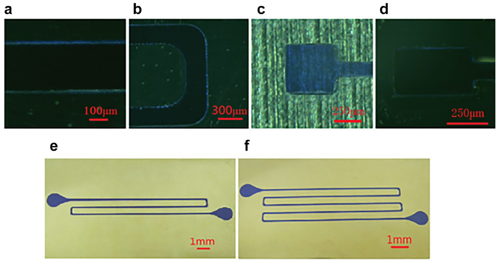
Microscope images of rectangular cross section molds. (
Liquid Layer Mold Manufacturing Results
The stereomicroscope is used to observe and capture images of the microstructures on the molds. The reflow temperature and time combined with the width of the microchannels on the molds affects the arc level of the molds. In this regard, the mold with the width of 100 μm microchannels needs a reflow temperature of 140 °C for 5 min, the mold with the width of 300 μm microchannels needs the same reflow temperature for 3.5 min, and the mold with the width of 500 μm microchannels needs the same reflow temperature for 3 min. Figure 5a–d shows the microscope images of micropatterned features of lines and crossbars made by the positive photoresist. In the images the arc effect of the microstructures is very obvious.
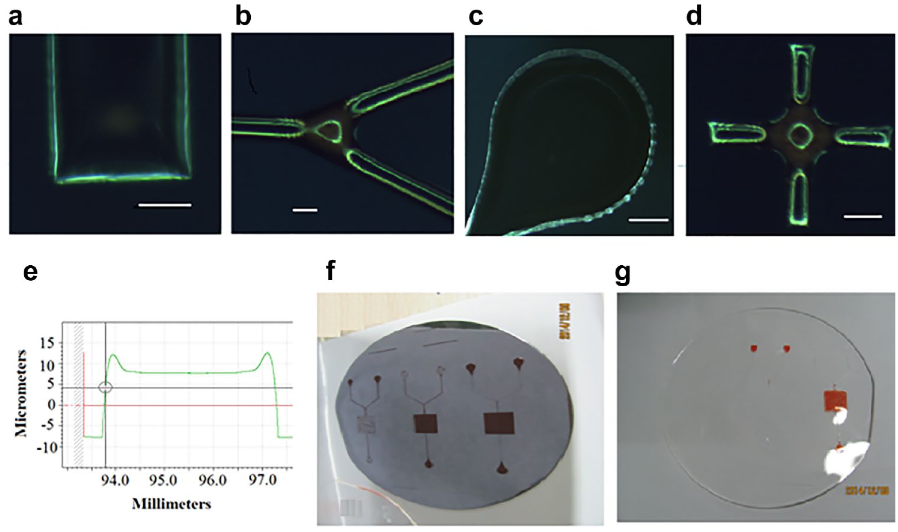
Microscope images of rounded cross section molds. (
In the process of conducting positive photoresist reflow experiments, we found that a suitable temperature is the most critical parameter in the production process. If the reflow temperature is higher than 150°C, the arc level and surface profile are difficult to control; a cat ear shape appears on top of the microchannel on the mold ( Fig. 5e ). It is important to note that excessive temperature causes aging of the positive photoresist and detachment from its substrate when copying the microchannels by PDMS materials. In addition, too high of a temperature leads the solid positive photoresist to disintegrate into powder. For example, when the reflow temperature is up to 180 °C for 3 min, the cured positive photoresist on the mold becomes deep red in color (normal is brown and transparent) and easily detaches from its substrate after one or two uses, as shown in Figure 5f,g . The reason for this phenomenon is that too high of a reflow temperature can lead to cured positive photoresist flow again, rather than its glass transition, resulting in weak adhesion to the stainless steel wafer. In addition, the color change of the cured positive photoresist is caused by too much heat radiation.
For further quantitative analysis of the arc effect, the microchannels’ surface microtopography of the molds is observed by a surface profiler (Form Talysurf PGI 1240; Taylor Hobson Co., Ltd., Leicester, England). Figure 6 shows surface profiles, cross section pictures, and platforms of the three different dimension microchannels on the molds with a rounded cross section. Three different widths of microchannels on a liquid layer mold are measured by the surface profiler and stereomicroscope. The designed widths are 100, 180, and 250 μm, respectively. After reflow, the measured widths are 128, 202, and 276 μm, respectively. From Figure 6 , the surface profiles of the microchannels on the mold are similarly parabolas, the trends are smooth, and there are no obvious bumps or pits on the mold’s surface.
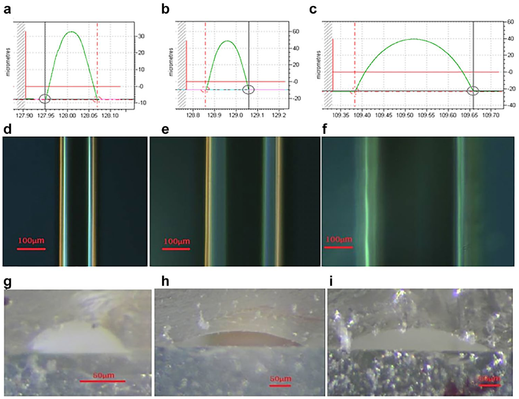
Surface profiles (
Bonding Results
The method for sealing microfluidic chips made from PDMS material is much easier and simpler than the methods used for other commonly rigid materials, such as glass, Si, and polymethyl methacrylate (PMMA). It includes reversible and irreversible seals for PDMS microfluidic chips. Because the this method is sufficiently strong for the high-pressure pneumatic microfluidic chip and the designed chip in this paper does not need to be cleaned because of the dry and clean N2 being used, the mixed sealing method of oxygen plasma treatment bonding and PDMS varying ratio bonding reinforces the sealing strength.
A coarse detection method for the sealing strength of the PDMS device is given here. An inlet of the proposed chip is connected to an air supply. Another inlet and an outlet tube are closed by cured PDMS blocks, and the device is kept slightly submerged in the DI water. The decompression device on the air tank is regulated from 0 to 280 kPa. There is no continuous or large bubble overflow that can be detected by the naked eye. After 20 min, there is no significant change of the digital pressure gauge number. This indicates that the designed chip can sustain the airflow of an applied pressure of 280 kPa without leaking, which makes it fully able to satisfy the needs of pneumatic microfluidic chips, because the air pressure of pneumatic microfluidic chips is normally lower than 150 kPa.
Experimental Performance of Pinching Off and Mixing
In order to pinch off fluids in microfluidic systems with a liquid layer and a control layer, a pneumatic microvalve typically consists of a pneumatic actuator in the control layer and a microfluidic microchannel in the liquid layer, and the two microchannels are placed vertically after encapsulating the integrated microfluidic devices, as schematically shown in Figure 7a . The two layers are separated by the elastic PDMS thin membrane. The control layer and its top membrane constitute a pneumatic actuator, as shown in Figure 7b . The deflection of the thin PDMS membranes and the actuation of pneumatic actuators are controlled by the pressure of compressed air, which is supplied to the actuators through the pneumatic control microchannels linked to the pneumatic actuators.
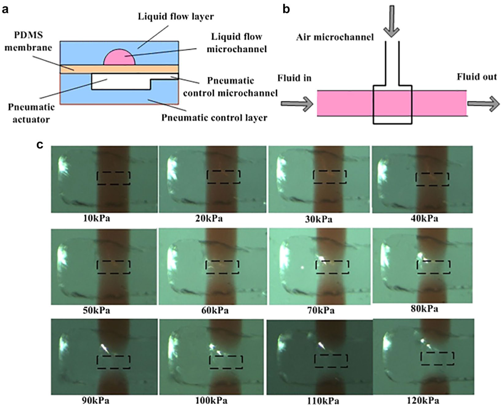
Schematic and pictures of the pneumatic microvalve. (
Before the experiments, the microdevice is washed with DI water for 10 min, because the N2 in the microchannels could result in clogging and must be pushed out. We observe the pinching results under different actuated pressures ( Fig. 7c ). Note that the actuated region of the pneumatic actuator is 297 × 489 μm, and the width of the liquid microchannel is 276 μm. A dark or light red color indicates the depth of the liquid and reflects the valve openings of the microvalve. We expended considerable effort in developing a protocol to test the microvalve under air microchannel inlet pressures in the range of 0 to 120 kPa in 10 kPa increments. The valve opening of the microvalve is determined by the actuated pressure. From the test screenshot we can clearly see that when the actuated pressure increases, the degree of red color in the dotted line area becomes lighter, and the valve opening of the microvalve becomes smaller. The microvalve starts in the closed state when the actuated pressure is equal to 70 kPa and the depth of the liquid microchannel is 62.6 μm. With the increase of actuated pressure, the width of the closed microvalve (along the direction of liquid flow) is larger. The PDMS can be approximately considered incompressible, highly elastic nonlinear material, and the deformation of the PDMS membrane is far beyond its thickness, which fully conforms to the large-deformation theory. When the actuated pressure is smaller than the closed pressure of the microvalve, the deformation of the PDMS membrane tends to be semiellipsoidal. With the increase of actuated pressure, the deformation of the PDMS membrane in the width direction extends along the center line to both sides in a parabolic trajectory, and the deformation along the length direction is ignored, and the PDMS membrane deformation basically conforms to the plane strain theory.
Figure 8a shows a schematic illustration of the micromixer consisting of two PDMS layers. The top PDMS liquid layer comprises a mixing chamber. The bottom PDMS control layer contains a pneumatic actuator with a connecting air microchannel. When compressed air is supplied to the pneumatic actuator, the thin (40 μm) PDMS membrane can be deflected upward, and the deflectable diaphragm recovers after the air pressure is removed, because of its elasticity and the weight of the liquids in the mixing chamber. This can generate a vortex-type flow inside the mixing chamber. The thin PDMS membrane can move up and down continuously by injection of the compressed air into the air chamber through the connecting air microchannel. The air chamber pressure is controlled by an off-chip three-way electromagnetic valve. The driving frequency of the electromagnetic valve can be regulated utilizing a microcontroller by providing the digital signal to the electromagnetic valve. We have taken photographs of every dye color and DI water fully filled with the mixing chamber by the stereomicroscope, separately, as illustrated in Figure 8b .
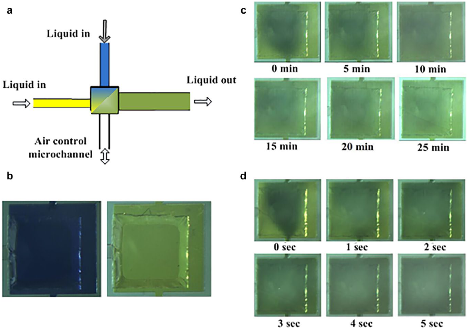
Pictures of the microchannels filled with liquids and two series of a microscope in two micromixing chambers. (
Before experiments, the microdevice is washed with DI water for 10 min to push out air bubbles in the mixing chamber. The mixing results are recorded by taking photos in the retry time interval using the stereomicroscope. About 0.04 μL of DI water of with yellow dye and 0.02 μL of DI with blue dye are pipetted into the mixing chamber by a suit of fluid driving the setup, which was described. Figure 8c shows a series of photographs for free convection in the micromixer at different times. The change of color intensity for the color dyes shows that almost complete mixing of the samples has been achieved. According to the color of the microscope images, we can see that the two liquids with different colors have not yet fully mixed after 25 min, under the condition of the free convective mixing process. Figure 8d shows a series of photographs for the vibrating mixing process at different times. The liquid samples can be rapidly mixed by the micromixer. The applied pressure and driving frequency are 20 kPa and 1 Hz, respectively, for this case. These pictures prove that the two liquid samples with different colors are almost completely mixed after four times shock. The mixing efficiency is found to be dependent on the mixing time and driving frequency, while the applied pressure is kept constant. As expected, the mixing efficiency is also dependent on the applied pressure since it determines the deformation of the membranes. Experiments show that it only three times shock is needed to fully mix the same liquids when the air pressure in the pneumatic actuator is 30 kPa. However, when the air pressure exceeds 30 kPa, there is no obvious change in the mixing number needed (three times shock). This is caused by the influence of the PDMS membrane; the effect of excess displacement under a higher actuated pressure on mixing efficiency is negligible. It should be noted that the mixed test in microscale is completed under the conditions of low vibration frequency (less than or equal to 1 Hz). This is because the air control microchannel of the micromixer is relatively narrow, and the flow resistance is relatively large, resulting in a relatively long air filling and exhaust time.
Conclusions
The goal of fabricating a three-layer microfluidic chip for the pinching off and mixing of liquid samples has been reached; the control layer is fabricated by a dry-film negative photoresist mold, and the liquid layer is fabricated by a positive photoresist reflow technology, followed by the sealing of the two layers and the thin PDMS membrane together to construct microchannel networks. Complete bonding is achieved at room temperature without other special conditions. Liquid sample pinching and mixing experiments were conducted to evaluate the properties of a three-layer PDMS pneumatic microfluidic chip. The microfluidic chip in this paper can sustain N2 flow at an applied pressure of 280 kPa without bursting open. This fully satisfies the air pressure needs of a pneumatic microfluidic chip.
The pinching-off microchannel networks are constructed by one + unit. The cross section area can realize the pinching off of the flow of fluids above it and act as a pneumatic microvalve; its valve openings are precisely controlled by controlling the pneumatic pressures, to accurately control liquid sample flow rates. The unchanged dye color flow rates demonstrate the fluid cutoff conditions. The mixing microchannel networks are designed based on the hybrid theory of vibration. The change in color intensity for the dye colors shows that an almost complete mixing of samples has been achieved. The successful testing in this paper of active functions in integrated microfluidic chips, such as pneumatic microvalves and pneumatic micromixers, shows that the purpose of designing and fabricating has been easily realized: to save energy and cost and be more efficient.
Footnotes
Declaration of Conflicting Interests
The authors declared no potential conflicts of interest with respect to the research, authorship, and/or publication of this article.
Funding
The authors disclosed receipt of the following financial support for the research, authorship, and/or publication of this article: This work is supported by National Natural Science Foundation of China (no. 51175101), Key Scientific and Technological Project of Henan Province (no. 192102310046), and Doctoral Research Fund of Zhengzhou Institute of Light Industry (no. 2016BSJJ015).