
Abstract
Subject material presented describes substrate materials and their processing as key elements in microsystems technology manufacturing (MST) for Biochips (DNA arrays), Electronic MEMS (Micro-Electro-Mechanical) Devices and electro-optics. Material choices are primarily glass, quartz and silicon, each of which may require mechanical features and exact surface finishes to enable design function and manufacturing. This paper will address some basic approaches to determining what substrates require for specific designs and manufacturing processes.
INTRODUCTION
As engineers and scientists design prototype devices, they are challenged with the task of deciding what material best meets their requirements. Considerations of the type of mechanical, physical, and chemical machining will provide the critical features, determine the optimum substrate material choice.
This list of materials is generally used for applications requiring the following physical attributes:
This paper will deal with the requirement of hard surface substrates with and without features, with a focus on gass and fused silica.
Once substrate material is decided on, the following decisions can be determined. The table below shows materials, fabrication and assembly processes for microsystems.
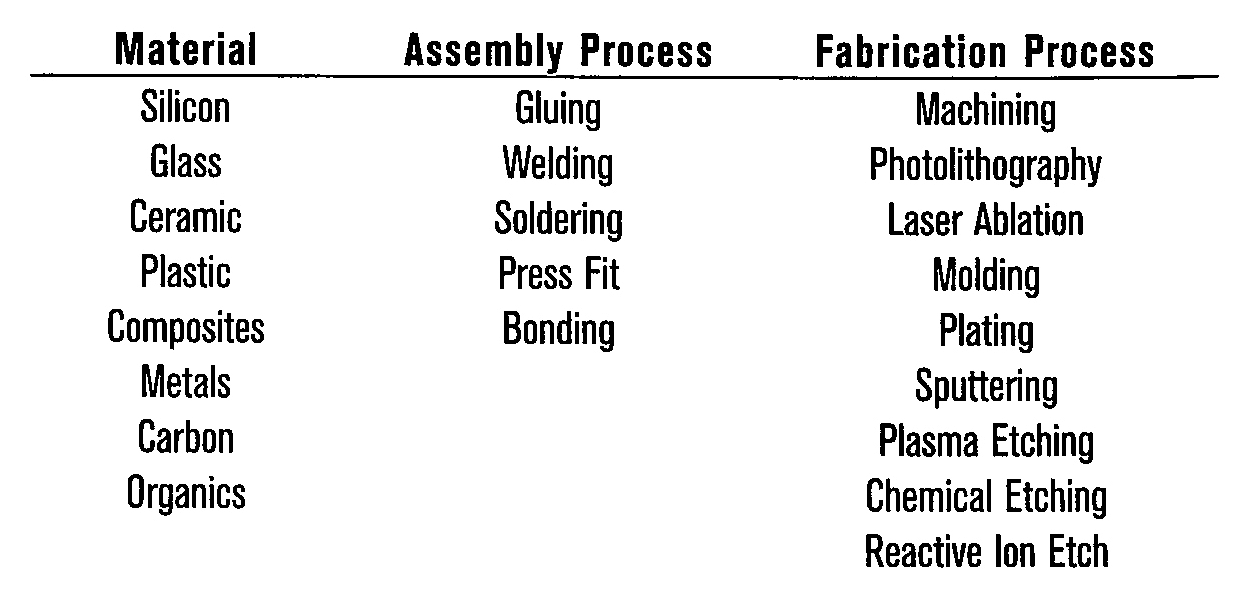
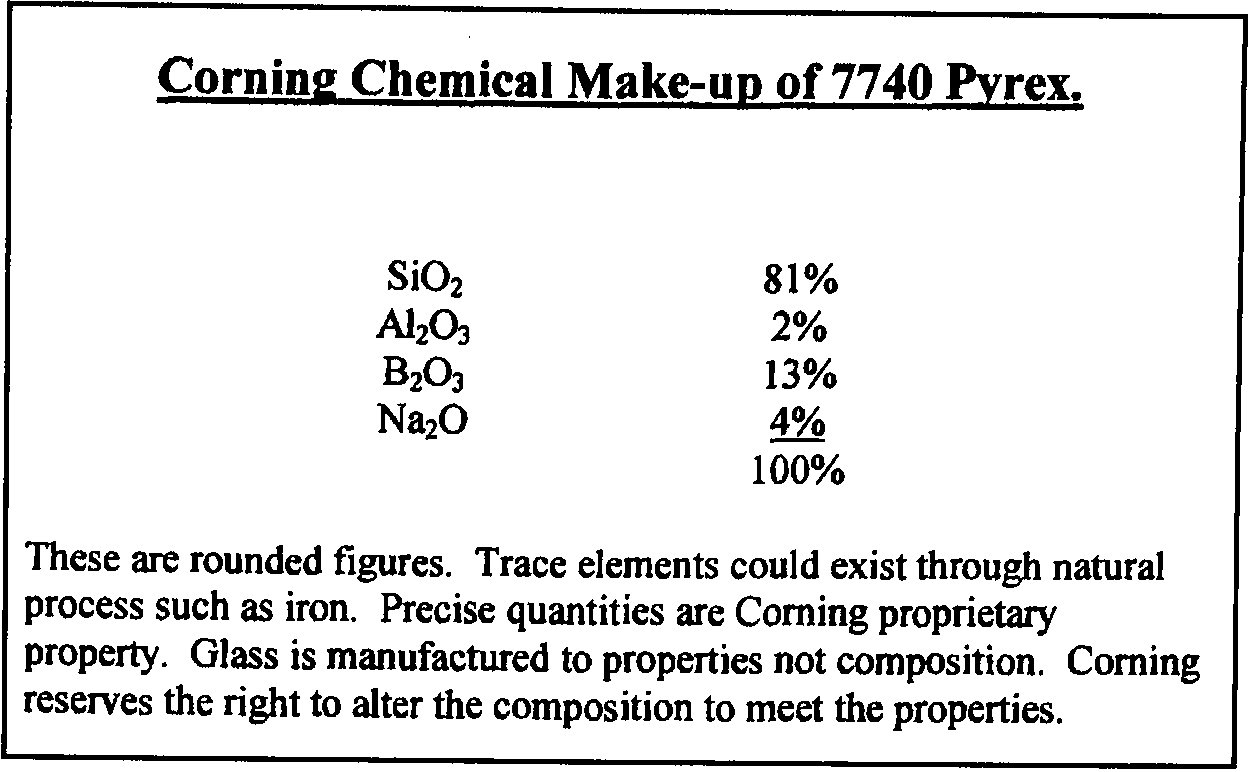
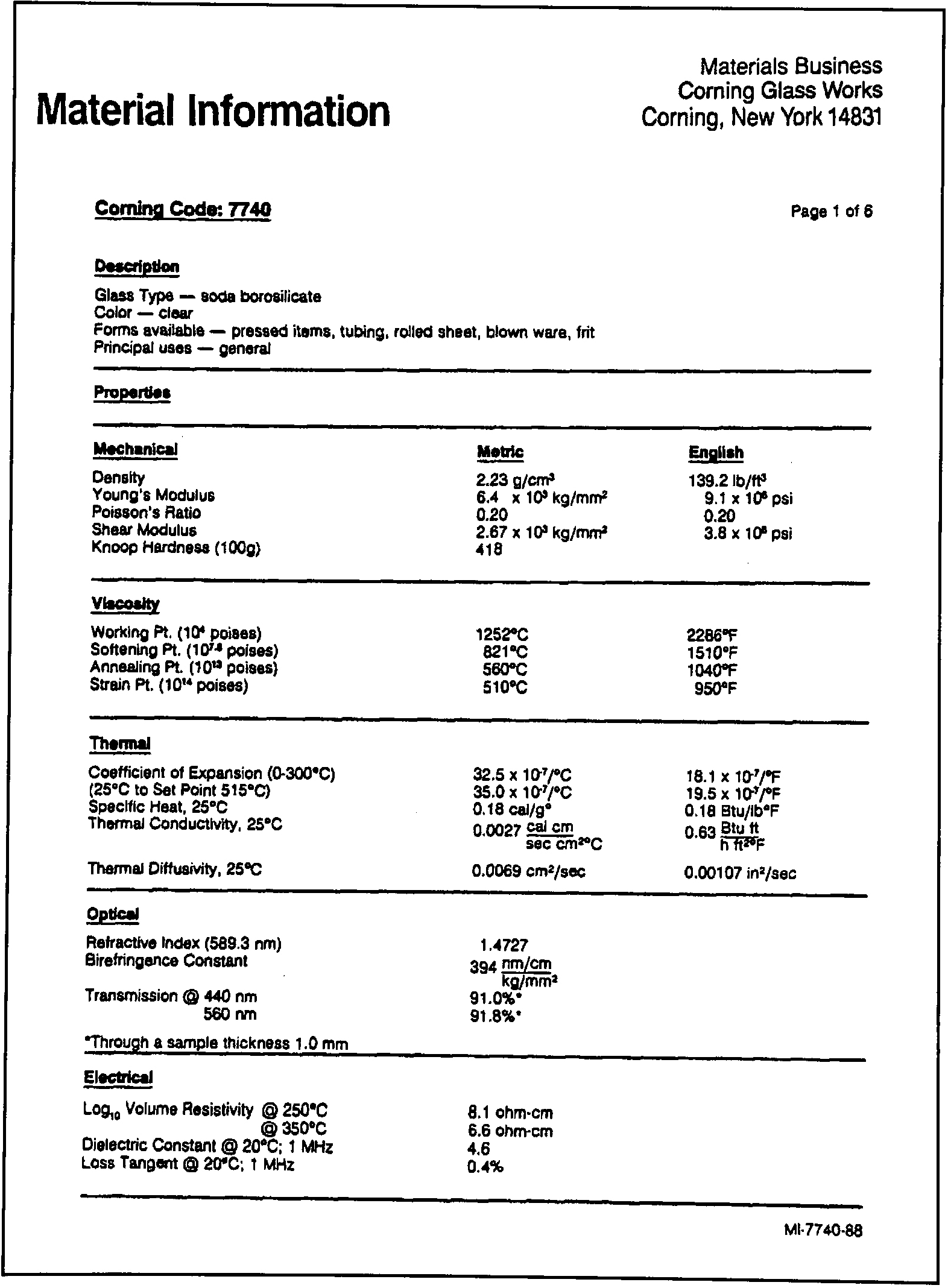
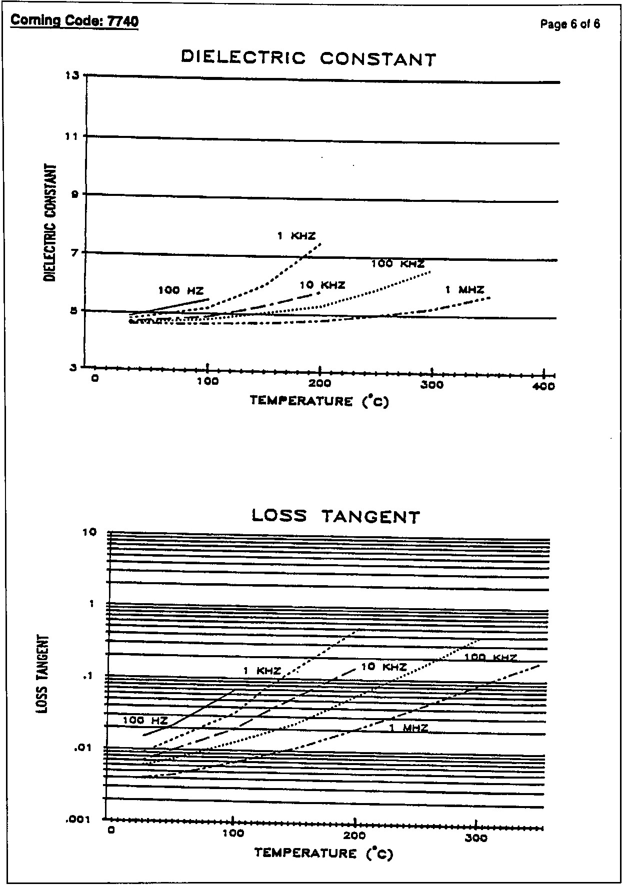
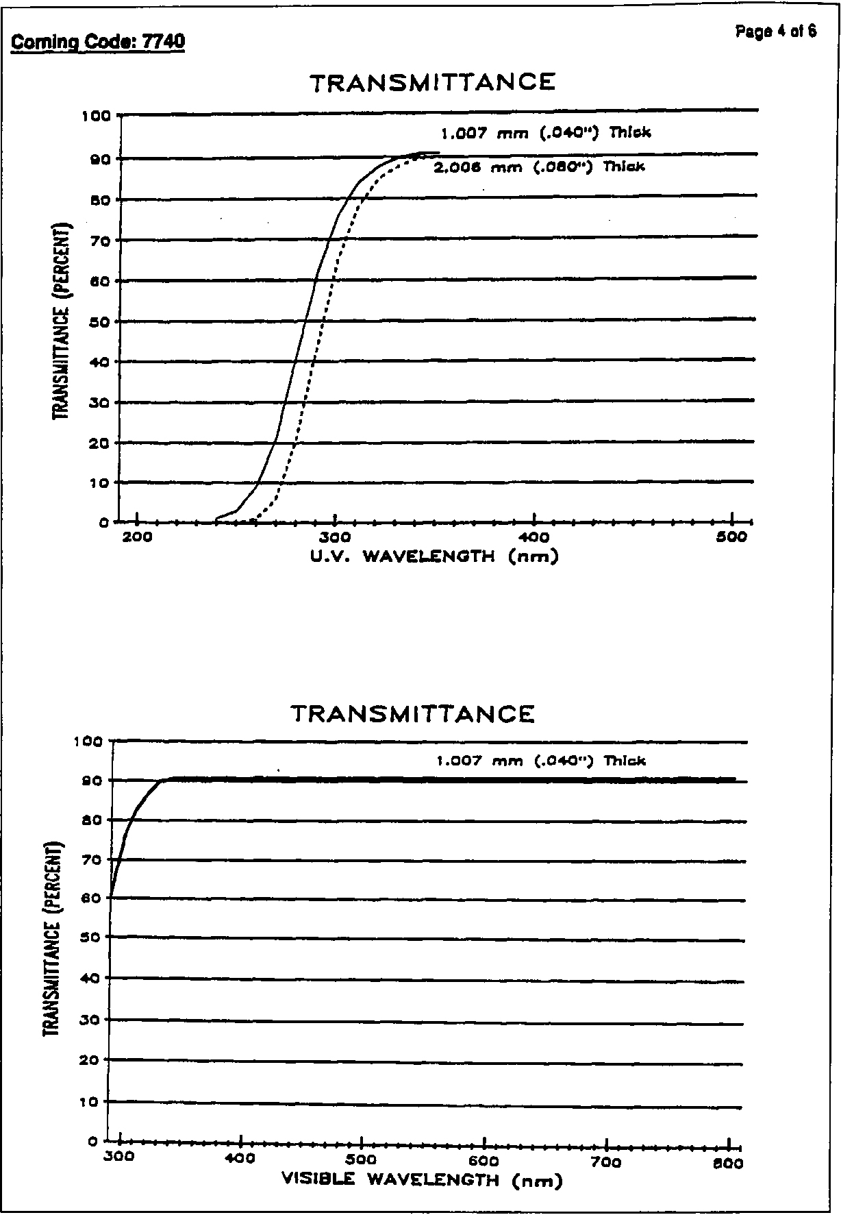
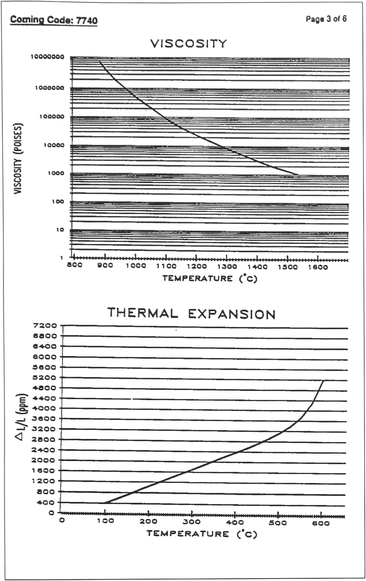
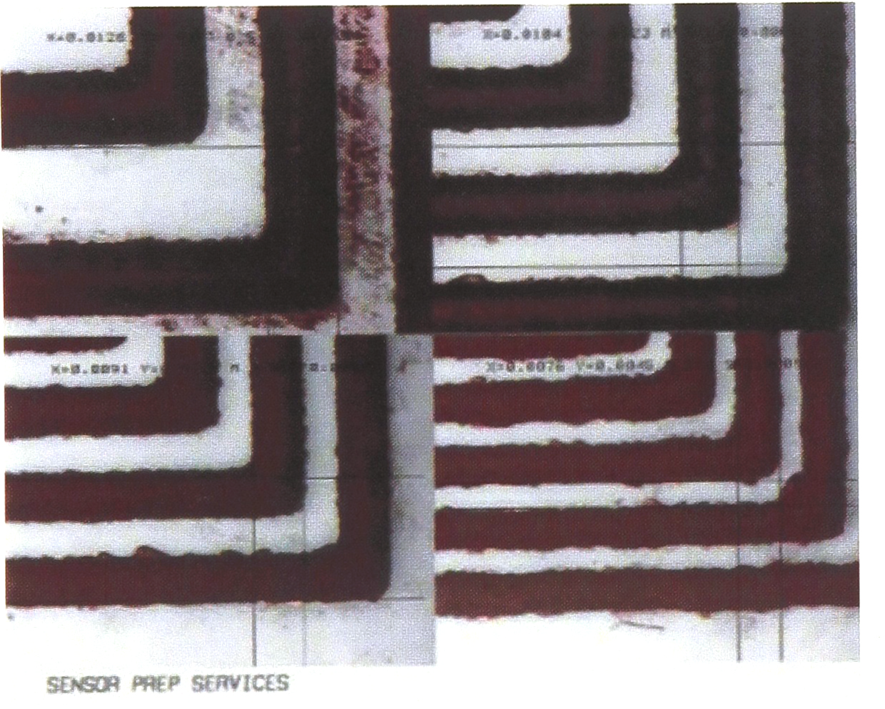
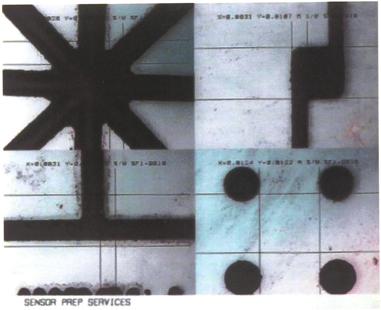
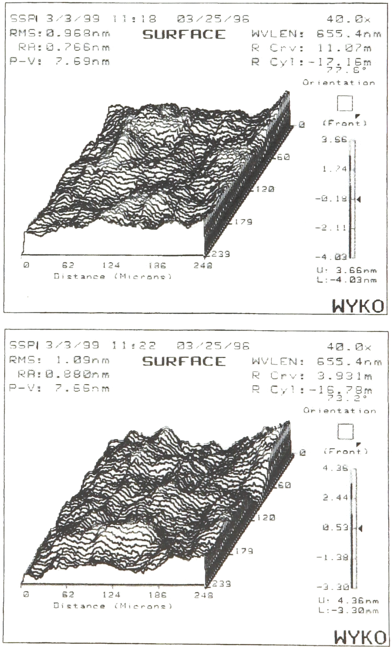
A typical start for a device consideration begins with working on a single piece of glass or silicon. If the glass is to be anodically bonded to silicon or fused with another piece of glass the following must be considered. The glass must have a relative thermal expansion coefficient that closely matches up to that of the silicon. (Figures 2-5)
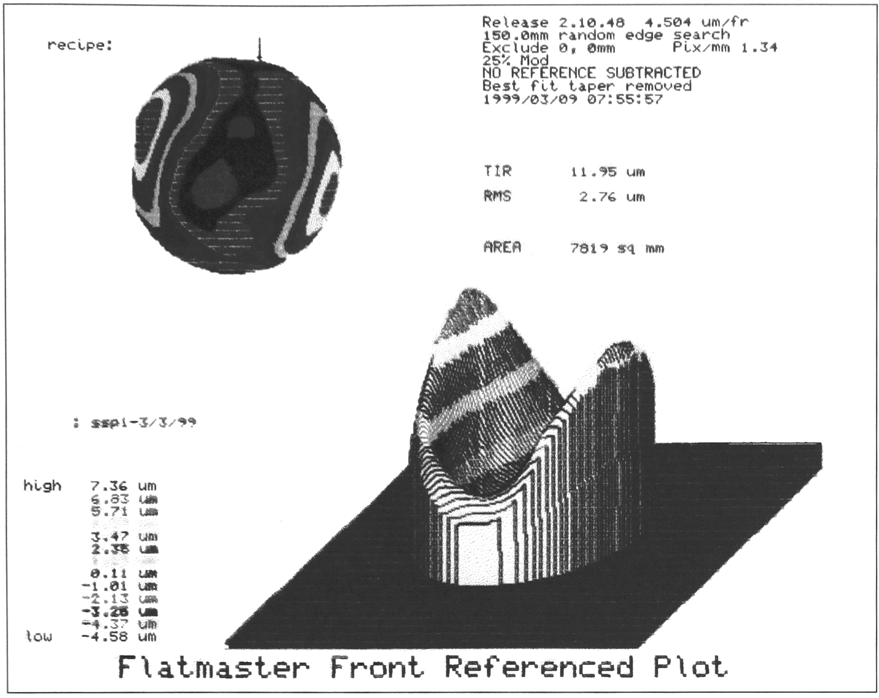
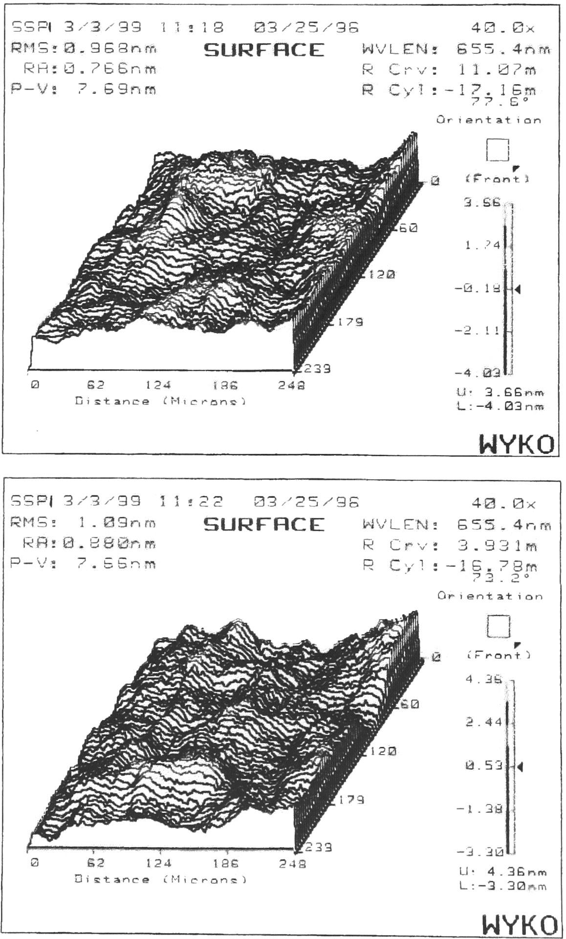
Silicon to glass wafer bonding requires exact surface smoothness to prevent voids in the bonding interface. If the glass or silicon has high surface roughness or exceeds a critical value, the wafer will not bond properly. A variety of bonding methods such as: bonding at room temperature to bonding in a high temperature (400°C) in a vacuum and pressure will determine some basic parameters'. Typical substrate surface roughness values stated as Ra range from 15–20 angstroms (average) to 8–10 angstroms bondable to 4–8 angstroms bondable and etch able. These surfaces can be specified and determined by utilizing optical interferometers and profilometer surface detection devices. Atomic Force Measurement (AFM) can also be utilized if one has access. Flatness of the substrate will also effect the bondability of the material. Flatness is often expressed as Rms and refers to the overall peak to valley (highest to lowest) measurements that will reduce bondability. Glass substrates can be purchased directly from companies that will specify the surface roughness and flatness parameters to meet a range of requirements
Charged particles adhere to glass.
Ions from glass and cleaning solutions will migrate to new surfaces.
Particles will contaminate surfaces.
Material handling issues will cause surface scratches.
Ion exchange or transference to base material.
It is recommended that end users clean incoming materials. It is best to work with a supplier to define cleaning and packaging requirements to prevent permanent damage to wafer surfaces.
CONCLUSION
The relationship between substrate materials, machined features, surface finishes and device design is important to function and cost. Most designers work with materials they have experience with, however they may not be familiar with current machined feature capabilities that would enable them the opportunity to produce a more advanced device at a reasonable cost.
As microsystems technology grows, there is more information available through a number of organizations relating to materials, processes and suppliers providing services to technically assist those developing their unique devices.