
Abstract
Multi-step chemical vapor deposition (CVD) is a synthesis method which is capable of producing a uniform, large area, and high-quality thin films. In this work, we report the effect of post-annealing on the structural and optical properties of few-layers (FL) MoS2 thin films synthesized by multi-step CVD. Based on atomic force microscopic image, the thickness of the MoS2 thin film is ∼3 nm, which is equivalent to five layers. After annealing at 900°C for 17 min, intensity of the A1g and
Introduction
Two-dimensional (2D) transition metal dichalcogenides (TMDs) have received significant interest due to their unique and diverse properties which are useful for fundamental studies and various electronics and electrochemistry applications. 1 –7 Semiconducting 2D TMDs such as MoS2, MoSe2, WS2, and WSe2 are favorable for realizing ultrasmall transistors due to their finite bandgap which is not found in graphene. 8 –10 Bulk MoS2 is an indirect bandgap material (∼1.2 eV) but the bandgap energy increases to ∼1.8 eV and becomes direct when the thickness reduces to monolayer. 11 Although monolayer MoS2 has been the main subject of interest, few-layers (FL) MoS2 also exhibits relatively good performance. For field-effect transistor (FET), five-layer MoS2 devices with electron mobility of 70 cm2V−1s−1 have been reported and high drive current of 24 μAμm−1 has been achieved with a top-gate FET configuration. 12,13 Photodetector based on FL MoS2 on p-type Si also has been shown to have photoresponsivity of 0.141 AW−1 at −2 V which is higher than previously reported photoresponsitivity of other TMDs (2.12 × 10⁻⁵-0.133 AW−1). 14 –17 Besides, MoS2 film also can be transferred onto a flexible substrate such as polyethylene terephthalate to make flexible devices. Even though the response time of MoS2 flexible photodetector is still relatively slow (seconds), the photoresponse is similar in both flat and bending states. 18
One of the key advantages of FL MoS2 is that the synthesis is less stringent and require less precision compared to its monolayer counterpart. 19 In this work, multi-step chemical vapor deposition (CVD) has been chosen due to its scalability and ability to produce a uniform and continuous MoS2 thin films. This method consists of two main steps: deposition of Mo-based film on substrate and then followed by sulfurization process to produce MoS2 thin film. The MoO3 layer is typically coated or deposited by spin coating, atomic layer deposition (ALD), or thermal evaporation. 20 –22 While spin coating is the fastest and simplest method, the thin film uniformity is the lowest. ALD allows precise control of layer thickness, but the process is complex and costly. Thermal evaporation of MoO3 is a simple process and can provide a uniform thin film throughout the substrate.
For multi-step CVD, a post-annealing step is typically required to improve the crystal quality of the grown film. Heo et al. showed that post-annealing temperature can influence the carrier transport in MoS2 thin film FET. 23 At a post-annealing temperature of 600°C, the transistor is ambipolar while at 1000°C, n-type transistor is obtained. Besides, electron mobility also improved from 3.4 × 10⁻⁵V−1s−1 to 2.0 × 10⁻¹ cm2V−1s−1 after annealing at 1000°C and it was attributed to improved crystallinity of the film and reduction of excess sulfur atoms. Heo et al. gave a great emphasis on electrical characterizations while the effect of high-temperature annealing on the structural and optical properties of FL MoS2 thin film was not studied in depth. In this work, we report a detailed study on the synthesis and characterization of FL MoS2 thin films prepared by multi-step CVD. The effect of high-temperature annealing on structural and optical properties of MoS2 thin films also will be discussed.
Experimental details
The MoS2 thin films were synthesized by multi-step CVD and the procedure is illustrated in Figure 1(a) to (d). First, 3 nm of MoO3 film was deposited on sapphire substrate in vacuum at a pressure of 10−3 Pa by thermal evaporation (Figure 1(a)). The MoO3 deposition rate was stabilized at 1 Å/10 s before deposition to ensure uniformity of the thin film. Next, the MoO3 film was annealed in oxygen ambient at 325°C for 2 h (Figure 1(b)). The sulfurization process consists of two stages. In the first stage, after S powder (800 mg) and the MoO3 sample were loaded into zones 1 and 2, respectively, nitrogen gas was fed into the quartz tube at a rate of 2 Lmin−1 until the pressure in the system reaches ∼10 kPa. Then, zone 1 which contain S powder were heated to 275°C and zone 2 to 180°C and maintained for 10 min. This is to ensure that the tube is filled with S vapor before sulfurization. For the second stage, zone 2 were heated further to 550°C and pressure of the system was increased to ∼125 kPa. The sulfurization temperature (550°C) and pressure have been optimized from our earlier studies. 7,20,23 The temperature and pressure were maintained for 1 h to sulfurize MoO3 to MoS2. Temperature at zone 1 was maintained at 275°C throughout the whole process. Subsequently, the MoS2 film was annealed at 900°C for 17 min in nitrogen ambient (Figure 1(d)). To reduce desorption of S during annealing, a sapphire covering plate was placed on the sample. 23

Procedure for multi-step CVD of MoS2: (a) thermal evaporation of MoO3 film (3 nm), (b) first annealing in O2 ambient, (c) sulfurization and (d) post-high-temperature annealing in N2 ambient, (e) optical image of the annealed MoS2 top-gate FET, and (f) schematic of the device cross section.
Then, the samples were analyzed by using a confocal micro-Raman imaging spectroscopy (DXR2Xi, Thermo Scientific, Massachusetts, United States) with 532-nm laser source and laser spot size of ∼1 μm. A relatively low laser power was used to ensure no damage to the thin films. X-ray diffraction (XRD) was carried out using a Bruker D8 Advance operating at 40 kV and 40 mA with copper K α radiation (λ = 1.5406 Å). Optical characterization of the MoS2 thin films was performed using ultraviolet–visible spectroscopy (Lambda 950, PerkinElmer, Massachusettes, United States). Thickness and surface roughness were measured using atomic force microscopy (AFM) in tapping mode by Hitachi AFM5100N, Japan.
Top-gated MoS2 FETs were fabricated using lithography-free technique. 20,23 A patterned MoS2 thin film was prepared by covering the substrate with a shadow mask during deposition of MoO3 and then annealed. 20 Next, source and drain electrodes (30 nm of Au) were deposited by thermal evaporation using a shadow mask. The length and width of the channel are 100 µm and 400 μm, respectively, as shown in Figure 1(e). Then, 25-nm-thick Al2O3 gate dielectric was deposited using ALD. Lastly, top-gate electrode (30 nm of Au) was deposited using thermal evaporation through a shadow mask. Figure 1(f) shows the schematic cross section of the MoS2 thin film FET. One of the main limitations of using a shadow mask in FET fabrication is that the channel length of the FET is relatively large compared to optical lithography technique (few microns resolution). Electrical measurements were performed in air at room temperature using an Agilent, B1500A measurement system.
Results and discussion
Figure 2(a) shows Raman spectra of the as-grown and annealed samples. The data verify that the MoO3 layer was converted to MoS2, because two main peaks corresponding to the in-plane vibration of S and Mo atom (

(a) Raman spectra of the as-grown and annealed MoS2 samples showing the
Table 1 summarized the Raman intensity ratio and FWHM for the as-grown and annealed samples. After annealing, the A1g and
Summary of Raman analysis for MoS2 samples studied in this work.

FWHM: full-width-at-half-maximum.
To further investigate the structural quality of the MoS2 thin films, XRD measurements were carried out. Both samples displayed diffraction peaks at 14.2°, 38.4°, 41.5°, and 44.2°, as shown in Figure 2(b). The peak at 14.2° refers to the diffraction from (002) 2H MoS2 (PDF no. 01-077-1716) while the other three peaks originated from the substrate. The as-grown sample shows a weak (002) diffraction peak, but the intensity increased significantly after high-temperature annealing. This shows that the structural quality of the annealed sample has improved and is consistent with Raman data in Figure 2(a).
AFM analysis was carried out to determine the thickness and surface roughness of the MoS2 thin films. Figure 3(a) and (b) shows the surface topography and cross section for the annealed sample. Based on the cross-sectional profile, the thickness of the MoS2 film is 3 nm, as expected from the MoO3 deposition rate. This indicates that the MoS2 film is five layers thick. 20 The deposition of MoS2 film is also homogeneous across the substrate, as shown in the inset of Figure 3(a). Figure 3(c) and (d) shows the topography of the as-grown and annealed samples. The as-grown samples contain many bright-contrast spots. The as-grown sample contains high density of bright-contrast spots which lead to high surface roughness, Rq = 0.65 nm. The dot-like feature may be attributed to isolated growth clusters and has been previously observed by Robertson et al. 29 The high-temperature annealing could lead to coalescence of multiple growth clusters and reduce the surface roughness to 0.28 nm. The surface roughness of our annealed sample is much lower than the previously reported MoS2 thin film synthesized by multistep CVD which is ∼7 nm. 30

(a) AFM surface profile of the annealed MoS2 thin film and (b) cross-sectional view across the white line showing film thickness of ∼3 nm. Inset in (a) is the optical image of the MoS2 sample showing homogenous deposition. Surface profile and roughness, Rq, for the (c) as-grown and (d) annealed samples.
Figure 4 shows the absorbance spectra for the as-grown and annealed samples. The absorbance spectra of the as-grown sample consist of broad peaks with no clear optical transition. However, for the annealed sample, the absorbance spectra showed distinct peaks at 666 nm (1.86 eV), 615 nm (2.01 eV), 448 nm (2.77 eV), and 401 nm (3.09 eV) which correspond to optical transitions associated with A, B, C, and D excitons, respectively. 31 Both of the A and B excitons are optical transitions at the K point in the Brillouin zone and they are separated due to spin-orbit splitting of the valence band. 32 The C and D excitons originated from higher energy optical transitions at the M point in the Brillouin zone. 33 This observation is consistent with earlier Raman data (Figure 2(a)) where the 2 LA (M) vibration mode was observed for the annealed sample only. Besides, the E exciton peak also was redshifted from 268 nm to 278 nm after annealing. However, the origin of E exciton is relatively unknown and was proposed to involve deep states within the valence band. 33
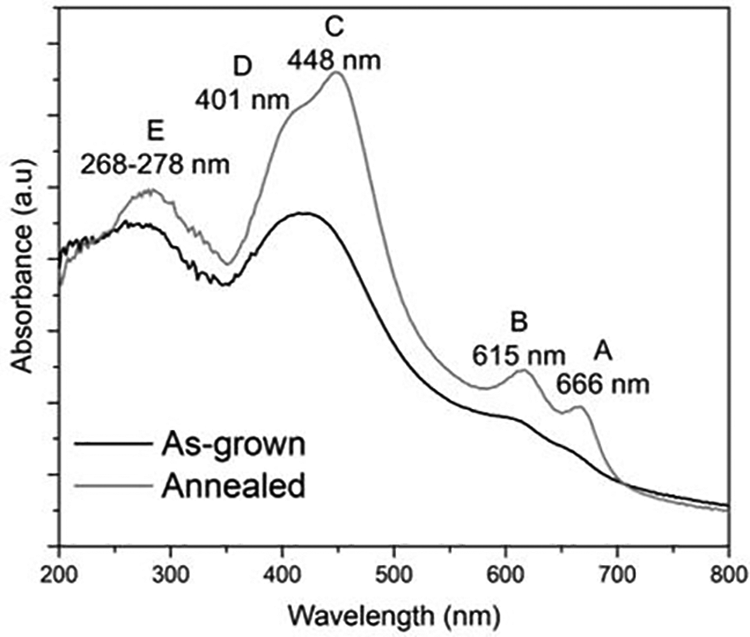
Absorbance spectra of the as-grown and annealed MoS2 samples. Labels A to E refer to the optical transition in MoS2.
FL MoS2 FET was fabricated using the annealed sample. Figure 5(a) shows the output curve (drain current (I ds) versus drain voltage (V d)) where V d was swept from 0 V to 5 V and the gate voltage (V g) was varied from −4 V to 10 V at an interval of 2 V. No hysteresis was observed in the curve. The results show that I ds increases with the increase of V g, indicating that the transistor is n-type. It was proposed that the origin of n-type operation in MoS2 is due to S vacancies in the structure. 34 The presence of S vacancies in our sample could be due to (i) incomplete sulfurization and/or (ii) desorption of S during annealing. In this case, incomplete sulfurization is unlikely because sulfurization was performed at high pressure and long period of time (∼125 kPa for 1 h). Our previous XPS study also shown that the as-grown MoS2 film consists of excess S with S: Mo ratio of >2. 23 It is possible that S vacancies were formed during annealing even though preventive steps (by using a covering plate) were already taken.

(a) Output characteristics of MoS2 FET when V g is increased from −4 V to 10 V. (b) Transfer characteristics of MoS2 FET, in linear (left) and log (right) scale. V d is set at 10 V.
Figure 5(b) shows the transfer curve, where V g was swept from −5 V to 10 V and V d was fixed at 10 V. Electron mobility at saturation (μsat) can be calculated from the following equation 23

where W and L are the width (400 μm) and length (100 μm) of the channel, Ci is the capacitance per unit area of the gate dielectric (25 nm Al2O3) of 1.94 × 10⁻⁷ Fcm−2, and V th is the threshold voltage. Based on the |I ds|1/2 versus V g plot at V d = 10 V, the extracted value of µsat is 0.21 cm2V−1s−1 and V th is 0.72 V. The estimated on/off ratio is 1.3 × 10². The low threshold voltage obtained from the FL MoS2 thin film FET may be due to good interface between MoS2 and Al2O3 (gate dielectric). 20 The electron mobility of our device is comparable to previously reported FL MoS2 FET synthesized by multi-step CVD which is in the range of ∼0.2 cm2V−1s−1. 20,23 Even though the electron mobility of our device is lower than mechanically exfoliated FL MoS2 FET (∼70 cm2V−1s−1), multi-step CVD can yield a larger area and scalable MoS2 thin film than mechanical exfoliation which yields random shapes and sizes of MoS2 flakes.
Conclusion
In conclusion, the effect of post-annealing on the structural and optical properties of MoS2 thin films was investigated. Raman and XRD analyses showed that the crystallinity of MoS2 thin films improved significantly after annealing and the absorbance spectra showed more prominent A, B, C, and D exciton peaks. This work shows the importance of post-annealing process in multi-step CVD to obtain a high-quality FL MoS2 thin films.
Footnotes
Declaration of conflicting interests
The author(s) declared no potential conflicts of interest with respect to the research, authorship, and/or publication of this article.
Funding
The author(s) disclosed receipt of the following financial support for the research, authorship, and/or publication of this article: This work was supported by the Fundamental Research Grant Scheme (FRGS/1/2019/STG07/UKM/02/6) from the Ministry of Education Malaysia. Part of this work was supported by Research Grant No GUP-2020-072 from Universiti Kebangsaan Malaysia.