
Abstract
In this article, we report modeling, simulation, and analysis of shifting 2D photonic crystal cavity side holes in GaN-AlN-sapphire layered structure. The design was simulated with Lumerical finite-difference time-domain. A lattice constant a, 157 nm, and a hole diameter d, 106 nm, were used in the design. The cavities are based on L3, which we demonstrated by simply shifting two holes away from a line cavity with distances of 132, 142, and 152 nm, respectively. The highest quality factor, Q, value achieved is 2.25 × 10⁴ at 152-nm cavity distance.
Introduction
Photonic crystal (PhC) has garnered more research attention recently because of the capability in controlling the propagation of light. PhC has been shown to modify and even eliminate the density of electromagnetic (EM) states inside the crystal. 1,2 The photonic bandgap (PBG) that limit the propagation of light is very sensitive to the wavelength and angle of incident light in PhC 3 ; due to these drawbacks, the energy band of the semiconductor material of the light-emitting wave range must be located in the PBG. 4 There are three PhC configurations actively researched and those are one-dimensional (1D), two-dimensional (2D), and three-dimensional (3D), and each dimension has its specific applications and advantages on each other. The 2D PhC 5 –15 is quite popular in the demonstration of photon propagation in several applications, such as switches, optical filter, sensor, and cavity quantum electrodynamics. PhC has PBG due to its periodic dielectric structure and different frequency 16 and can be used in many applications, including the fabrication of lossless dielectric, mirrors, and resonant cavities for optical light. 17 Wide bandgap III-nitride semiconductor, such as gallium nitride (GaN), is well-known optoelectronic material for light-emitting diodes and laser application. 18,19 However, it has been recently determined as a potential material system for technologies, such as PhC-based circuits and applications. 20 –22 AlN as a buffer layer is significant for fabrication of GaN, which is in the previous study has reported that the growth of GaN was deposited on the AlN buffer layer. As well known, the lattice mismatch AlN buffer layer between GaN is 17%. Normally, a buffer layer has to be applied to reduce the strain on the epitaxial GaN layer, and the influence of both materials (GaN and AlN) may increase the high quality (Q) factor of PhC cavities. 23 –26
The finite-difference time-domain (FDTD) method 27 is a numerical method used to solve the Maxwell equation and simulate a space of theoretically infinite. Time-domain computations allow for an unambiguous characterization of important properties of microcavities, such as bandgap features, resonant-defect mode dynamics, and far-field pattern properties of crystal modes. The results have frequently been interpreted by the use of fast Fourier transform analysis and filtering techniques. 6 It has been widely used to study EM properties of arbitrary dielectric structure and this method can calculate the band structure in periodic structure. However, the ability to get the high Q factor value for microcavity device structures is characteristically specified as the ratio Q/V is Purcell factor (F p), where Q is the factor and confinement of light in small modal volume (V) and EM resonant modes. 28,29,30 The higher Q factor as the longer cavities or the field at the edge were given when scattering happens is decreased while V leads to a small for the Q/V ratio.
Materials and methods
Top view of GaN on sapphire which is the structure in L3 type defect (three missing holes) in a line with triangular lattice and the position of hole displacement in the L3 cavity are shown in Figure 1. The structure from top to bottom is composed of GaN thin film with a thickness of 500 nm (refractive index of 2.5), 100 nm AlN as buffer layer (refractive index of 2.15), and bulk sapphire substrate (refractive index of 1.7), as shown in Figure 2. In this design of PhC, we choose the circular shape hole. The circular shape is better than the square shape of PhC because the circular shape is great and can easily control the wavelength. However, the square shape will abrupt changes in the flow of light in the structure and light will get reflected and scattered to give low transmission. 24

Hole shift of an L3 defect cavity in a 2D triangular lattice PhC.
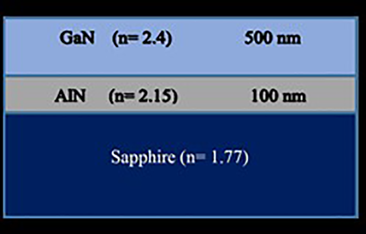
Side view of the device.
The 2D PhC is designed with circular holes etched in the GaN layer having a triangular lattice, 24 where the hole diameter d is 106 nm and the lattice constant a is 157 nm while the hole displacement was shifted from hole B to A. We varied the design with three different hole displacement values at a time for a lattice constant between A and B (132, 142, and 152 nm). This results in changing the cavity geometry, thus affecting the L3 cavity distance. There are many methods, such as transfer matrix method, FDTD method, plane wave expansion method, and finite-element method (FEM) available to analyze the dispersion behavior and transmission spectra of PhC. FDTD methods with respect to their performance and demand to analyze the PhC-based devices to calculate both transmission and field distribution are based on the numerical solution of Maxwell’s equations and also solvers confirmed the computed profiles and Q-factors and V of the cavity modes. Simulations using finite-difference time-domain (FDTD) and FEM solvers confirmed the computed profiles and Q-factors and V of the cavity modes. So, the structure is designed by 2D FDTD Lumerical solution to calculate Q and V of the fundamental transverse electric (TE) cavity mode.
Results and discussion
In this article, we have investigated the shift of the hole of triangular lattice PhC structure using the FDTD method. The simulated structure was the three missing holes or L3 cavity adjacent lattice at the center of the design, which we later shifted the hole, as shown in Figure 1. The shifted hole with shifted lattice constant at the center as 132, 142, and 152 nm. FDTD method was chosen since it is based on Maxwell’s curl equations for reflection, refraction, and diffraction. Maxwell equations in FDTD are solved based on electric (E) and magnetic (H) field.
The 2D simulation has been used for quick simulation respond. To get as accurate as 3D simulation, the effective index for the whole stack has been used in the simulation setup. TE mode is shown in Figure 3, where PhC can confine light mode perfectly created by defects in these layers that strongly simulate the TE mode created by corresponding defect in 2D. So, λ/2n eff, where λ is the wavelength and n eff is the effective refractive index ∼2.36.

The light confinement for that shows minimum loss transmission for TE mode light transmission was confined in the cavity of the structure. TE: transverse electric.
Figure 4 shows the stop-band PBG, which is the forbidden region and in between the wavelengths of 400–520 nm in blue to green region without any cavity. We observed three sharp resonance peaks in the middle of stop-band with the removal of three holes (L3).

The 2D FDTD simulation result 2D FDTD for stop-band without cavities.
Figure 5 shows the graphs of resonance transmission for a hole displacement at 132, 142, and 152 nm, where there are three sharp resonances, respectively. The lattice constant is defined as the distance of the cavity while the edge of the cavity was shifted to reduce the leaky component responsible for radiation losses as much as possible and thus strengthen the optical confinement. As expected, it can be deduced that the transmission decreases as the lattice constant increases. The graph in Figure 4 shows the transmission dependence of the hole displacement of the width cavity. From Lumerical FDTD simulation, an input with a value of 1 is applied for guiding light in a medium. By applying to a light-guiding device structure, a lossless device will produce a 100% output (which is 1 without any reflectance). The 30% of light has been measured at the output and due to the adequate frequency points set, some of the frequency maybe skipped in simulation hence the lower transmission. And if the transmission is really low after fabrication, an amplifier can be used to amplify the signal for real device applications. The L3 cavity, consisting of three missing holes in a triangular lattice PhC, has an additional parameter d to tune the condition of position for the confinement and to give a high-quality factor values.

Transmission to resonance peak intensity for shifted hole (a) 132 nm, (b) 142 nm, and (c) 152 nm.
Figure 6 shows the value of Q factor for the three peaks, which refer to the graph in Figure 5, respectively. The Q factor is also determined by the reflection loss at the interface between the internal and external of the cavity. The high Q of this design based on the FDTD method resulting in Q is 2.25 × 10⁴ at a resonance wavelength of 456 nm. This high Q cavity design will be fabricated for experimental characterization in the future.

The change of the Q factor with shifted hole.
Purcell factor is the emission rate enhancement of a strong light-matter inside a cavity or resonator for high Q/V with most PhC applications. The high Q factor measured by the Purcell factor is given by

where (λ/n) is the wavelength within the cavity material of refractive index, n, and Q and V are the quality factor and mode volume of the cavity, respectively. So, this is giving a Purcell factor of ∼104, which is the Q factor of 2.25 × 10⁴ and mode volume of 0.17 (λ/n) 3 . However, F P for lattice constant 132 and 142 nm are ∼103 and mode volume of 0.48 (λ/n) 3 and 0.53 (λ/n) 3 , respectively. In short, our goal is to design a high Q and low V mode using FDTD solutions.
Figure 7 showed the result of electric field at 152 nm hole shifted, where the light is confined in the cavity. The electric field profile inside a cavity can be indicated by function F(x) multiplied by the sinusoidal light wave of wavelength λ. To attain strong confinement and a high Q, the main condition is to satisfy a Bragg reflection that can produce an electric field profile inside the cavity, such as a Gaussian.

Electric field at hole shift 152 nm.
The electric field profile, as shown in Figure 6, follows a Gaussian distribution and the mode is gently confined in the defect region, which plays a major role in the increase of Q factor. Figure 6 shows the calculated electric distribution of the fundamental cavity mode for the structure representation of the |Ey |-field through the center of the cavity in the y and x planes. So, it is assumed that the electric field is strongly confined in the cavity. Light confined in a very small cavity consists of plane wave components with wave vectors (k) of various magnitudes (k) and directions to the localization of light.
Conclusions
In summary, we have determined high Q L3 PhC on GaN-sapphire, which we demonstrated by simply shifting two holes away from a line cavity with cavity distance of 132, 142, and 152 nm, respectively, to obtain the smallest mode volume with maximized Purcell factor. This proves that introducing cavity in GaN on sapphire will give high Q factor. The Q factor as high as 2.25 × 10⁴ has been observed in 2D shifted hole for lattice constant 152 nm compared to lattice constant shift at 132 and 142 nm. So, from FDTD calculation, we have obtained the Purcell factor of ∼104, in which Q of 2.25 × 10⁴ and mode volume of 0.17 (λ/n) 3 were calculated. The L3 design is a point defect cavity, which is suitable for strong light–matter interaction for dense integration in 2D circuit. Our design with high Q and 30% transmission is a great promise for lab-on-chip laser fluorescence and will have a high potential future for blue-light integration circuit applications.
Footnotes
Acknowledgment
The authors would like to thank UKM for supporting this project using grant GUP-2019-070.
Declaration of conflicting interests
The author(s) declared no potential conflicts of interest with respect to the research, authorship, and/or publication of this article.
Funding
The author(s) disclosed receipt of the following financial support for the research, authorship, and/or publication of this article: The authors received financial support of this article using grant GUP-2019-070.