
Abstract
Wide bandgap semiconductor ZnO, GaN and InN nanowires have displayed the ability to detect many types of gases and biological and chemical species of interest. In this review, we give some recent examples of using these nanowires for applications in pH sensing, glucose detection and hydrogen detection at ppm levels. The wide bandgap materials offer advantages in terms of sensing because of their tolerance to high temperatures, environmental stability and the fact that they are usually piezoelectric. They are also readily integrated with wireless communication circuitry for data transmission.
1. Introduction
The explosion of interest in nanoscience, coupled with growing demand for reliable, low-power chemical sensors for a wide variety of industrial applications, has led to a surge in the development of nanostructured materials for gas detection [1–5]. One-dimensional (1D) nanostructures, such as nanowires, nanorods and nanobelts, are particularly suited for chemical sensing due to their large surface-to-volume ratio [6–11]. In terms of material selection, wide band-gap semiconductors are ideal for gas sensing, having numerous advantageous properties, including an ability to operate at high temperatures (or alternatively, a low leakage current at room temperature), radiation and environmental stability, and mechanical robustness. The literature of more than a decade of research indicates an improvement in consistent growth methods and the potential for the immediate industrial use of 1D semiconductor nanostructures. Specific semiconductor materials including III-nitrides such as GaN [12–13] and InN [14–16], metal oxides including ZnO and SnO2 [17–18], and high-temperature materials such as SiC [19] have seen the greatest interest for chemical gas sensing applications, chiefly for the detection of H2, O2, NH3 and ethanol. There is also interest in applying these to biomarker detection [21–30].
There is a strong need for mobile, accurate, low power sensors that can be used in applications such as personal health monitoring, security, perimeter defence, food spoilage, the monitoring of nuclear materials and gas leaks. Currently, many of these applications are monitored by lab-based methods, such as enzyme-linked immunosorbent assay (ELISA), particle-based flow cytometric assays or electrochemical measurements. These methods have impressive sensitivity and reproducibility. However, many of the applications mentioned above would benefit from the ability to have sensing capabilities in a broader range of environments. To move these out of lab environment requires miniaturization and new approaches to solving power consumption and hand-held capability. In particular, it would be good to have a wireless capability for sending sensor data to a remote monitoring site and also to miniaturize the sensors so as to allow for truly mobile or long-term remote monitoring. The techniques mentioned above all have significant limitations in terms of using them outside of controlled lab environments, both in terms of the size of the components and power requirements. For long-term monitoring applications, self-powering techniques must be developed as well as power control methods that minimize power consumption. It is also desirable to minimize the sensor weight and size requirements and to produce a sensor that is consistent with other hand-held devices. Structures such as nanowires are attractive candidates because of their ease and the low cost of synthesis, low power consumption and compatibility with existing semiconductor components.
Semiconductor-based sensors can be fabricated using mature techniques from the Si chip industry and/or novel nanotechnology approaches. Sensors in these harsh environments must selectively detect hydrogen at room temperature or below while using minimum power. Several groups have already demonstrated the application of nitride and oxide semiconductor nanostructures for exclusive H2 sensing using carbon nanotubes (CNTs) and ZnO. Several issues must still be addressed, however, including quantifying sensitivity, improving detection limits at room temperature, establishing the reproducibility and stability of the sensors and reducing power consumption. Materials such as ZnO show sensitivity to environmental exposure, particularly in terms of forming surface conducting layers in the presence of oxygen or water vapour exposure. Thus, the issue of surface passivation and encapsulation for the sensors is another area that must be developed. This is not expected to be a long-term impediment, since polymer-based organic electronic and display materials have a similar issue which has been mitigated to a large extent by employing appropriate methods to limit the exposure of the material to ambient conditions.
There are many potential applications for wide bandgap semiconductor nanowire devices because of their improved carrier confinement over their thin film counterparts. For GaN nanowires, there are possible applications in low power and high density field-effect transistors (FETs), solar cells, terahertz emitters and UV detectors. The high surface-to-volume ratio of nanowires means that if their surfaces are sensitive to external stimuli or can be functionalized to be sensitive to specific chemicals or biogens, then they are likely to be attractive for gas and chemical sensor arrays. ZnO is a piezoelectric, transparent, wide bandgap semiconductor used in surface acoustic wave devices. The bandgap can be increased by Mg doping. ZnO has been effectively used as a gas sensor material based on the near-surface modification of charge distribution with certain surface-absorbed species. In addition, it is attractive for biosensors given that Zn and Mg are essential elements for neurotransmitter production and enzyme functionality.
In this review, we discuss the progress of nitride and oxide semiconductor nanostructures for nanoelectronic devices and for chemical and gas sensing, specifically for hydrogen. The functionalizing of the surface with oxides, polymers and nitrides is also useful in enhancing the detection sensitivity for gases and ionic solutions. The wide bandgaps of these materials make them ideal for solar-blind UV detection, which can be used for detecting fluorescence from biotoxins. The use of enzymes or adsorbed antibody layers on the semiconductor surface leads to the highly specific detection of a broad range of antigens of interest in the medical and homeland security fields. The use of catalyst metal coatings on GaN, InN and ZnO nanowires has been found to greatly enhance the detection sensitivity for hydrogen. Pt- and Pd-coated GaN nanowires biased at small voltages show large changes in currents upon exposure to H2 gas at concentrations within the ppm range. Improvements in growth techniques for InN nanostructures have produced nanobelts and nanorods capable of hydrogen detection down to 20 ppm after catalyst coating. Functionalized ZnO nanorods were also investigated for hydrogen detection, but did not generate a relative response as high as that for the nitride-based sensors.
2. Gallium Nitride (GaN) nanostructure-based sensors
GaN's use as a chemical sensor is well-documented [26–34]. GaN has a high breakdown field, can operate at high temperatures in excess of 400

Dissociated hydrogen causes a change in the channel and conductance change of the nanowire by altering the zero-bias depletion depth.
While reports on nanostructured GaN gas sensors are increasing, the difficulty in achieving reproducible material has limited their number in the literature. The various growth techniques used for nanowire synthesis are still a long way from standardization and, as a result, have produced a wide range of 1D GaN nanostructures of varying crystal quality. The current growth methods of 1D nanostructured GaN include arc-discharge, laser-assisted catalytic growth, the direct reaction of a mixture in a tube furnace and, most recently, chemical vapour deposition (CVD) from Ga-containing precursors and NH3 on catalyst-coated substrates.
The use of CVD for 1D nanostructure preparation is based on the vapour-liquid-solid (VLS) growth mechanism in which solid GaN nanowires nucleate/precipitate on catalyst nanoparticles of (typically) In, Au, Fe, Ni or Co at the substrate surface. Although a minimal nanowire diameter is directly related to device sensing capability and the desired optical characteristics, the diameter is limited by the minimum size of catalytic metal beading at the surface. Previous reports have demonstrated the growth of GaN nanowires with minimum diameters of 6 nm using metal complexes instead of elemental metals as surface catalysts for deposition. GaN nanowire growth by CVD has issues with the high melting point of Ga-precursors, which may encourage Ga oxidation with residual oxygen in the CVD chamber. A hydrogen gas co-flow with NH3 prevents the oxidation of GaN nanowires upon deposition.
For our work, a growth substrate for GaN nanowire deposition was prepared by e-beam, evaporating 15 Å gold onto (100) Si with 100 nm thermally grown oxide. GaN nanowires were deposited by the reaction of liquid gallium and NH3 in a 1-in. atmospheric quartz tube furnace. The substrate was heated to 850°C and annealed for 15 min under Ar ambient in order to form discrete Au nanoparticles on the surface. Growth was performed at 850°C for 2 −5 h under a flow rate of 15–17 sccm NH3 and 300 sccm H2. The typical length of the produced GaN nanowires was 2–10 μm. The addition of the metal catalyst makes a large difference to the sensitivity of the sensors, as shown in Figure 1. The inset of Figure 2 (top) shows the morphology of as-grown GaN nanowires before functionalization. The characterization of the nanowires showed a high-quality, single-crystal wurtzite structure [12,13]. It turns out to be surprisingly straightforward to achieve good crystal quality nanowires using a variety of different synthesis methods. For systems such as ZnO, it is also possible to grow the nanowires at temperatures around room temperature, which makes them compatible with a large variety of substrates, including plastic, tape and even paper. The ability to use arbitrary substrates makes this a versatile approach.
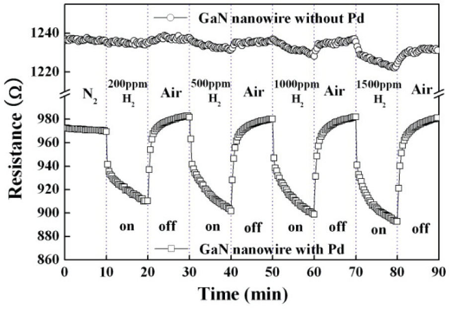
Change in resistance of GaN nanowires, either with or without Pd coatings, as a function of gas ambient switched in and out of the test chamber. (Reprinted with permission from Ref.110, W. Lim, J.S. Wright, B.P. Gila, J.L. Johnson, A. Ural, T. Anderson, F. Ren and S.J. Pearton, Appl. Phys. Lett. 93, 072110 (2008). Copyright American Institute of Physics).
Relative responses of metal coated GaN nanowires to varying hydrogen concentrations at room temperature. Top) Pt-coating. Bottom) Pd-coating. Insets show GaN nanowires before (as-grown; top) and after Pt deposition (bottom).
Often, the addition of a functional catalytic layer to the sensing substrate surface is a crucial step in the effectiveness of wide band-gap sensors. Catalytic functional layers work to dissociate molecular compounds into atomic components which then bond easily onto the sensor interface; for example, the catalytic dissociation of H2 into 2H by Pt metal. Although this mechanism of dissociation by functional layers for H2 sensing is well-understood, the material choice of the functional layer is still disputed for GaN. Both Pt and Pd have generally been accepted as choice metals for functional coatings on nitride-based sensors; however, there have been few reports comparing the two metal functionalities. We would emphasize that the metal catalyst layer is discontinuous and there is no current path from the contacts to the metal. This fact rules out a change in the conductivity of the metal due to the storage of hydrogen as contributing to the sensor signal.
Our GaN nanowires were functionalized for H2 detection with thin Pt or Pd films (∼100 Å thick) deposited by sputtering. Deposited functional layers were checked for discontinuity at the surface by SEM. The morphology of functionalized GaN nanowires is shown in the inset of Figure 2. Al/Pt/Au Ohmic electrodes contacting both ends of multiple nanowires were deposited by sputtering using a shadow mask. Au wires were bonded to the contact pad for current-voltage (I-V) measurements performed at 25–150°C in H2 at varying concentration (10–3000 ppm) in N2 ambience. Note that no underlying thin film of GaN was observed for the conditions used to grow the tested nanowires.
2.1 Hydrogen Detection Using Gallium Nitride Nanostructures
Figure 3 shows the time-dependant relative response (ΔR/R) of the metal-coated GaN nanowire sensors as the gas ambient is switched from air to varying hydrogen concentrations in N2 ambience and then back to air. As shown from the difference in Figure 3 (top) and 3 (bottom), Pd-coated GaN nanowires produced a higher relative response over the same nanowires as when functionalized with Pt. Comparatively, Pd-coated GaN nanowires showed relative responses of ∼7.4% at 200 ppm up to ∼9.1% at 1500 ppm. The relative responses of Pt-coated nanowires were ∼1.65% at 200 ppm up to ∼1.85% at 2000 ppm. Uncoated nanowires had little or no effective response to changes in measurement ambient, i.e., they showed no significant detection of hydrogen.
Relative responses of Pt-coated InN nanobelts to varying hydrogen concentrations at room temperature.
It is clear that both Pt and Pd are effective in their catalytic dissociation of molecular H2 into atomic hydrogen. Although it takes >5 min for hydrogen to saturate relative to the response of Pt-coated nanowires, the initial resistance change is noticed in less than 2 seconds of H2 exposure for both metal-coated nanowire sensors. This suggests that the diffusion of hydrogen through the metal coating is not the limiting factor in the time response of the sensors, but rather that it is limited by the mass transport of gas into the enclosure. This factor was confirmed by altering the H2 introduction rate into the test chamber. While the resistance change depended on hydrogen gas concentration, variations to change upon hydrogen exposure were small at H2 concentrations above 800 ppm. The rate of resistance change decreases as the nanowire surface becomes saturated with hydrogen in all cases. In contrast to previous functionalized GaN nanowire sensors, these devices exhibit near perfect reversibility, as shown by the near complete recovery of the original current response in the air upon the removal of hydrogen. The repeatable detective ability of these sensors over previous one-use-only functionalized devices is promising for long-term applications.
Although the detection mechanism for hydrogen on GaN nanowires is still not fully understood, previous suggestions for sensing include the desorption of adsorbed hydrogen at the surface and grain boundaries (in polycrystalline material), an exchange of charges between absorbed gas species and the interface leading to a change in the depletion depth, or else changes to the conduction at the surface by gas adsorption and desorption. Hydrogen gas sensing on functionalized GaN nano-surfaces has previously been explained as follows. As the sensor surface is exposed to hydrogen gas, hydrogen molecules are catalytically dissociated on the functional metal surface into atomic hydrogen. These hydrogen atoms are absorbed on to the metal surface and subsequently diffuse through the nano-particulate metal coating until they are adsorbed at the metal/GaN interface. Hydrogen atoms reaching the GaN surface form a dipole layer at the interface, causing a measurable change in the electrical field across the depletion region directly below the GaN surface. This change in the depletion layer leads to a modulation of the barrier height and a difference in the measured forward- and reverse- bias currents.
The activation energy calculated for both GaN nanowire sensors was higher than expected for a typical H diffusion process in Pt, Pd or GaN. As such, this energy was attributed to the chemiadsorption of H to the metal/semiconductor interface. The calculated values were ∼7.3 kcal mol−1 for Pt-coated GaN and ∼2.2 kcal mol−1 for Pd-coated GaN. Both Pt- and Pd-coated GaN nanowires showed no change in resistance upon exposure to other measurement ambiences, including O2, CO2, NH3 and C2H6.
3. Indium Nitride Nanostructure-based Sensors
InN has received significant attention recently due to its narrow direct bandgap (0.7–0.8 eV) and superior electronic transport characteristics. This, combined with its easily integrated structure with other nitrides, including GaN and AlN, makes it a promising material for high efficiency IR emitters, detectors and solar cells, as well as for use in high frequency electronic devices. Though the research is increasing, reports on the growth, properties and applications of InN nanostructures remain in their infancy.
The growth of InN nanostructures by conventional metal organic chemical vapour deposition (MOCVD) has met with difficulty because of the low thermal decomposition temperature of InN (< ∼600
For the development of InN nanostructured sensors, the growth of InN nanobelts was performed by MOCVD on Si substrates using TMIn and NH3 as In and N sources, respectively, while nitrogen was used as the carrier gas. The nucleation sites for the catalyst-driven growth of the nanobelts were formed by depositing 2 nm of Au film on SiNx-coated Si substrates by direct current sputtering. InN nanobelts were synthesized at 500°C and 5 Torr pressure for 2 hours. The nanobelts exhibited well-defined side facets with typical lengths of ∼1μm. A ∼7 nm-thick layer of Pd was sputter-deposited onto some of the nanobelts. A shadow mask was used to pattern non-alloyed, rf-sputtered Ti/Al/Pt/Au Ohmic contacts on the InN nanobelts with a contact separation of ∼50 μm. Au wires were bonded to the contact pads for device packaging. The InN nanobelts sensors were exposed to different H2 concentrations (100–1000 ppm H2 in N2 ambient) at 25–130°C. The sensor response to high concentrations of CO2, C2H6, NH3 and O2 (all in N2 ambient) was also examined.
3.1 Hydrogen detection using Indium Nitride nanostructures
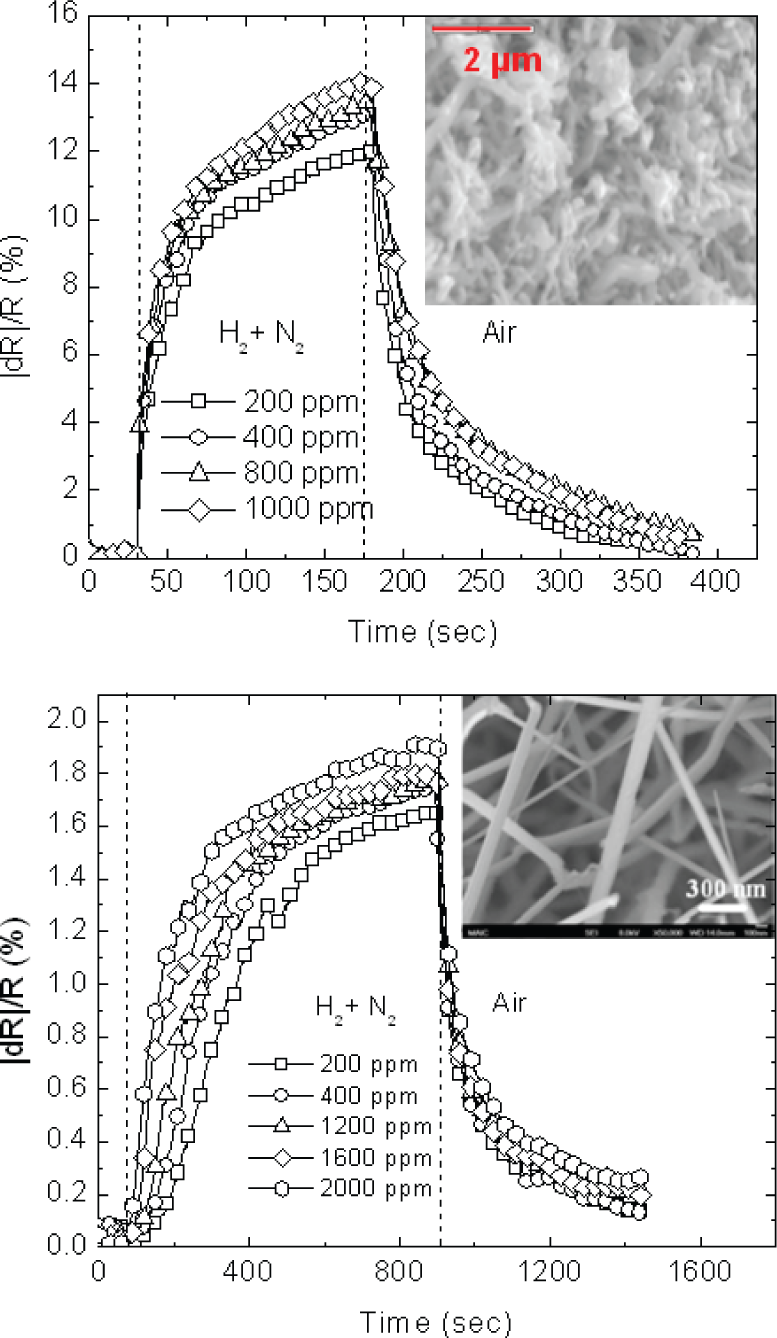
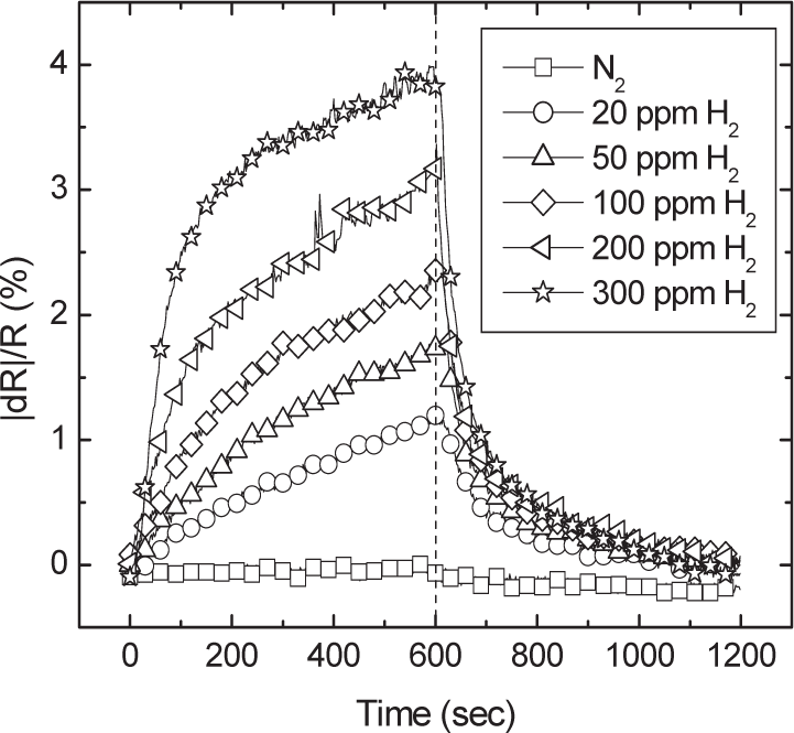
The addition of Pt or Pd metal onto InN nanobelts produced a strong response to H2 as compared with no detectable change in current for uncoated nanobelts under the same gas concentration. Pd-coated InN nanobelts detected hydrogen down to tens of ppm concentration levels with relative responses of ∼1.2% at 20 ppm and up to ∼4% at 300 ppm at room temperature, as shown in Figure 4. The resistance change increased with the measurement temperature from 3.1% at 200 ppm and room temperature to 4.5% and 5.6% and 90°C and 150°C, respectively. As with GaN nanowires, the increase in resistance change is a result of the increase in the catalytic dissociation rate of molecular hydrogen.

Relative responses of Pd-coated InN nanobelts to varying hydrogen concentrations at 130
The relative response of Pd-coated InN nanobelts was at least 30% larger for all temperatures in comparison with Pt-coated InN nanobelt hydrogen sensors. With Pd functionalization, the InN sensor detected hydrogen down to 100 ppm concentration levels (the equipment limit for this experiment), with a relative response of ∼8% at 100 ppm and ∼9.5% at 1000 ppm after a 5 minute exposure. The initial current response recovered ∼50% of the initial value within 10 minutes of the removal of the hydrogen from the ambience. This was slower than previous reports using Pt-coated nanobelts and could be due to Pd having a greater affinity for hydrogen.
The activation energy for H detection on both Pt- and Pd-coated InN nanobelts was calculated from the slope of the Arrhenius plot of natural log (dR/dt) versus 1/T. Pd-coated nanobelts were found to have an activation energy of 0.097 eV, whereas Pt-coated nanobelts had an energy of 0.12 eV. These values are low but still larger than those expected for a typical hydrogen diffusion in InN, Pt or Pd. Thus, and as with the results found for functionalized GaN nanowire hydrogen sensors, the dominant sensing mechanism is likely to be the chemisorption of H to the metal-nitride interface.
The utility of InN nanorods for hydrogen detection was also investigated. InN nanorods were grown on polished c-Al2O3 substrates by H-MOVPE. With this method, TMIn was reacted with HCl to form chlorinated indium. This was then combined with NH3 to form InN on the substrate downstream. The source zone temperature was kept below 300°C to prevent TMIn dissociation before reaction with HC1. Growth was completed at atmospheric pressure in N2 ambient in a temperature range between 600–650°C at a N/In mole ratio of 250 and a HC1/TMIn inlet mole ratio of 4 to 5. Finally, InN nanorods were functionalized with a thin, discontinuous Pt-film (∼100Å) by sputtering.
Glancing Incidence X-Ray Diffraction (GIXD) scans of the InN nanostructures are shown in Figure 5. Since the orientation of each nanostructure was largely random, multiple wurtzite InN peaks were observed for both InN nanobelts and InN nanorods. Of note here are the larger, sharper peaks for the nanorods as against those for the nanobelts. This difference in the XRD profile may be attributed to a thicker, denser nanostructured surface, and is supported by the variation in surface morphology as shown in the SEM inset photos. The nanorods are typically larger, longer and denser over the substrate surface.
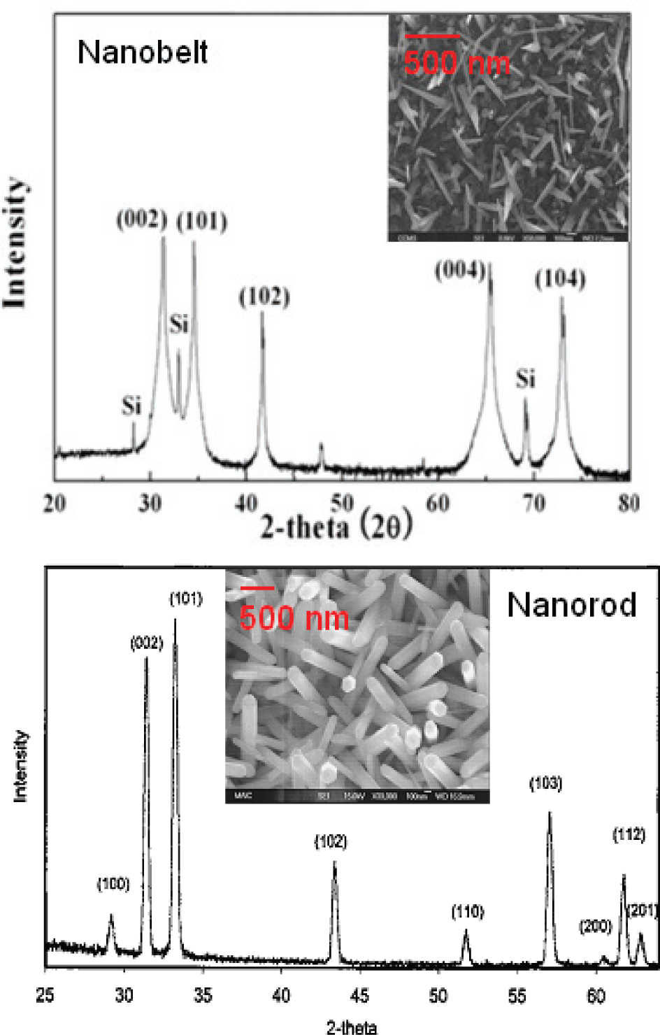
GIXD 2θ scan of InN nanomaterials. A) InN nanobelts on SiNX-coated Si. B) InN nanorods on c-Al2O3. Insets show SEM micrographs of the respective deposited InN nanomaterials.
The higher quality of these InN nanorods (as compared with the previously discussed InN nanobelts) results in a larger relative response upon exposure to hydrogen. Figure 6 shows the relative resistance change of the Pt-coated multiple InN nanorods upon hydrogen exposure. 100 ppm H2 in N2 ambience produced a relative response of ∼10%, while 250 ppm H2 gave a response of ∼12%. Unlike the immediate response of the InN nanobelts to hydrogen gas, however, the initial change in the resistance of InN nanorods upon hydrogen exposure was quite slow, taking up to five minutes exposure before exhibiting a current response. This slower response could be due to the Pt functionalization layer being covered with native oxide, which is removed by exposure to hydrogen. The higher surface density of the nanorods as compared with the previous nanobelts may also inhibit an immediate reaction to hydrogen exposure by the reduction of the nanostructure surface area. It is certainly true that producing higher quality nanostructures mitigates the effects of defects in the bulk or on the surface to the sensing response. It appears that many of the initial results in the literature concerning the gas sensing properties of nitride and oxide nanorods have been dominated by surface trapping/detrapping phenomena rather than by the true intrinsic response of the material itself.

Relative responses of Pt-coated InN nanorods to varying hydrogen concentrations at room temperature. (Reprinted with permission from Ref.111, W. Lim, J.S. Wright, B.P. Gila, S.J. Pearton, F. Ren, W. Lai, L.C. Chen, M. Hu and K.H. Chen, Appl. Phys. Lett. 93, 202109 (2008). Copyright American Institute of Physics).
4. Zinc Oxide (ZnO) nanostructure-based sensors
There is a great deal of literature dedicated to the synthesis and characterization of various types of nanostructured ZnO morphologies. A review of the many forms of nano-sized ZnO, including nanobelts, -cages, - combs and -wires is provided by Wang [11]. This ease of nano-fabrication, combined with the high compatibility with Si-based microelectronics afforded to semiconducting metal oxides, makes ZnO a particularly interesting candidate for solid-state chemical gas sensing. ZnO is a chemically and thermally stable, inherently n-type semiconductor with a large exciton binding energy and wide bandgap. ZnO-based gas sensors have already been developed from thin films, nanoparticles and nanowires. Additionally, ZnO easily forms a heterostructure system with MgO and CdO over a limited miscibility range that is promising for blue/UV optoelectronics, transparent electronics and sensors.
4.1 Hydrogen detection using Zinc Oxide nanostructures
For our work, the site selective growth of ZnO nanorods was achieved by Molecular Beam Epitaxy (MBE) on Al2O3. The growth time was ∼2 h at 600°C, producing single crystal nanorods with a typical length of 2–10 Lim and having a diameter between 30–150 nm. Al/Ti/Au electrodes were deposited via e-beam with a separation distance of ∼3 μm. Finally, Au wires were bonded to the contact pads for I-V measurements performed at temperatures between 25–150°C in 10% H2 in N2 ambience. No current was measured through the discontinuous Au islands and no thin film of ZnO was observed with the grown conditions of nanorods. In some cases, nanorods were functionalized using Pd, Pt, Au, Ni, Ag or Ti discontinuous thin films (∼100 Å thick) deposited by sputtering.
Although there was no detectable change in current upon H2 exposure at room temperature, ZnO nanorods did reflect changes in current, beginning at ∼112°C. While change in current only approaches 16 nA at 200°C, these changes are readily detected by conventional ammeters; however, an on-chip heater would be needed for the practical application of ZnO nanorods for the detection of hydrogen. Nonetheless, these results show the possible capability of ZnO nanorods for use in hydrogen gas sensors without the deposition of an additional functional layer. In this case, the gas sensing mechanism is believed to derive from the desorption of absorbed surface oxygen and grain boundaries in poly-ZnO or else from changes in surface or grain boundary conduction by gas adsorption/ desorption. Since the nanowires are typically a single crystal, the latter effect is not likely to contribute. When detecting hydrogen with similar thin film rectifiers, the observed changes in current were consistent with changes in the near surface doping of the ZnO, suggesting the introduction of a shallow donor state via hydrogen adsorption. The nanorods also showed a strong photoresponse above bandgap UV light (366 nm). The quick photoresponse indicated that the changes in conductivity due to the injection of carriers was bulk-related and not due to surface effects.
As with to GaN and InN, previous reports have shown that the addition of metallic nanoparticles on the surface increases the detection sensitivity for H2. Accordingly, and as with the GaN nanowires and InN nanobelts, metal catalyst coatings were deposited to ZnO nanorods to increase the detection efficiency for hydrogen gas. Figure 9 shows the time dependence of the relative resistance change of metal-coated multiple ZnO nanorods with various metal functionalization layers upon exposure to 500 ppm H2. The measured bias voltage was 0.5V. Pt-coated nanorods exhibited a relative response of up to 8% at room temperature upon exposure to 500 ppm hydrogen concentration in N2 ambience. Unlike the results for the nitride-based nanostructures, this was a factor of two larger than obtained with Pd-coatings. The Pt-coated ZnO nanorods easily detected hydrogen down to 100 ppm (the experimental limit), with relative responses of 4% at this concentration after a 10 min exposure. All of the other metals' functional layers showed very little relative responses to hydrogen exposure (Figure 7).

Relative responses of ZnO nanorods to 500 ppm H2 using various metal functionalizations. (Reprinted with permission from Ref.89, Y.W. Heo, D.P. Norton, L.C. Tien, Y. Kwon, B.S. Kang, F. Ren, S.J. Pearton and J.R. LaRoche, Mat. Sci. Eng. R 47, 1 (2004). Copyright Elsevier).
SEM micrograph of ZnO nanowire and time dependence of photocurrent as the 366nm light source is modulated.

The SEM of an integrated microchannel across a ZnO nanorod contacted at both ends by Ohmic contacts. The conductance of the nanorod as a function of the pH of the solution which flowed across it is shown at the bottom of the figure.
Differences in the relative response to hydrogen exposure between Pt- and Pd-coated samples were suggested as coming from the catalytic properties of the metals. Pd has a higher permeability than Pt, but the solubility of H2 is larger in Pd. Additionally, bonding studies of H to Ni, Pt and Pd surfaces have shown that adsorption energy is lowest on Pt. As shown, however, the calculated activation energy for GaN nanowires and InN nanobelts was lower for Pd-coated samples rather than Pt. This is most likely due to the adsorption of hydrogen at an oxide interface between the nitride surface and the metal and not from the adsorption of hydrogen at the metal coating. The existence and importance of this oxide interface for hydrogen sensing on nitride-based semiconductors is well-documented. Because the hydrogen adsorption on the oxide side of a ZnO-based sensor would contribute to the creation of a shallow donor state, the sensing mechanism for hydrogen detection on metal coated ZnO nanostructures is probably different from that of GaN or InN.
Similar to nitride-based nanostructured sensors is the rapid, initial response of ZnO multiple nanorod sensors to hydrogen exposure. Effective nanorod resistance continues to change for >15 minute of exposure. This suggests that the chemisorption of hydrogen to the metal/ZnO interface is the rate-limiting step in conductance changes to the ZnO. The recovery of initial resistance upon the removal of hydrogen from the ambience was rapid (<20 sec). A calculated activation energy of 12 kJ/mole originated from the chemisorption of hydrogen onto the metal coating surface.
4.2 Other Zinc Oxide nanostructure-based applications
4.2.1 UV Photodetectors
The development of GaN-based UV detectors in the spectral range shorter than λ∼400 nm has attracted much interest recently because of their potential application in the detection of biological materials and for the defence industry. In the former case, the UV photons are used to excite fluorescence at UV wavelengths from biological materials of interest and this is detected by the photodetectors. Wide bandgap detectors are very useful in bio-warfare agent detection because some pathogenic biological molecules fluoresce in the UV spectral region.
The most common UV detectors are based on p-i-n Si photodiodes or UV-filtered photomultiplier tubes. The use of nitride semiconductor UV detectors has advantages in terms of more precise detection windows, lower background currents due to solar fluxes and a wider range of operating temperatures. Photodetectors that have no response for photons at wavelengths >290nm are called solar-blind and are useful in applications that need to detect UV photons in the presence of sunlight, such as flame sensors, missile detectors and aircraft detection. Si detectors have very poor solar-blind performance while wide bandgap systems offer improved speed and lower dark currents.
Currently, the most commonly used wide bandgap semiconductor system for UV detection is GaN/AlGaN. There is also interest in developing ZnO/ZnMgO nanowire UV detectors as a complementary technology for UV detection, with the following advantages relative to the nitrides.
The ZnO-based materials offer similar band-gaps to the nitrides, but can be grown at much lower temperatures on a wider range of substrates, including large area Si or cheap transparent materials, such as glass. The nanowires can be transferred to any substrate for integration with other sensors and are compatible with low temperature materials such as polymers.
The nanowire UV detectors operate at very low power levels compared with existing nitride UV detectors.
The fabrication approach developed previously for ZnO nanowire gas sensors allows for a simple, low-cost, single-step approach to realizing robust UV detectors.
ZnO nanowire UV detectors can be readily integrated with on-chip wireless circuits to provide data transmission to a central monitoring location. Thus, it is possible to have either single detectors or arrays of detectors that operate at very low-power levels and do not need constant monitoring by humans.
UV detectors have applications in space exploration in providing imaging and spectroscopic data of nearby galaxies. Because the universe is expanding, UV radiation emitted by distant galaxies is red-shifted and reaches our galaxy as visible or infrared radiation. Galaxies closer to the Milky Way can be analysed with UV radiation and comparisons can be made with visible and infrared images to ascertain how the universe formed and changes with time.
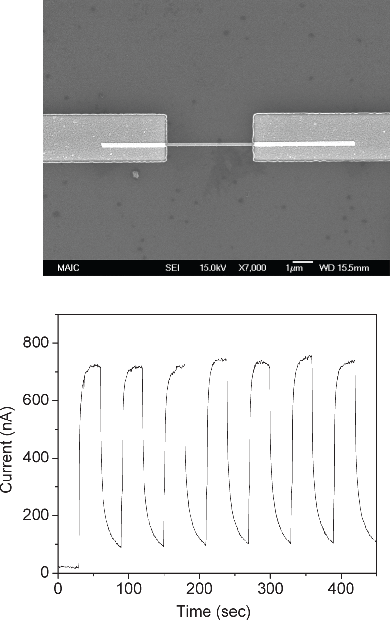
a) UV Photoresponse of Single ZnO Nanowires
ZnO nanowires grown by site-selective MBE were single crystals and typically conducting with a carrier density within the 1017-1018 cm−3 range. These nanowires can be removed by sonication from their original substrate and then transferred to arbitrary substrates, where they can be contacted at both ends by Al//Pt/Au Ohmic electrodes. The current-voltage and photoresponse characteristics were obtained both in the dark and with UV (254 or 366 nm) illumination. The current-voltage (I-V) characteristics are Ohmic under all conditions, with nanowire conductivity under UV exposure of 0.2 Ohm.cm. The photoresponse showed only a minor component, with long decay times (tens of seconds) thought to originate from surface states. Recent reports have shown the sensitivity of ZnO nanowires to the presence of oxygen in the measurement ambient and to UV illumination. The slow photoresponse of the nanowires was suggested as originating in the presence of surface states, which trapped electrons with release time constants from m.sec to hours. In sharp contrast to these results, we have demonstrated that the photoresponse characteristics of single ZnO nanowires grown by site selective Molecular Beam Epitaxy (MBE) have a relatively fast photoresponse and display electrical transport dominated by bulk conduction.
Figure 8 shows the change in current at a fixed bias of the nanowires in the dark and under illumination by 366 nm light. The conductivity is greatly increased as a result of the illumination, as evidenced by the higher current. No effect was observed for illumination for below bandgap light. Transport measurements show that the ideality factor of Pt Schottky diodes formed on those nanowires exhibiting an ideality factor of 1.1, which suggests that there is little recombination occurring in the nanowire. It also exhibits the excellent Ohmicity of the contacts to the nanowire, even at low bias. On blanket films of n-type ZnO with carrier concentration within the 1016 cm−3 range, we obtained a contact resistance of 3–5×10⁻⁵ Ohm.cm−2 for these contacts. In the case of ZnO nanowires made by thermal evaporation, the I-V characteristics were rectifying in the dark and only became Ohmic during above-bandgap illumination. The conductivity of the nanowire during illumination with 366 nm light was 0.2 Ohm.cm.
The photoresponse of the single ZnO nanowire at a bias of 0.25 V under pulsed illumination by a 366 nm wavelength Hg lamp in Figure 8 shows that the photoresponse is much faster than that reported for ZnO nanowires grown by thermal evaporation from ball- milled ZnO powders and is likely due to the reduced influence of the surface states seen in that material. The generally quoted mechanism for photoconduction is the creation of holes by illumination that discharge the negatively charged oxygen ions onto the nanowire surface with the de-trapping of electrons and transit to the electrodes. The recombination times in high quality ZnO measured by time-resolved photoluminescence are short - of the order of tens of ps - while the photoresponse measures the electron trapping time. There is also a direct correlation reported between the photoluminescence lifetime and the defect density in both bulk and epitaxial ZnO. In our nanowires, the electron trapping times are of the order of tens of seconds, and these trapping effects are only a small fraction of the total photoresponse recovery characteristic. Once again, we see an absence of the very long time constants for recovery seen in nanowires prepared by thermal evaporation.
4.2.2 pH measurement
There are a number of applications where an ability to determine the pH of a solution is desirable in order to understand the level of acidity or alkalinity. These include determining salinity levels in bodies of water, the industrial monitoring of sludges or run-off and, of course, blood in humans. Many oxides are sensitive to changes in the pH of solutions touching their surfaces through a change in surface conductivity. This makes materials such as ZnO, SnO2 and related compounds attractive for pH sensing applications.
Of particular interest in determining the ability of ZnO nanorods for acting as pH sensors is the need for a method of introducing the test solution in a controlled and reproducible fashion to the nanowire surface. This is usually accomplished by the use of a microchannel fabricated in a polymer. Small volumes of the solution can be introduced with a syringe autopipette. A typical geometry for the nanowire sensor and integrated microchannel and the conductance of the nanowire is shown in Figure 9. The measurements were performed both in the dark or under UV illumination (365 nm wavelength) at room temperature with the nanorod biased at a fixed voltage of 0.5 V
The nanorods showed a very strong photoresponse. The conductivity is greatly increased as a result of the illumination, as evidenced by the higher current. No effect was observed for illumination with below bandgap light. The adsorption of polar molecules on the surface of ZnO affects the surface potential and device characteristics.
The data in Figure 9 shows that the integrated microchannel/nanorod can indeed provide a sensitive measurement of pH over a range of at least 2 to 12. The sensitivity was independent of whether the experiments were carried out in the dark or under illumination. The slope of the conductance/pH plot was 8.5 nS/pH in the dark and 20nS/pH under illumination. The resolution of the measurements was typically ∼0.1 pH, which compares well with other methods for pH determination.
4.2.3 Biomedical Applications
AlGaN/GaN HEMTs can be used for measurements of pH in EBC and glucose, through the integration of the pH and glucose sensor onto a single chip and with the additional integration of the sensors into a portable, wireless package for remote monitoring applications. Figure 10 shows an optical microscopy image of an integrated pH and glucose sensor chip and cross-sectional schematics of the completed pH and glucose device. The gate dimension of the pH sensor device and glucose sensors was 20 × 50m2.
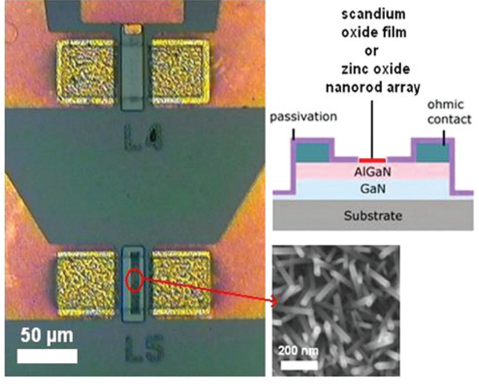
SEM image of an integrated pH and glucose sensor. The insets show a schematic cross-section of the pH sensor and an SEM of the ZnO nanorods grown in the gate region of the glucose sensor.
For the glucose detection, a highly dense array of 20–30 nm diameter and 2 μm tall ZnO nanorods was grown on the 20 × 50 μm2 gate area. The lower right inset in Figure 10 shows closer view of the ZnO nanorod arrays grown on the gate area. The total area of the ZnO was increased significantly with the ZnO nanorods. The ZnO nanorod matrix provides a microenvironment for immobilizing negatively charged GOx while retaining its bioactivity, and passes charges produced during the GOx and glucose interaction to the AlGaN/GaN HEMT The GOx solution was prepared with a concentration of 10 mg/mL in 10 mM phosphate buffer saline (pH value 7.4, Sigma Aldrich). After fabricating the device, a 5 μl GOx (∼100 U/mg Sigma Aldrich) solution was precisely introduced to the surface of the HEMT using a pico-litre plotter. The sensor chip was kept at 4°C in the solution for 48 hours for GOx immobilization on the ZnO nanorod arrays followed by extensive washing to remove the un-immobilized GOx.
To take advantage of the quick response (less than 1 sec) of the HEMT sensor a real-time exhaled breath condensate (EBC) collector is needed The amount of the EBC required to cover the HEMT sensing area is very small Each tidal breath contains around 3 μl of the EBC The contact angle of EBC on Sc2O3 has been measured as being less than 45° and it is reasonable to assume a perfect half sphere of an EBC droplet formed to cover the sensing area of the 4 × 50 μm2 gate area The volume of a half sphere with a diameter of 50 um is around 3 × 10⁻¹¹ litres Therefore 100 000 50 um diameter droplets of EBC can be formed from each tidal breath.
To condense 3 μl of water vapour only ∼ 7 J of energy need to be removed for each tidal breath which can easily be achieved with a thermal electric, module - a Peltier device The figure also shows a photograph and schematic of. the system for collecting the EBC The AlGaN/GaN HEMT sensor is directly mounted on the top of the Peltier unit (TB-8-0 45-13 HT 232 Kryotherm) which can be cooled to precise temperature, s by applying known voltages and currents to the unit During our measurements the hotter plate of the Peltier unit was kept at 21°C and the colder plate was kept at 7°C by applying a bias of 07 V at 02 A The sensor takes less than 2 sec to reach thermal equilibrium with the Peltier unit This allows the exhaled breath to immediately condense on the gate region of the HEMT sensor.
The use of Peltier cooling allows for a compact and low power approach to building the sensor unit. These units are inexpensive and very reliable, and can be used to control the amount of vapour condensation onto the sensor gate area. This might also be used in future to selectively control the condensation of particular gases in a mixture, based on their different vapour pressures. An example would be making sure that the exhaled breath condensate is not simply air from the back of the nasal cavities or the mouth as opposed to the necessary air from deep in the lungs. The simultaneous determination of the pH can help in ensuring the test vapour is indeed from the lungs.
The HEMT sensors only exhibited a response to human breath and not to calibration injections of N2 gas. The N2 did not cause any change of drain current while the increase of exhaled breath flow rate decreased the drain current. For every tidal breath, the beginning portion of the exhalation is from the physiologic dead space and the gases in this space do not participate in CO2 and O2 exchange in the lungs. Therefore, the contents in the tidal breath are diluted by the gases from this dead space. For higher flow rate exhalation, this dilution effect is less effective. Once the exhaled breath flow rate is above 1L/min, the sensor current change reaches a limit. As a result, the test subject experiences hyper ventilation and the dilution becomes insignificant. The sensor is operated at 50 Hz and a 10% duty cycle, which produces heat during operation. It only takes a few seconds for the EBC to vaporize from the sensing area and causes the spike-like response. The principal component of the EBC is water vapour, which represents nearly all of the volume (>99%) of the fluid collected in the EBC. The measured current change of the exhaled breath condensate shows that the pH values are within the range of pH 7–8. This range is the typical pH range of human blood.
The glucose was sensed by ZnO nanorod functionalized HEMTs with a glucose oxidase enzyme localized on the nanorods, as shown in Figures 11–13. This catalyzes the reaction of glucose and oxygen to form gluconic acid and hydrogen peroxide. Figure 12 shows the real-time glucose detection in a PBS buffer solution using the drain current change in the HEMT sensor with a constant bias of 250 mV. No current change can be seen with the addition of a buffer solution at around 200 sec, showing the specificity and stability of the device. By sharp contrast, the current change showed a rapid response of less than 5 seconds when the target glucose was added to the surface. So far, the glucose detection using an Au nano-p article, ZnO nanorod and nanocomb or carbon nanotube material with GOx immobilization is based on electrochemical measurement. Since there is a reference electrode required in the solution, the volume of the sample cannot be easily minimized. The current density is measured when a fixed potential is applied between the and the reference electrode. This is a first-order detection and the range of detection limit of these sensors is 0.5–70 pM. Even though the AlGaN/GaN HEMT-based sensor used the same GOx immobilization, the ZnO nanorods were used as the gate of the HEMT. The glucose sensing was measured through the drain current of HEMT, with a change of the charges on the ZnO nanorods, and the detection signal was amplified through the HEMT. Although the response of the HEMT-based sensor is similar to that of an electrochemical-based sensor, a much lower detection limit of 0.5 nM was achieved for the HEMT-based sensor due to this amplification effect. Since there is no reference electrode required for the HEMT-based sensor, the amount of the sample only depends upon the area of the gate dimension and can be minimized. The sensors do not respond to glucose unless the enzyme is present, as shown in Figures 12 and 13.

Schematic of a ZnO nanorod functionalized HEMT (top) and a SEM of nanorods on the gate area (bottom).
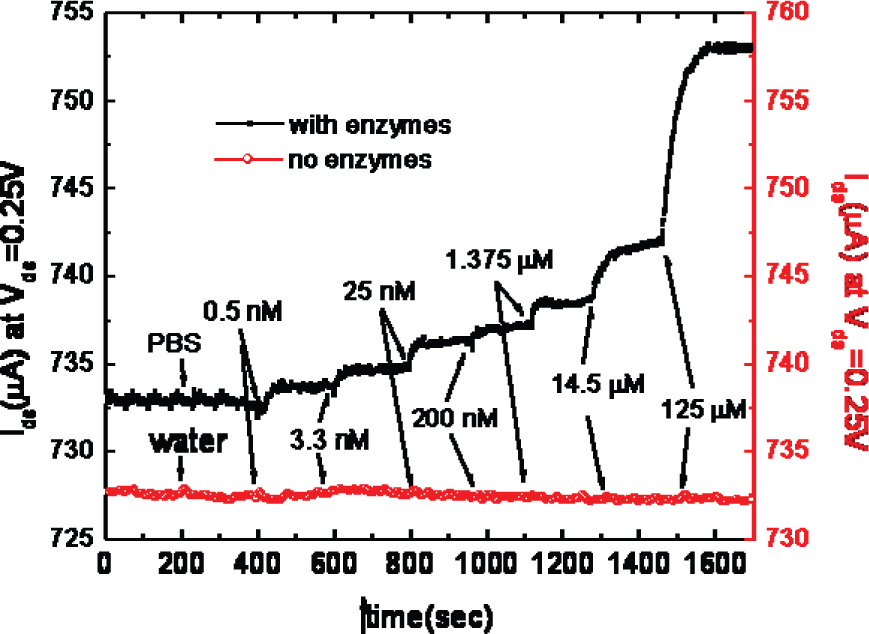
Plot of drain current versus time with successive exposure of glucose from 500 pM to 125 μM in 10 mM phosphate buffer saline with a pH value of 7.4, both with and without the enzyme located on the nanorods.

Change in drain-source current in HEMT glucose sensors, both with and without the localized enzyme.
Although measuring the glucose in the EBC is a noninvasive and convenient method for the diabetic application, the activity of the immobilized GOx is highly dependent on the pH value of the solution. The GOx activity can be reduced to 80% for pH = 5 to 6.
By way of contrast, when the glucose sensor was used in a pH-controlled environment, the drain current stayed fairly constant. In this experiment, 50 μl of PBS solution was introduced on the glucose sensor to establish the baseline of the sensor, as in the previous experiment. Then, glucose at a 10 nM concentration prepared in the PBS solution was introduced to the gate area of the glucose sensor through a micro-injector. There was no glucose in the 50 μl PBS solution and the PBS solution was added at 20 and 30 min. It took time for the glucose solution to diffuse to the gate area of the sensor through the blank PBS, and the drain current gradually increased corresponding to the glucose diffusion process. Since the fresh glucose was continuously provided to the sensor surface and the pH value of the glucose was controlled, once the concentration of the glucose reached equilibrium at the gate of the glucose sensor, the drain current of the glucose remained constant, except in the presence of the glucose solution, which was taken out from time to time using a micro-pipette. Small oscillations of the drain current were observed, which could be eliminated by using a microfluidic device for this experiment.
The human pH value can vary significantly, depending on health. Since we could not control the pH value of the EBC samples, we needed to measure the pH value while determining the glucose concentration in the EBC. With the fast response time and low volume of the EBC required for HEMT-based sensor, a handheld and real-time glucose sensing technology could be realized.
4.2.4 Lactic Acid
Another application for functionalized AlGaN/GaN sensors is the detection and quantification of lactic acid content in breath or blood. This is important in sports training, where the level of exertion and recovery of swimmers and sprinters is necessary to optimize their training practices. It is also important in situations like monitoring of the effectiveness of anaesthetics during medical procedures or for individuals with conditions such as diabetes and chronic renal failure.
A ZnO nanorod array, which was used to immobilize lactate oxidase (LOx), was selectively grown on the gate area using low temperature hydrothermal decomposition (Figure 14, top). The array of one-dimensional ZnO nanorods provided a large effective surface area with a high surface-to-volume ratio and a favourable environment for the immobilization of LOx. The AlGaN/GaN HEMT drain-source current showed a rapid response when various concentrations of lactate acid solutions were introduced to the gate area of the HEMT sensor. The HEMT could detect lactate acid concentrations from 167 nM to 139 μM. Figure 14 (bottom) shows a real-time detection of lactate acid by measuring the HEMT drain current at a constant drain-source bias voltage of 500 mV during the exposure of the HEMT sensor to solutions with different concentrations of lactate acid. The sensor was first exposed to 20 μl of 10 mM PBS and no current change could be detected with the addition of 10 μl of PBS at approximately 40 seconds, showing the specificity and stability of the device. By contrast, a rapid increase in the drain current was observed when the target lactate acid was introduced to the device surface.
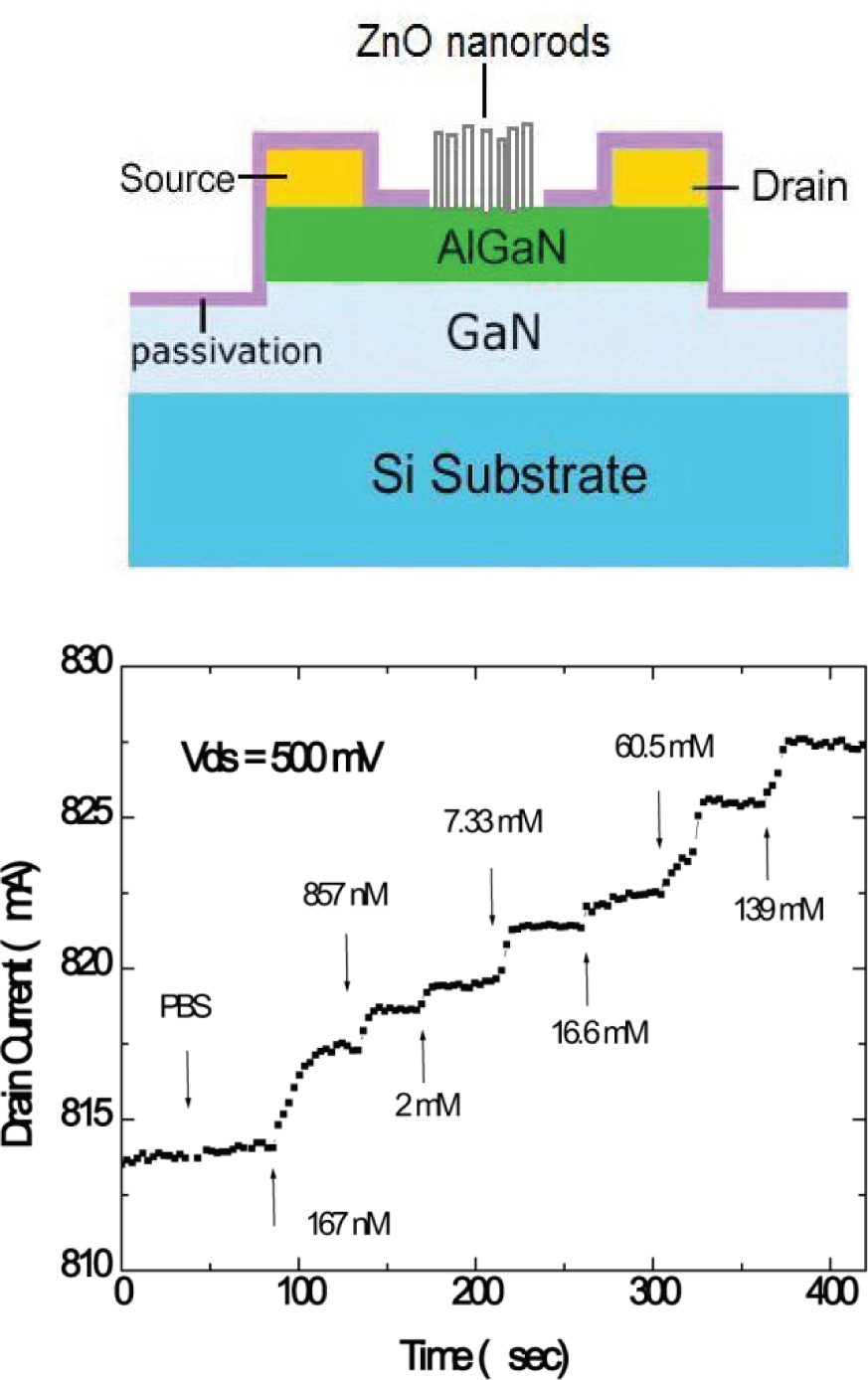
Schematic cross-sectional view of the ZnO nanorod gated HEMT for lactic acid detection (top) and plot of drain current versus time with successive exposures to lactate acid from 167 nM to 139 μM (bottom). (Reprinted with permission from Ref.31 B.H. Chu, B.S. Kang, F. Ren, C.Y. Chang, Y.L. Wang, S.J. Pearton, A.V. Glushakov, D.M. Dennis, J.W. Johnson, P. Rajagopal, J.C. Roberts, E.L. Piner, and K.J. Linthicum, Appl. Phys. Lett. 93, 042114 (2008). Copyright American Institute of Physics).
As compared with the amperometric measurement-based lactate acid sensors, our HEMT sensors do not require a fixed reference electrode in the solution to measure the potential applied between the nanomaterials and the reference electrode. Although the time response of the HEMT sensors is similar to that of electrochemical-based sensors, a significant change of drain current was observed in exposing the HEMT to the lactate acid at a low concentration of 167 nM due to this amplification effect. In addition, the amount of the sample, which is dependent upon the area of the gate dimension, can be minimized for the HEMT sensor due to the fact that no reference electrode is required. Thus, measuring lactate acid in the exhaled breath condensate (EBC) can be achieved as a non-invasive method.
5. Summary and Outlook
Nitride and oxide semiconductor nanostructures are ideal materials for chemical sensing. Material properties, including high chemical and thermal stability coupled with a high surface to volume ratio, give these nanostructured sensors high sensitivity with detection capabilities down to the low ppm levels for gases such as hydrogen. While hydrogen sensing devices have been demonstrated on single ZnO nanowires, there are advantages in the development of wide bandgap sensors involving contacting multiple nanowire sheets. Although the power requirement for using multiple nanowires is higher than that for single nanowire devices, the simplicity of fabrication, including minimal processing steps for multiple nanowire sensors, is highly favourable for the future mass production of these sensors.
The selective sensing of hydrogen in nitrogen ambients has been shown using nanostructured ZnO, GaN and InN down to 50 ppm at room temperature. Sensors were functionalized using Pt or Pd in order to facilitate the dissociation of molecular hydrogen and improve sensing efficiency. All of the sensors displayed excellent response characteristics and decent recovery upon exposure to air or pure oxygen.
There is also great promise for using nanowires in conjunction with HEMT sensors to enhance the detection sensitivity for glucose and lactic acid. Once again, the high surface area of nanowires provides an ideal approach for enzymatic detection of biochemically important substances [15–30].
Footnotes
6. Acknowledgments
The work at UF was partially supported by NSF (J.M. Zavada).