
Abstract
The objective of this research is to study the influence of film thickness on the optical and electrical properties of prepared NiO thin films. Nickel oxide thin films have been prepared on the glass substrates by a spin coating technique using nickel nitrate hexahydrate (Ni(NO3)2.6H2O) as a source of materials. The coating process was repeated 11, 13, 15, and 17 layer times to obtain a good NiO thin film. The optical and electrical characterizations were observed to be dependent on each film thickness. The smaller layers have a high optical transmission (over 88%) in the visible range. The bandgap energy was found to be in the range of 3.94–4.06 eV depending on the film thickness. The lowest value of Urbach energy was 0.182 eV. The electrical measurements are investigated by the four-point method; the results show that good electrical conductivity was found for the sample with a thickness around 171 nm.

Introduction
Recently, metallic oxide semiconductors have been of interest for the development of the ultra-high-frequency components used in gas sensors, photocatalysis, optoelectronics, lithium ion micro-batteries, and enamels and as cathode materials for alkaline batteries. Among these, nickel oxide (NiO) is a semitransparent p-type semiconducting material with a large direct gap (3.6–4.0 eV).1,2 NiO exhibits face-centered cubic structure.3,4 In bulk form, NiO is antiferromagnetic in nature. However, at room temperature, NiO thin films exhibit ferromagnetic behavior.5,6 NiO thin film has high thermal and chemical stability with excellent electrical, optical, magnetic, electrochromic, and electrochemical properties.7,8 Hence, it has a wide range of applications, such as in gas sensors, photocatalysis, memory devices, spintronic devices, dye sensitizers, electrochromic coatings, UV photodetectors, solar cells, light-weight structural components for aerospace, ceramic structures, and counter electrodes and in the anode layers of solid, counter electrode oxide fuel cells.9–11
NiO thin films can be obtained by several deposition methods, including electrochemical deposition, pulsed laser deposition, magnetron sputtering, molecular beam epitaxy, reactive evaporation, sol–gel processes, chemical vapor deposition, and spray pyrolysis.12,13 Among the above-mentioned techniques, sol–gel spin coating is a simple and effective method for coating thin films. It requires less equipment, low cost, and is faster when compared to other coating techniques. In this study, NiO thin films are synthesized using sol–gel spin coating method. NiO has been intensively studied as a promising material due to its high stability similar to ZnO.14,15
The previous research works mainly focused on the structural, optical, and electrical properties of NiO thin film as a function of different precursors, different substrates, and annealing temperature.12–18 The influences of film thickness on the optical and electrical properties of thin films are very important. However, only few works on the dependence of the properties of NiO films on film thickness have been published.19,20 The main objective of the this work is to study the influences of film thickness on the optical and electrical properties of NiO thin films. NiO films obtained by sol–gel spin coating method were analyzed to understand the role of film thickness on the optical and electrical properties of the NiO films. The thickness of the films was varied between 131 and 237 nm. Therefore, this study is important for future applications of NiO thin films on electronic devices, such as solar cells, sensors, and photodetectors, among others.
Results and discussion
Transmittance spectra
The optical transmittance spectra of thin NiO films with several film thicknesses are presented in Figure 1. The optical transmittance is a function of the length of the wavelength and was studied between 300 and 1000 nm. As can be seen, thin films are highly transparent (>80%) in the visible range. However, at lower wavelengths (<400 nm), they are only weakly transparent. It has been observed that for large thicknesses, the transmittance is less than 60%; this is due to the nature of the material.
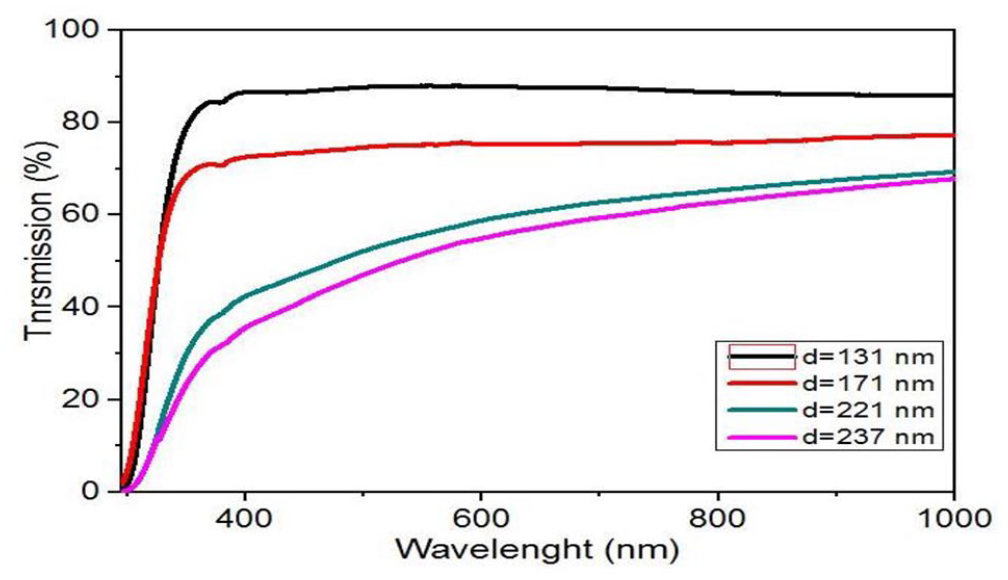
Optical transmittance spectra of NiO thin films.
The minimum reflectance in NiO thin films was obtained at lower film thickness (Figure 2). As can be seen, the film is transparent in the visible range.

Reflectance spectra of NiO thin films.
Optical gap
The optical bandgap Eg was determined from the optical transmission spectra of the thin NiO films and was obtained by extrapolating the linear portion of the plot (αhυ)2 versus (hυ) to α = 0. The method for designing the extrapolation was according to the following equation18,19

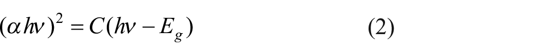
where A is the absorbance, C is a constant, hν is the photon energy, and Eg is the bandgap energy of the semiconductor. As is shown in Figure 3, optical bandgap Eg is deduced using a typical variation of (αhυ)2 as a function of photon energy (hν). Table 1 presents the obtained values of Eg.
The variation of (αhυ)2 as a function of hν for each film thickness.
The bandgap energy Eg and the Urbach energy Eu.

The disorder (Urbach energy)
Figure.4 shows a typical variation of (Ln α) versus photon energy (hν) of NiO thin film for deduction of the Urbach energy, which is related to the disorder in the film network, and expressed as follows 20

The variation of Ln α as a function of hν for each film’s thickness.

where α0 is a constant and Eu is the Urbach energy. The Urbach energy Eu is given in Table 1.
Figure 5 shows the variation of the bandgap energy Eg and the Urbach energy Eu as a function of a film’s thickness. The optical gap and disorder vary inversely; it is observed that the bandgap energy and Urbach energy of NiO thin films increased with increasing film thickness up to 172 nm, and then the optical gap energy decreased at 221 nm. This result can be explained by the decrease in optical transmittance of the films (Figure 2).

Changes of the bandgap energy Eg and the Urbach energy Eu as a function of film’s thickness.
Refractive index
The refractive index (n) is an important parameter for the characterization of optical materials and provides valuable information for more efficient optical materials. In this work, the refractive index (n) can be calculated using the following formula 13

where n is the refractive index, R is the reflectance, and K is the extinction coefficient of NiO thin films.
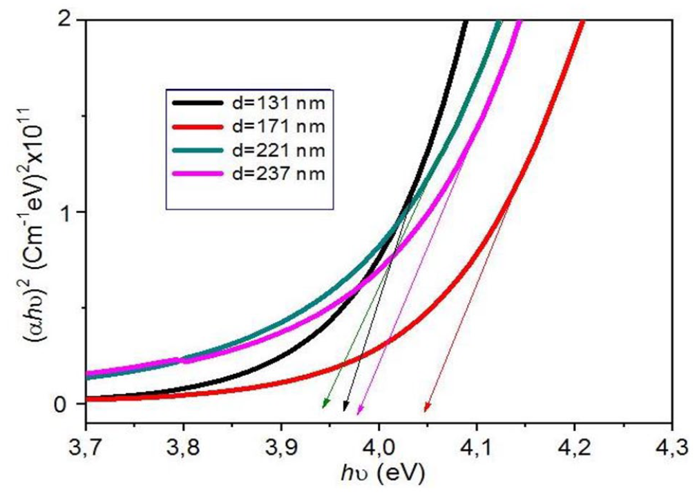
The variation in refractive index as a function of wavelength for the spectral range 400–1100 nm for NiO thin films is shown in Figure 6. It can be seen that the value of the refractive index decreases at longer wavelengths. The refractive index increases with increasing film thickness up to 237 nm and is in the range of 1.7–2.6.
The relation between the refractive index and the length of the wavelength for nickel oxide thin films at several film thicknesses.
Extinction coefficient
The extinction coefficient (K) was calculated using the following relationship

where λ is the wavelength and α is the absorption coefficient that can be estimated from the absorbance using the following formula 21

where d is the thickness of the NiO thin films. Figure 7 shows the relationship between the extinction coefficient (K) and wavelength λ.
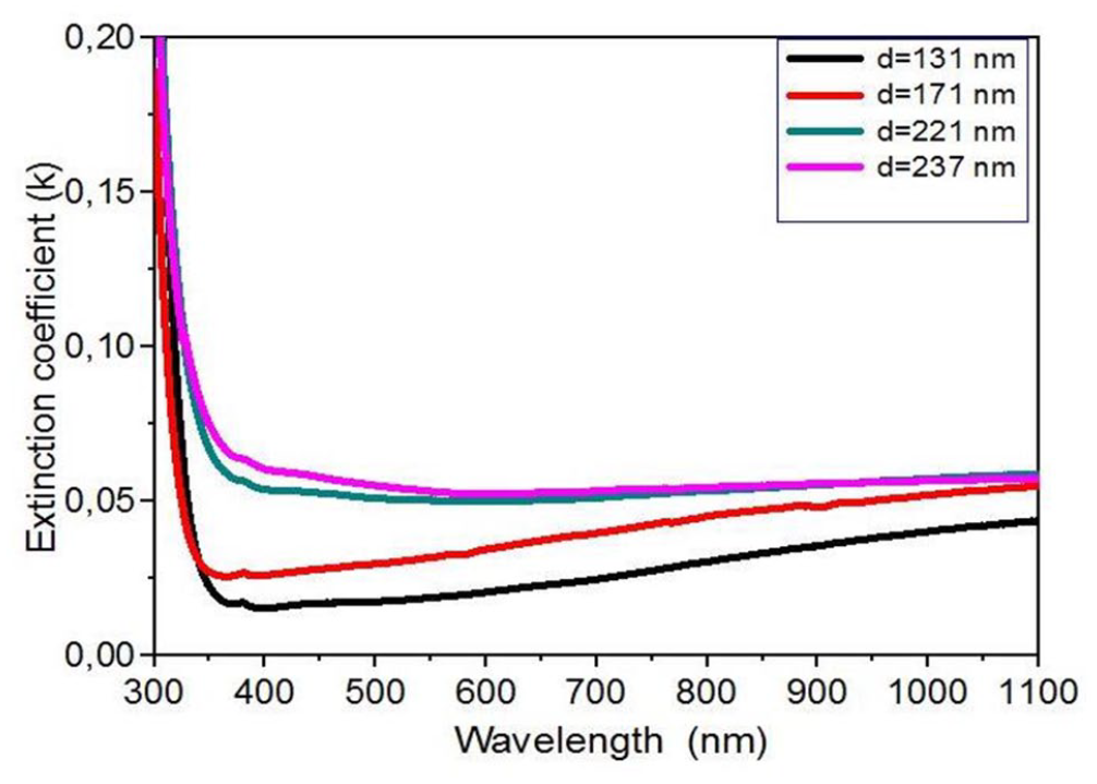
The relation between the extinction coefficient and the length of the wavelength for nickel oxide thin films with several film thicknesses.
Electrical properties
The four-point method was used to determine the sheet resistance (Rsh). A variation in the current (I) was applied between the outer two leads and the potential difference (V) was measured; this model was applied in the linear. This method is well important in electrical property by comparing with others; however, the sheet resistance Rsh was calculated from the following relation 14

where I is the applied current of 5.10−8 A and V is the voltage measured.
Table 2 and Figure 8 give the sheet resistance Rsh of the NiO thin films as a function of films’ thicknesses.
The sheet resistance Rsh and the electrical conductivity σ for different film thicknesses.

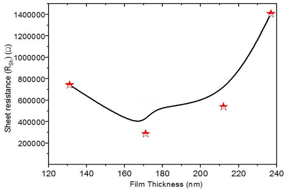
Changes in the sheet resistance of the NiO films with several film thicknesses.
The electrical direct conductivity σ equals the inverse of resistivity according to the following equation 22


The conductivity as a function of NiO film thickness is given in Table 2. It is observed that the conductivity increases at 171 nm and then decreases with increasing film thickness up to 237 nm. This observation of an increase in conductivity has been explained with the tail width of the localized states within the optical bandgap (Urbach energy). A decrease in the resistance can be expected with an increase in the film thickness. As can be seen, films with a thickness of 237 nm exhibit good electrical properties.
Figure of merit
A figure of merit (FOM) is a tool for a fine comparison of transparent conductive oxide (TCO) films in optoelectronic development. For more information about prepared NiO thin films, it can be compared by the use of Haacke’s FOM. 23 It is defined as the ratio of photocurrent density over TCO sheet resistance, and the FOM could be calculated using Haacke’s formula 23

where T and Rsh are transmittances and sheet resistance, respectively. The variation of the calculated FOM values of the prepared NiO thin films at several film thicknesses is shown in Figure 9. We noted an enhancement of the values of the FOM in the visible region. It is clear from the Figure 9 that the high FOM is observed at higher film thickness. In this work, the optimum of the medium FOM was achieved at 131 nm.
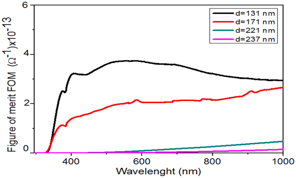
Figure of merit of NiO thin films with several film thicknesses.
Conclusion
NiO thin films with different thicknesses have been deposited on ordinary glass substrates using a spin coating method. The number of coatings was varied to produce different thicknesses of the thin films. The coating process was repeated 13–17 times to obtain the thin film. The optical and electrical properties were found to be dependent on the film thickness. Thinner films showed high transmittance (over 88%) in the visible wavelength region. The optical bandgap was found to be in the range of 3.94–4.06 eV depending on the film thickness. The minimum value of the Urbach energy was 0.182 eV for samples that were 131 nm thick. Good conductivity was found for films with a thickness of 171 nm, due to an increase in carrier mobility.
Experimental study
Spin coating method
The spin coating method of depositing NiO thin films gives layers of high quality and good properties. In this work, we deposited the thin films by a spin coating method which is the most suitable method to fabricate nanocrystalline thin films with high purities. In this method, the surfactants, solvents, reaction time, and temperature are the main factors in obtaining a suitable solution with remarkable quality. The synthesis consists of four stages expressed as follows:
The preparation of precursor solutions.
The formation of the intermediate NiO sol.
The conversion from NiO in solution to gelatin NiO.
Calcination.
Preparation of the solution
Mass of 4.652 g from nickel nitrate hexahydrate (Ni(NO3)2,6H2O) was dissolved in 20 mL of water to give 0.8 M of NiO precursor solution. A few drops of hydrochloride acid were added as a stabilizer to the solution. The mixture was stirred and heated at 40 °C to give, after 2 days, a highly transparent solution.
Depositing of thin films
NiO thin films were synthesized by a spin coating process. The first sample was prepared by dropping the coating solution onto a glass substrate (2.5 × 1.5 × 0.1 cm3), which was rotated with 2500 r/min for 30 s using a spin coater. The coating process was repeated 11, 13, 15, and 17 times to obtain the thin films. A preheat treatment temperature of 200 °C is required to initiate the formation and crystallization of the NiO films. After the deposition, the thin films that were obtained were annealed at 600 °C in the air for 2 h.
Crystallization of the layers
Finally, the samples were placed in a furnace and crystallized at a temperature of 600 °C for 2 h to obtain homogeneous surfaces of NiO which improve the electrical conductivity.
Characterization of the films
The optical and electrical properties of NiO thin films were evaluated using several characterization techniques including the following.
The transmittance spectra of samples were measured using a UV–visible spectrophotometer (25-LAMBDA) at room temperature in the wavelength range of 300–1000 nm.
The electrical conductivity was measured by injection of current–voltage using a four-point method. All characterizations have been made at stable conditions.
Footnotes
Declaration of conflicting interests
The author(s) declared no potential conflicts of interest with respect to the research, authorship, and/or publication of this paper.
Funding
The author(s) received no financial support for the research, authorship, and/or publication of this paper.