
Abstract
A three-phase three-level transformerless T-type grid-connected inverter system with three-level boost maximum power point tracking converter is introduced in this article for high-voltage high-power applications. First, the mathematical model of grid-connected photovoltaic inverter system is built. Second, a multiloop interleaved control scheme is proposed for three-level boost maximum power point tracking converter to reduce the ripple of the inductor current and balance the capacitor voltage of DC bus. A predictive current control method and a power feedforward strategy are also proposed for the T-type three-level inverter part to reduce the harmonic content of grid-connected current and to improve the dynamic response of the system, respectively. In order to solve complex algebraic computation of traditional space vector pulse width modulation or multi-carrier pulse width modulation method, a single-carrier pulse width modulation method is presented for T-type three-level inverter. Finally, all control strategies and modulation method are implemented on a single-chip digital signal processor. A high conversion efficiency, low cost, and low harmonic current could be obtained on a 23-kW experimental prototype.
Keywords
Introduction
With the development of distributed energy system, grid-connected inverter is the core equipment of solar energy, wind energy, other renewable energy systems, and grid interface.1–5 The topology and the control methods have attracted wide attention from domestic and foreign scholars. Three-level topology is widely used in the high-voltage high-power applications, because of the advantages of the small output harmonic content, the low switch voltage stress, the small voltage change rate (du/dt), and high efficiency of inverter.6–10 Compared with the traditional neutral-point-clamped (NPC) three-level topology, T-type three-level topology has the following advantages: a small number of diodes, high efficiency, and low power loss.9,10
The modulation and control strategies have been the research focus in the three-phase inverter system.11–14 The digital predictive current control, repetitive control, and instantaneous power control strategy are proposed in Lidozzi et al., 12 Rivera et al., 13 and Akagi et al. 14 for three-phase inverter system to achieve low harmonic current and high dynamic performance, respectively. In order to obtain the low cost, high efficiency, and low distorted grid-connected current, a T-type three-level inverter topology with three-level boost maximum power point tracking (MPPT) controller and related control strategies are proposed for high-power photovoltaic (PV) applications. In this article, a multiloop interleaved control scheme is proposed for three-level boost MPPT converter to reduce the ripple of the inductor current and balance the capacitor voltage of DC bus. For the purpose of reducing the delay time caused by digital control, a novel predictive current control strategy is used to improve the quality of grid-connected current waveform. A power feedforward strategy is also introduced to improve the dynamic response of the system. As traditional space vector pulse width modulation (SVPWM) 15 or multi-carrier pulse width modulation (MCPWM)16,17 has the drawback of complex algebraic computation, a single-carrier pulse width modulation (PWM) method which is suitable for digital implementation is presented for T-type three-level inverter. Finally, the proposed control and modulation strategy are verified on a 23-kW prototype. Simulation and experimental results show that the whole system has excellent static and dynamic performance, high conversion efficiency, and low total harmonic distortion (THD) current.
The mathematical model of three-phase grid-connected PV system
The main circuit of three-phase T-type three-level grid-connected PV system is shown in Figure 1. The three-level boost DC/DC part performs MPPT control and also gives step-up function of the PV voltage. The T-type three-level three-phase DC/AC part regulates the DC bus voltage and generates the AC power.

Main circuit structure of the grid-connected PV system.
Three-level boost DC/DC converter part
As multilevel DC/DC converter has several advantages in high voltage applications, such as smaller inductor, lower switching voltage stress, and lower switching losses, and the PV cells also have a wide range of output voltage, three-level boost DC/DC topology is suitable for high-voltage high-power MPPT applications of PV system.18–22UPV is the output voltage of the PV cells, C1 and C2 are divided voltage capacitors, QT1 and QT2 are power switches, D1 and D2 are diodes, and L is the boost inductor.
There are four possible switching states in the operation of the three-level boost converter as shown in Figure 2. To simplify the analysis, the three-level boost converter works in continuous conduction mode (CCM), the capacitors C1 and C2 are large enough, and UC1 = UC2 = 0.5 UDC.

Operating modes of the three-level boost converter: (a) mode 1, (b) mode 2, (c) mode 3, and (d) mode 4.
Mode 1: As shown in Figure 2(a), QT1 and QT2 turn on, D1 and D2 reverse turn off, and the inductor current rises linearly. The output bus voltage (UDC=UC1+UC2) and inductor current IL can be expressed as
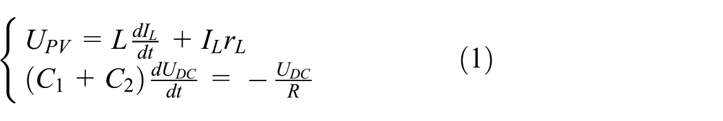
where R is the equivalent resistance of the DC/AC inverter part and rL is the equivalent resistance of the boost inductor.
Mode 2: As shown in Figure 2(b), QT2 and D1 turn on and QT1 and D2 turn off. The output bus voltage and inductor current IL can be expressed as

Similarly, it is easy to conduct the other two modes. According to the four working modes and equations (1) and (2), the state-space average method of the three-level boost converter can be expressed as

The AC small signal disturbance is added in equation (3), where the small signal disturbance is
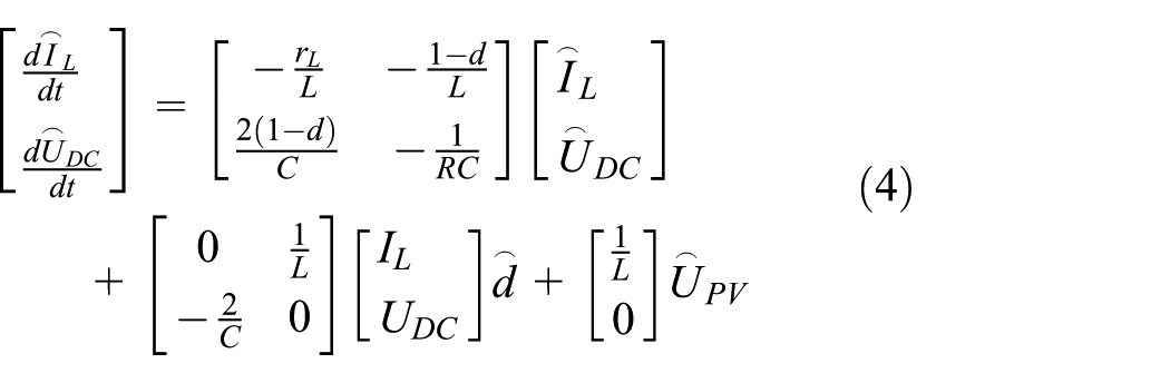
The dynamic mathematical model of the three-level boost converter from control to output can be obtained by equation (4)

It can be concluded that the mathematical model of d > 0.5 or d < 0.5 is identical based on mathematical model analysis.
Three-phase T-type DC/AC grid-connected inverter part
The T-type grid-connected inverter is shown in Figure 1. Lj is the AC side filter inductor, j = a, b, c; UC1 and UC2 are the positive and negative bus voltage; Qj1-j4 is power switching device; ej is the grid voltage; and Sj is defined as the output state of each bridge leg.
Table 1 shows a phase bridge leg switch variable Sa corresponding to the switching states of each power switching device. The driver signals of Qa1, Qa3, and Qa2, Qa4 are complementary. The b phase and c phase are similar to a phase. UDC/2 represents half of the DC bus voltage. Twenty-seven kinds of switch states can be achieved from three-phase T-type three-level inverter.
Switching states of a phase.

It is assumed that the AC voltage is a balanced three-phase power supply as shown in Figure 1; the mathematical model of the grid-connected inverter based on the three-phase stationary a, b, and c reference frames can be obtained according to the Kirchhoff current definition
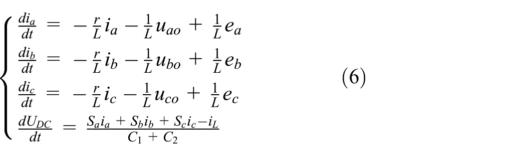
where ia, ib, and ic are the gird-connected current for each phase; r is the inductor equivalent resistance of the T-type three-level AC side; and uao, ubo, and uco are the voltage between the neutral point of the bridge arm and the neutral point of the grid. Sa, Sb, and Sc are switch functions.
The three-phase model based on stationary frame can be transformed into rotating d-q frame, and the mathematical model can be written as

where, ed, eq and id, iq denote the grid voltage and the grid-connected current in the rotating d-q reference frame, and Sd and Sq are switch functions.
Research on control strategy of PV system
Multiloop interleaved control for three-level boost
The maximum power tracking reference voltage Vr can be searched by sampling the voltage and current of PV panel and using P&O method to search the MPPT point. By analyzing the working principle of the first-stage converter structure, the working state of power switch can be obtained as shown in Figure 3, where d1 and d2 are the duty cycle of the power switch QT1 and QT2, respectively, IL is the value of inductor current, Ts is the switching period, and θ is the phase difference of drive signal, θ = π.
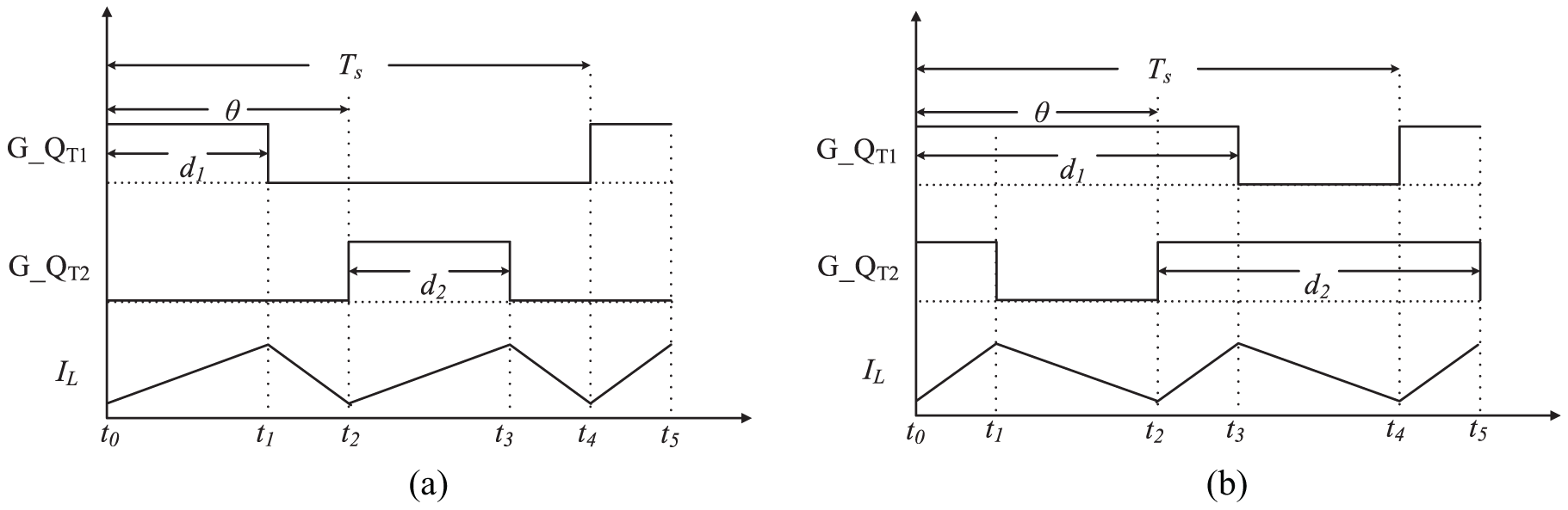
Working state of power switch: (a) d < 0.5 and (b) d > 0.5.
As we know, the total DC bus voltage UDC is regulated by the inverter, 18 but we must ensure the equal balancing of two capacitor voltages UC1 and UC2 to make sure that each power switch needs to withstand only one half of DC bus voltage stress. Since the capacitors C1 and C2 are alternatively charged, their voltages UC1 and UC2 are theoretically balanced. In fact, as the parameters of the components are not completely the same, it makes the actual duty cycles of two power switches different. Therefore, it can be concluded that the neutral point voltage is unstable. In order to maintain the neutral point voltage stable, an additional voltage balance control-loop is required as shown in Figure 4 to balance both capacitor voltages UC1 and UC2.
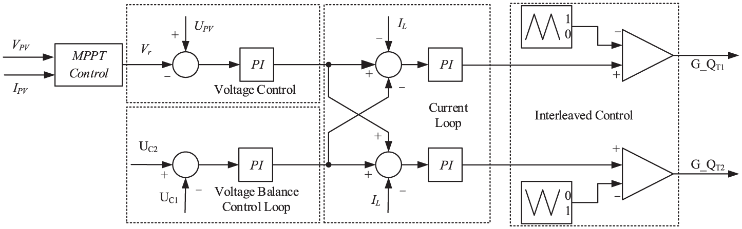
Multiloop interleaved control scheme for step-up.
Under the working mode 2 (capacitor C1 stores energy and capacitor C2 releases energy), the voltage difference of the two capacitors is related to the conduction time of QT2, which is related to the duty cycle of d2. Under the working mode 4 (capacitor C1 releases energy and capacitor C2 stores energy), the situation is the opposite, which is related to the duty cycle of d1. Therefore, the capacitor voltages UC1 and UC2 could be balanced by sampling the value of voltages UC1 and UC2 and adjusting the duty cycle of d1 and d2 in one switching period. For example, when the capacitor voltage UC1 > UC2, we should extend the conduction time of QT1 and shorten the conduction time of QT2 (d1 rise and d2 decline). When the capacitor voltage UC1 < UC2, the situation is the opposite (d2 rise and d1 decline).
In order to yield smaller inductor current ripple and lower voltage stress of the switches, a strategy combines the multiloop control and the interleaved PWM. Both the voltage and current controller are proportional–integral (PI) type controllers. The multiloop interleaved control scheme for the three-level DC/DC part is shown in Figure 4.
Predictive current control for unity grid-connected current
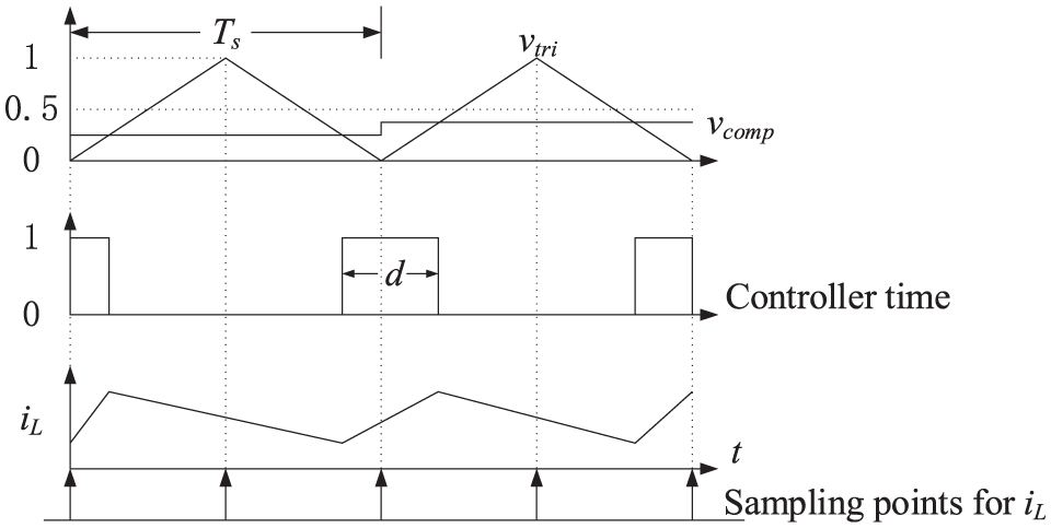
The conventional control methods have the drawbacks of sampling delay and low control precision. When the prototype is implemented by a digital signal processor (DSP), it is found that the delay of the filter in the hardware sampling circuit and the process of calculation will affect the quality of grid-connected current. In order to overcome these problems, the sampling value must be predicted. The predictive current control is based on the present current sampling value to predict the current of the next moment as the feedback current value, which can eliminate the delay caused by sampling and calculation.
The proposed sampling and hold strategy is shown in Figure 5. Two samples were completed during the timer cycle interrupt and underflow interrupt. According to the hardware circuit and the proposed current sampling method, the best predicted time is Ts/2, where Ts is the switching period. The deduction principle of prediction formula is shown in Figure 6.
Proposed sampling and hold strategy.

Deduction principle of prediction formula.
In Figure 6, xk is the sampling time, ik is the corresponding current sampling value at time xk, i4 is the present current sampling value, im is the forecast current value, xk minus xk-1 is equal to the switching period Ts, k = 1, 2, 3, 4, and xm minus x4 is equal to Ts/2.
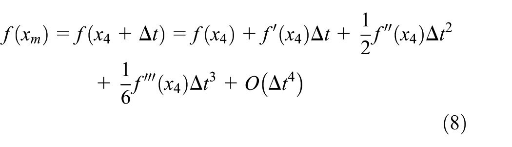
The value of predicted current can be obtained by Taylor expansion
The sampling time interval is very short, so that the sampling period is very small in the system. The formula can be easily obtained by approximately replacing the linear formula when calculating the derivative formula

Equation (10) can be obtained by substituting Δt = T/2 into equation (8), as follows

Predictive control has the advantage of simplicity, and it is easy to be implemented digitally by programming. By using the prediction control strategy, the system has good performance of static and dynamic response.
Power feedforward control for fast response of DC voltage regulation
As we know, when the light intensity changes, the maximum output power of PV panel changes accordingly. If the dynamic response of inverter system is not fast enough, the DC bus voltage will fluctuate significantly, and it will lead to the occurrence of overvoltage protection or damage the power devices. A power feedforward strategy is proposed to restrain the DC bus voltage fluctuation caused by the PV output power disturbances in this article.
The conventional control strategy of double close-loop is widely used in grid-connected applications, and the DC bus voltage is regulated by the voltage-loop and the grid-connected current is regulated by the current-loop, but the whole system has slow dynamic performance. In this article, the direct connection between PV input power and output grid-connected current can be established by the power feedforward method, as shown in Figure 7. When the PV input power changes, the power information of PV side can be directly transferred to the grid-connected current-loop without the regulation of voltage-loop. In order to obtain unity power factor of AC power grid side, the value of reactive current reference

The double closed-loop control block diagram with power feedforward control strategy.
According to the theory of instantaneous power, 14 the instantaneous active and reactive power of the grid-connected inverter can be expressed in the synchronous d-q reference frame as

Assuming that the three-phase grid voltage is symmetrical, eq is zero, and the amplitude of the supply voltage ed is constant, the active and reactive power of the PV system can be indirectly controlled by the id and iq.
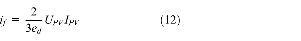
If the power loss in the process of power conversion can be ignored, it is considered that the PV input power is equal to the grid-connected power. The feedforward current can be expressed as
Single-carrier modulation strategy
Modulation technology is one of the most important issues for three-phase PV system. SVPWM and MCPWM are two typical modulation strategies, but these methods require complex algebraic computation or implementation. In order to overcome the shortcoming, a single-carrier modulation method is proposed in this article, which has the advantage of simplicity and a small amount of algebraic computation.
According to Table 1, it can be observed that Qa1, Qa3 and Qa2, Qa4 are complementary in three-phase T-type three-level inverter. In order to improve the conversion efficiency, according to the polarity of modulation wave voltage, part of the switches operate in the power frequency state and part of switches operate in high frequency state as shown in Figure 8.

Switch working states of the three-level inverter.
When the modulation wave um > 0, Qa1 and Qa3 work in high frequency state, where Qa2 has been turning on and Qa4 has been turning off. If Qa1 turns on and Qa3 turns off, then the output voltage is UDC/2. Otherwise, the output voltage is zero. When the modulation wave um < 0, Qa2 and Qa4 work in high frequency state, where Qa3 has been turning on and Qa1 has been turning off. If Qa4 turns on and Qa2 turns off, then the output voltage is –UDC/2. Otherwise, the output voltage is zero.
According to the working principle of Figure 8, the working states of the power switches can be obtained from the modulation wave compared with single-carrier in this article. The three-phase T-type three-level grid-connected inverter based on single-carrier PWM method is presented as shown in Figure 9. The neutral point voltage balance can be realized by the offset of modulation wave. It also could be implemented in a DSP. In order to improve the voltage utilization of the DC side, the third-order zero sequence components are injected into the modulation wave.

Proposed single-carrier modulation method.
The analysis of stability and switching loss evaluation
The stability analysis of PV system
The PV inverter system discussed in this article has been investigated. Thus, it is necessary to maintain the designed system with good performance and have high reliability. Since the PV inverter system adopts two-stage structure, it is necessary to analyze the stability of the first-stage and second-stage structures to ensure the good performance of the whole PV system, respectively.
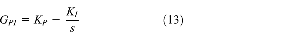
For the first-stage structure, the stability of the three-level boost converter can be obtained by analyzing the bode diagram. In order to make the three-level boost converter have satisfactory dynamic response characteristics, PI controller can be added to improve the dynamic performance of the system. Equation (13) is an expression of the PI controller, where KP = 4 and KI = 80. Therefore, equation (5) has a frequency response characteristic as shown in Figure 10. By adding PI controller, the crossover frequency and phase margin are 557 Hz and 81.8°, respectively.

Bode plot of three-level DC/DC converter part.
In addition, the stability of the three-level grid-connected inverter can be obtained by analyzing the bode diagram for the second-stage structure. According to equation (7), it can be found that the inner current-loop has symmetry. Thus, the stability of the current regulator is discussed below with the d-axis component. Figure 11 shows the simplified structure of decoupling inner current-loop, where GPC is the lead block of the predictive current control part,

The simplified structure of decoupling inner current-loop (without disturbance).
In general, when

where τi is time constant, τi = L/r = KiP/KiI.
Figure 12 shows the bode plot of the current-loop of the three-level inverter part, where KiP = 2 and KiI = 220. The magnitude crossover frequency of the current regulator occurs at 244 Hz. Simultaneously, the phase plot shows a phase margin of 64.7° at this frequency. Therefore, it is obvious that the system is stable.

Bode plot of the current-loop of the three-level inverter part.
Switching loss evaluation
The switching losses are divided into switching loss and conduction loss. However, the different power modules have different loss characteristics. Therefore, it is necessary to analyze the loss of power switch.
For the first-stage structure, the power module of FZ06NBA050SA-P915L33 was used in the experiment. The insulated-gate bipolar transistor (IGBT) switching loss (PB-sl-IGBT) and the IGBT conduction loss (PB-cl-IGBT) are calculated as follows

where Vce is collector–emitter voltage of the IGBT, Ic is the collector current of the IGBT, DIGBT is the duty cycle of the IGBT, Eon and Eoff are the IGBT turn on and turn off energy losses, and fs is the switching frequency.
The switching loss (PB-sl-diode) and the conduction loss (PB-cl-diode) of the diode can be calculated as follows

where Vf is the diode voltage drop, If is the diode forward current, Ddiode is the duty cycle of the diode, and Erec is the reverse recovery energy loss.
In addition, for the second-stage structure, the power module of FZ12NMA080SH01-M260F was used in the experiment. For the two IGBTs on the bridge arm, the switching loss (PI-sl-1/4) and the conduction loss (PI-cl-1/4) can be calculated as follows
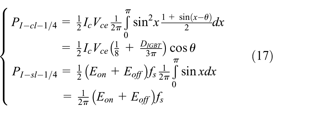
where cos θ is the output power factor of PWM.
In this case, the diode in the module has no freewheeling state. So the diode losses in this form can be represented by

For the two IGBTs at the midpoint, the switching loss (PI-sl-2/3) and the conduction loss (PI-cl-2/3) are calculated as

In this case, the diode in the module has a freewheeling state and the freewheeling time is half of a power frequency cycle. So the diode losses in this form can be represented by

To analyze the switching losses of the whole system, it is assumed that the room temperature is 25°C, the power factor is 1, and the modulation ratio is 0.8. Figure 13 shows the efficiency analysis result. Figure 13(a) shows the switching losses of a single power switch in the module and Figure 13(b) shows the switching losses of the whole module.

Switching loss analysis result: (a) the switching losses of a single power switch in the module and (b) the switching losses of the whole module.
Simulation and experimental results
In order to verify the validity and feasibility of the proposed control and single-carrier modulation strategies, the simulation and experimental verification are carried out based on a 23-kW three-phase T-type three-level grid-connected prototype as shown in Figure 14. The parameters of the whole system are summarized in Table 2.
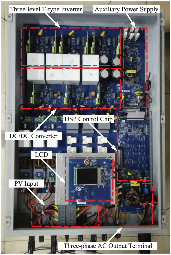
The whole of two-stage prototype.
System parameters of the prototype.

PV: photovoltaic; MPPT: maximum power point tracking.
All the control algorithms were implemented by using a single-chip TMS320F28335 (DSP) as a digital controller as shown in Figure 15. The grid voltage, input current, the DC bus capacitor voltage, PV voltage, and current signals were measured by using the 12-bit AD converter in the DSP.

Control diagram of PV system.
Figure 16 shows the PV output power–voltage curve; it can be seen that the output voltage is close to 550 V when the PV cells operated at maximum power point. In addition, the dynamic waveforms of voltage VPV and current IPV displayed in Figure 17 show that the proposed DC/DC controller has a high performance when the whole system achieves the maximum power point.

Experimental results with MPPT control.

Waveform of PV output voltage and output current.
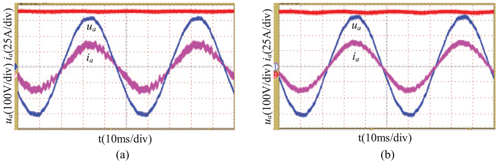
Figure 18 shows the simulation and experimental waveforms of input voltage and input current at the rated output power of 23,000 W. The input current is close to a sinusoidal waveform, and it is in phase with the input voltage. The power factor and the value of total harmonic distorted current are shown in Figure 19. A high power factor of 0.9993 could be achieved, and the measured THD of the grid current is 1.19%, as shown in Figure 20.

Waveform of grid voltage and output current: (a) simulation waveform of a phase grid voltage and three-phase output current and (b) experimental waveform of a phase grid voltage and three-phase output current.

Power factor and value of total harmonic current.

Results of total harmonic current.
Figure 21 shows the experimental waveform of two power switches’ driver signals: DC bus voltage and inductor current in three-level DC/DC converter. It can be seen that the ripple of the inductor current is small by the proposed interleaved scheme.

Experimental waveform of power switches drive signals, DC bus voltage and inductor current: (a) d < 0.5 and (b) d > 0.5.
The two capacitor voltages of DC bus are shown in Figure 22, and the voltage of two capacitors keep balance with the proposed voltage balance control-loop.

Experimental waveform of two capacitor voltage in DC bus voltage and grid current.
The voltage waveforms of a phase driver are shown in Figure 23. It can be seen that part of the switches operate in the power frequency state, and part of switches operate in high frequency state, so low switch loss could be achieved.

The voltage waveforms of a phase driver.
Figure 24 shows the output current and a phase grid voltage waveform of T-type three-level inverter with the traditional current feedback control and the predictive current control under the 17 kW load condition. It can be seen that low THD of grid-connected output current could be achieved with the predictive current control strategy.
Output current and a phase grid voltage waveform of T-type three-level inverter with the traditional control and the predictive current control: (a) without predictive current control and (b) with predictive current control.
Figure 25 shows the dynamic performance of the DC bus voltage and grid-connected current with a sudden power change in the PV side. It can be seen that if the transient process is greatly reduced with the power feedforward control strategy, the high performance of DC bus voltage regulation could be achieved.

Dynamic performance of DC bus voltage: (a) without power feedforward control and (b) with power feedforward control.
Figure 26 shows the conversion comparison efficiency between the proposed three-level boost three-phase T-type inverter and the conventional two-stage inverter which comprises two paralleled two-level boost converter and NPC-type inverter 23 under all load conditions. It can be clearly seen that the proposed three-level boost T-type inverter has obvious advantages over the two-level boost and NPC inverter. Due to the use of a much smaller inductor and lower voltage devices, a high efficiency is reached over a wide load range, and the maximum conversion efficiency is achieved 98.18% in AC voltage 230 V/50 Hz.
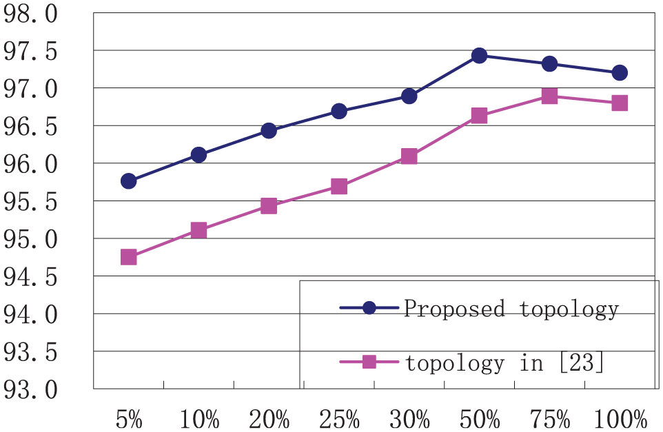
Conversion comparison efficiency.
Conclusion
A three-phase T-type three-level grid-connected inverter for high-voltage high-power is presented in this article. To improve the conversion efficiency, reduce the THD of grid-connected current, and enhance the dynamic response performance of the PV system, a multiloop interleaved control method for DC/DC part, a predictive current, and a power feedforward control strategy for inverter part are proposed, respectively, and a single-carrier PWM method is also proposed to simplify the calculation. Finally, a high efficiency and low cost could be achieved by using small inductor and low voltage devices, and the effectiveness and validity of the proposed method is verified by the experimental results.
Footnotes
Handling Editor: James Baldwin
Declaration of conflicting interests
The author(s) declared no potential conflicts of interest with respect to the research, authorship, and/or publication of this article.
Funding
The author(s) disclosed receipt of the following financial support for the research, authorship, and/or publication of this article: This work was financially supported by Distinguished Young Teacher Project of Education Department of Guangdong Province (YQ2015156), the Industry-University-Research Collaboration of Dongguan Dongcheng District (2016), China and Dongguan Greenway Technology Co., Ltd in China.