
Abstract
The mechanical properties of a material can be positively or negatively affected by its applied or residual stress. In this article, a series of molecular dynamic simulations were adopted to investigate the nanoindentation response of monocrystalline copper under tensile pre-deformation. Nanoindentation simulation under stress-free condition was compared with those under pre-tension strain values of 1.2%, 2.4% and 3.6%. Load–displacement curves with hardness value and recovery rates of total work for nanoindentation based on various tensile pre-deformations were obtained and discussed. It indicated that tensile pre-deformations resulted in a higher potential energy in substrate and a lower external energy will be introduced to realize the same elastic or plastic deformation during indentation. Moreover, the evolution of interior defects during indentation was also observed and analysed. The results showed that tensile pre-strain can influence dislocation nucleation behaviour of material during indentation. This article proposed a special molecular dynamic simulation method to characterize the mechanical properties of the material under tensile pre-deformations via nanoindentation, which gives an effective approach to characterize residual stresses in micro- and nanoscale and will have promising application in mechanical characterization of Microelectro Mechanical Systems devices and structures. Further analysis based on experiments will be done in our further research work.
Keywords
Introduction
All kinds of materials and material products are inevitably affected by external loading during the service process, which leads to crack initiation, propagation and deformation until the fracture of materials.1–3 Under actual working conditions, the presence of residual stress can positively or negatively affect the mechanical properties and service life of the components, depending on the stress values. The mechanical behaviour of materials under a tensile pre-deformation (TPD) condition has shown to differ from that of materials in their natural state.4–6 Therefore, it is important to reveal the mechanical characteristics and deformation mechanisms of materials under local residual stresses. To date, many mechanical testing methods have been presented, including tension, bending, torsion, shear, scratch and indentation.7–11 Among the existing methods, the high-resolution load–displacement method with a small probing volume, nanoindentation, has been widely used to characterize the mechanical properties of materials at the nanoscale.12–14 Over the past decade, investigations into the residual stress of nanoindentations have been conducted on bulk solids, thin films and coatings.15–21 With the development of Microelectro Mechanical Systems (MEMS), monocrystalline copper has become a point of focus for numerous researchers due to its high electromigration resistance and electrical conductivity. Among these applications, due to the micro- and nano-manufacturing process, the inevitable introduction of various kinds of defects leads to changes in their physical properties. To guarantee the reliability of the tiny structural unit, the mechanical properties must be reliably evaluated and tested. However, at the nanoscale, the application of a traditional optical microscope is limited by magnification and resolution performance; thus, a simple experimental method cannot fully meet the research needs. More and more experts have revealed the deformation mechanism of monocrystalline copper via MD simulation.22–24
The fact that the mechanical response is affected by applied or residual stress is not entirely surprising.15–21 However, the nanoindentation response via molecular dynamics (MDs) has received less attention.
In this study, an MD simulation method that characterizes the nanoindentation response of monocrystalline copper under TPD is presented. The load–displacement curves for nanoindentations based on various TPDs were obtained and discussed. Additionally, by comparing the indentation responses of monocrystalline copper in a variety of TPD conditions, the mechanical properties and deformation mechanisms of monocrystalline copper were studied.
Simulation method
MD simulation model
As shown in Figure 1, a three-dimensional MD model was constructed to simulate the nanoindentation process under various TPDs. The simulation model consisted of a monocrystalline copper substrate and a spherical indenter with a radius of 40 Å. The volume of the monocrystalline copper specimen was 70 a0 × 60 a0 × 60 a0, where

Three-dimensional MD model of monocrystalline copper for nanoindentation with a spherical indenter.
Selected potential energy function
An effective interatomic potential function is crucial for defining the reliability of the simulation results. The indenter is considered a virtual body in the simulation. In this article, we only consider the interaction between monocrystalline copper atoms and indenter and the interaction between monocrystalline copper atoms (Cu–Cu). The interactions between Cu atoms were described by the Embedded Atom Method (EAM), which has been widely used to determine the deformation mechanisms of Cu in nanoindentation simulations. To describe the metallic bonding more precisely, the EAM adopted in this study aims to simulate the interactions between copper atoms (Cu–Cu) in substrate. 25 For EAM potentials, the total atomic energy of a system is expressed as in equation (1)

where Etot is the total potential energy of the system, Φ ij is the pairwise interaction energy between atoms i and j, rij is the distance between atoms i and j, and Fi is the embedding energy of atom i. ρi is the host electron density at site i induced by the other atoms in the system, which is characterized by

During the experimental process, the substrate and indenter surfaces often have passivated layers that dramatically reduce the adhesive interaction between the indenter and substrate. For modelling the effect of a passive layer, the rigid spherical indenter is represented by a repulsive potential. The repulsive potential can be expressed as follows

where K is a force constant with a value of
MD simulation setup
In this study, the periodic boundary condition was set along x and z directions, while free boundary condition was applied to y-direction. Each MD simulation comprised four stages: initial relaxation, uniaxial tension, re-relaxation and indentation. The simulation procedure for implementing nanoindentation under TPD conditions is shown in Figure 2. In the first stage, atoms were positioned according to an assumed FCC crystal structure and their initial velocities of the atoms were assigned according to the Maxwell–Boltzmann distribution. The simulation model was equilibrated at 296 K under the isothermal-isobaric ensemble (constant number of particles, pressure and temperature (NPT)). Following initialization, the extensive canonical ensemble (constant number of particles, volume and temperature (NVT)) was performed in the second stage. The substrates were loaded under uniaxial tension along x-direction at the strain rate of
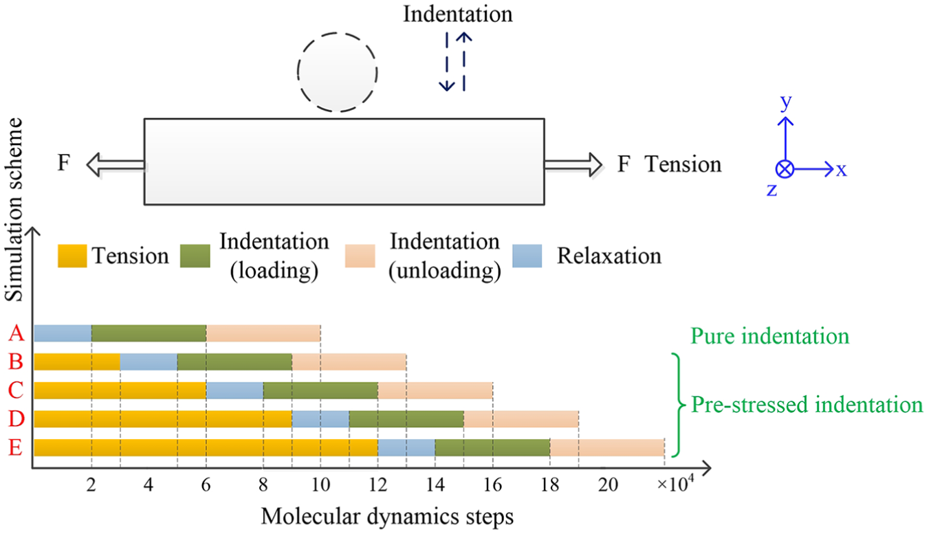
Sequences of molecular dynamics simulations and scheme for the nanoindentation process based on various TPD conditions.
The Large-scale Atomic/Molecular Massively Parallel Simulator (LAMMPS) MD program developed by Plimpton 27 was used to perform the large-scale three-dimensional MD simulations. The parallel computation was realized by using the Message Passing Interface (MPI) library. The common neighbour analysis (CNA) is adopted to identify the features of each atom and distinguish the lattice defect in the atomic structure. 28
Results and discussions
Material deformation under a variety of tensilepre-strians
Figure 3 shows the tensile results of monocrystalline copper and the local von Mises stress distribution at A, B, C and D points in the curve. As shown in Figure 3, the σ–ε curve can be divided into two stages: the elastic stage and the plastic stage. In the initial stage (ε = 0%–9%), or the elastic deformation stage, the stress increased with the strain in a linear manner. When ε increased to 9%, the stress suddenly decreased, and the monocrystalline copper entered into the plastic deformation stage. The stress at the peak of the curve (σmax) was defined as the yield stress (σb = 6.12 GPa), which corresponded well with the results reported by other researchers.29,30 After yield point, system stress decreased rapidly. In this article, we only study the nanoindentation response of monocrystalline copper under various tensile pre-strains in its elastic stage. Nanoindentation was conducted after the substrate stretched to a certain strain value, which corresponded to the special points of the curve in Figure 3, namely, A, B, C and D. As the snapshots shown in Figure 3, the stress distribution revealed that Von Mises stress expanded evenly in the substrate during tension process and higher stress occurred at larger tension strain.

σ–ε curve of monocrystalline copper under tension, including the local von Mises stress distribution at A, B, C and D.
Influences of TPD on material properties in nanoindentation
To evaluate the influence of deformation accumulation on the mechanical properties inside the monocrystalline copper substrate, a series of indentation tests at various TPD conditions were performed. These tests were eventually compared with the pure indentation simulation test under identical simulation conditions.
To create the tensile pre-stress conditions, the substrates were stretched to strain values of 0.012, 0.024 and 0.036. The local load–depth curves for nanoindentation, under the various TPD conditions, were obtained and shown in Figure 4 to be comparable with the pure nanoindentation curve. In contrast to the macroindentation curve, the nanoindentation curve contained fluctuation features due to the scale of the simulation.22,23 As shown in Figure 4, at the loading stage, the curve fluctuated around a constant value of ∼0.05 µN/nm. The fluctuations were caused by the relaxation of stresses in the system, such as lattice defects from the deformed states. Large drops of the force were most probably induced by the sudden release of elastic energy which accompanied with appearance of new dislocations underneath the indenter. Although the curves were relatively volatile, the trend was still clear. Since the indentation stress acted perpendicularly to the monocrystalline copper surface, the direction of contact shear stress beneath the indenter was identical to the tensile stress. The tensile stress increased the magnitude of shear stress. Moreover, it can also be explained from the energy perspective. As tensile pre-stress increased, the stored elastic energy rose. The increasing elastic energy resulted in higher potential energy in the crystal substrate. When the substrate situated a higher energy, a lower external energy would be introduced to realize the elastic or plastic deformation during indentation. Therefore, in the initial stage of loading curves shown in Figure 4, lower load was required in TPD for the same indentation depth compared to the stress-free.15,17,20 However, as the release of elastic energy exhausted, the energy in substrate tended to be consistent. Thereby, in the last stage of loading, the discrepancy in curves became smaller. As shown in unloading curves, the indenter suddenly lost ‘contact’ with the substrate atoms, resulting in a sudden drop of the load. The phenomenon in MD simulations of nanoindentation was reasonably explained in detail by Zhu and Fang. 31

Load–displacement curves for nanoindentation under various TPD and strain-free conditions.
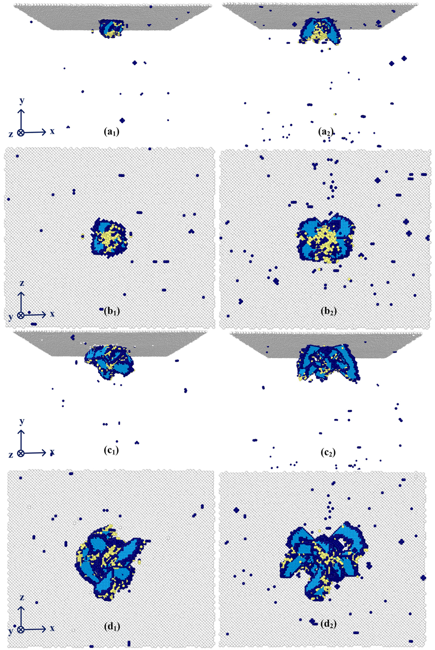
The surface physical properties, such as the hardness and recovery rate of the total work, and other mechanical properties are affected by many factors, including the initial temperature of the surface and the initial energy in the material. Usually, the initial thermal condition is presented by the kinetic energy distribution because the average kinetic energy can be transformed into the temperature distribution. The atomic potential energy and kinetic energy distributions of the substrate’s surface before indentation under a variety of TPDs are shown in Figure 5. According to Figure 5(a2)–(d2), there was no significant changes in the kinetic energy distribution on the indented surfaces, so the influential factors by different temperature distributions can be eliminated. The result implied that the re-relaxation stage after the tension process was well performed for the atomic kinetic energy on the surface returned to a low and stable situation. However, with an increase in elastic deformation, there was a significant increase in potential energy, as shown in Figure 5(a1)–(d1). As a result of TPD, both of the atomic position and atomic bonding changed with their increased separation; therefore, potential energy varied with TPDs. Furthermore, tensile stress caused an increase in stored elastic energy in the substrate, which would also lead to higher potential energy.
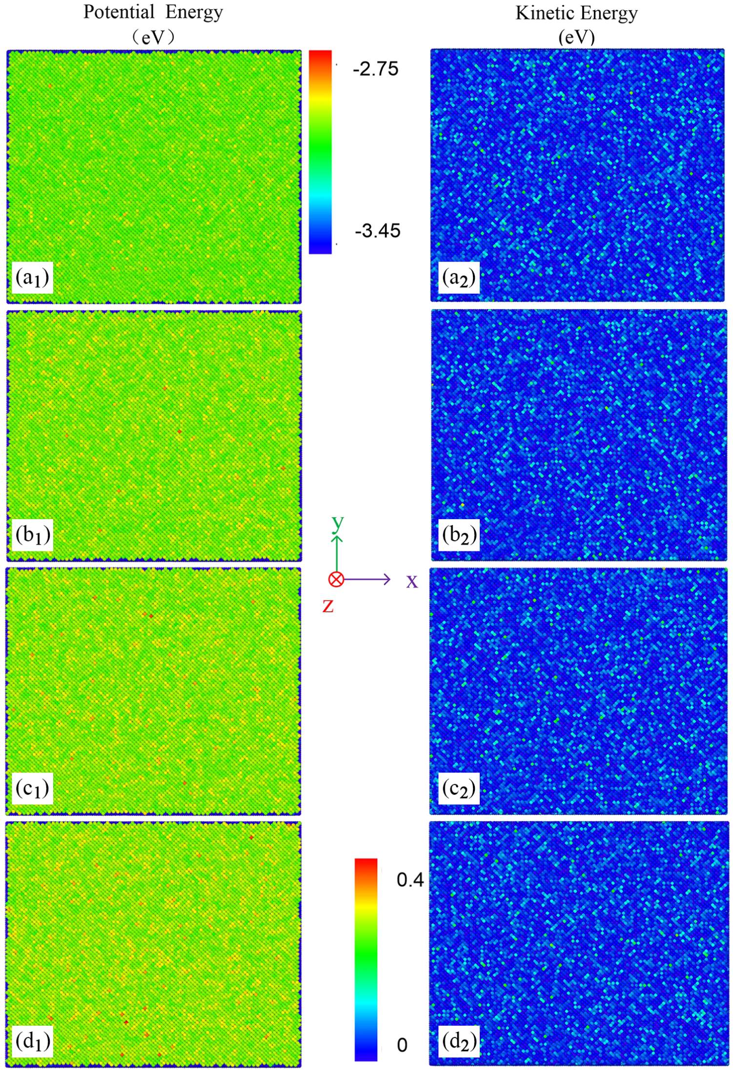
Atomic potential energy and kinetic energy distributions at the (010) surface before the indentation under a variety of TPD conditions. (a1) ε = 0%, (b1) ε = 1.2%, (c1) ε = 2.4%, (d1) ε = 3.6% and (a2)ε = 0%, (b2) ε = 1.2%, (c2) ε = 2.4%, (d2) ε = 3.6%.
According to the Oliver–Pharr method, 32 quantitative information, such as the hardness values, can be obtained from the P–h curve. The nanoindentation hardness H can be defined as follows
where Pmax is the maximum indentation load and Ac is the projected contact area, calculated using the following equation

where R is the radius of the indenter and h is the indentation depth.
According to equations (4) and (5), the hardness H under various TPD conditions was calculated as shown in Figure 6. With tensile pre-strain values of 0.012, 0.024 and 0.036, H was calculated as 8.89, 8.34 and 8.15 GPa, respectively. During the pure nanoindentation test, H was calculated as 9.68 GPa. Thus, the hardness decreased with an increasing TPD. From a microscopic perspective, the behaviour can be explained as follows: the interatomic distance increases with an increase in TPD, leading to a decrease in the bond energy of the atoms in the substrate, which results in a decline of hardness. Therefore, the surface strength with TPD conditions was lower than that in the pristine monocrystalline copper.
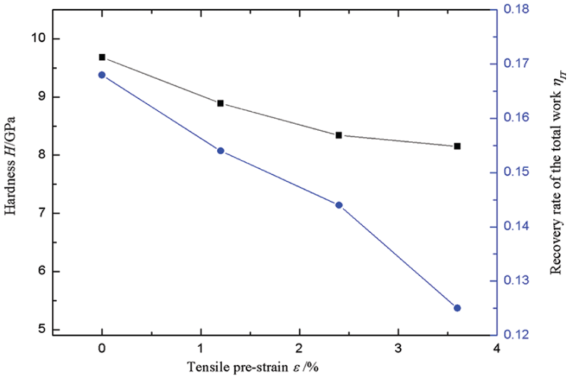
Variation of hardness and recovery rate of the total work during indentation at different TPDs.
The indentation loading curve can be described by Kick’s Law

where P and C are indentation load and loading curvature and h is indentation depth.
The indentation unloading curve is usually well approximated by the power law relation

where
The total work and the unloading work can be calculated by equations (8) and (9), where hmax denotes the maximum indentation depth and ηIT represents the recovery rate of the total work, as shown in equation (10). During the process of indentation loading, Wt translates into elastic and plastic work of the material deformation. During the unloading process, the elastic energy is released, whereas the plastic energy is stored in the form of residual stress in the material.
34
As is shown in Figure 4, the unloading curves shifted to the right as TPD increases. This resulted in an increase value hp in TPD conditions. It can be found from equation (10) that

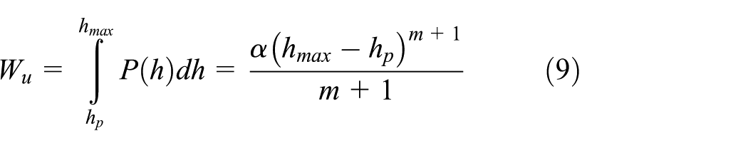
Based on equations (8) and (9), the recovery rate of the total work (ηIT) can also be obtained through integrating the loading and unloading indentation curves. ηIT for strain-free, 1.2%, 2.4% and 3.6% tensile pre-strain were calculated as 0.168, 0.154, 0.144 and 0.125, which are shown in Figure 6. As the single crystal copper has low yield stress, it behaves more plastically with small ηIT. With large elastic energy caused by TPD, the substrate will release more elastic energy in the indentation process; thus, it will lead to more plastic deformation and smaller recovery rate under the same loading conditions. The recovery rate of the total work, which covers 20 kinds of materials, has been researched and discussed by R Yang et al. 35 According to the ηIT values, the material can be divided into three categories: when 0.0 < ηIT < 0.3, the main materials are metal and alloy; when 0.3 < ηIT < 0.5, the main materials are metallic glass and ceramic; and when 0.5 < ηIT < 0.7, the main materials are ceramic. Therefore, ηIT can be used as an index for measuring the elastic-plastic deformation ability of materials. In the indentations of monocrystalline copper under pre-stress conditions, the ηIT values are in the interval of metal materials. The ηIT value depicted a decreasing trend as the tensile stress increased, which also suggested that tensile stress weakened the elastic deformation ability of monocrystalline copper. 36
The TPD affects the mechanical properties, as shown during the process of indentation. From the microscopic perspective, the mechanical property variations are due to the evolution of interior defects. Therefore, investigations into the nucleation and penetration dislocations are significant.
Snapshots of the instantaneous microstructure defects at different indentation depths with 1.2% tensile pre-strain are shown in Figure 7(a). It should be noted that these discussions presented here are not only based on the MD simulation snapshots but also based on the observation of the animations of indentation process. Perfect FCC atoms were eliminated for a clearer visualization of the damaged structures. Figure 7(a1) shows that at the penetration depth of 0.4 nm, the substrate was in its initial deformation stage, and the few defects were generated and distributed from beneath the indenter. Number 1 denotes the stacking fault of the local enlarged picture Figure 7(a2). They were distributed along a plane. As shown in Figure 7(a2) and (a3), the quantity of stacking fault increased with an increase in penetration depth. Number 2 denoted Shockley dislocation, which was on the border of the stacking fault and the FCC crystal structure. Shockley dislocation is a kind of partial dislocation. It can slip along the {111} crystal surface, which leads to the expansion or reduction of the stacking fault. Dislocation is a special atomic configuration, also known as a line defect, which can govern the mechanical properties of many crystalline materials, such as monocrystalline copper. The dislocation lines were extracted during the indentation step via the Dislocation Extraction Algorithm (DXA). Figure 7(b) is the internal dislocation line at different indentation depths and corresponds to the points shown in Figure 7(a). The dislocations were generated in the indentation contact area. According to Figure 7(b1)–(b3), Shockley dislocation played a dominant role in the process of indentation, while Hirth dislocation played a small role, which were generated at the edge of Shockley dislocations, as the penetration depth increased. No perfect dislocation was found because the atoms failed to achieve the required energy generation.

Instantaneous (a) atomic configurations, combined with (b) dislocation line evolutions during the indentation at 1.2% tensile pre-strain versus indentation penetration depth: (a1, b1) 0.4 nm; (a2, b2) 0.52 nm; (a3, b3) 0.6 nm. (a) Except boundary atoms shown in white, atoms inside the substrate are coloured according to CNA, as HCP atoms (green), BCC atoms (yellow), the other atoms (blue).(b) The DXA is used to assign dislocation, as Shockley dislocation (green), Stair-rod (purple) and Hirth dislocation (yellow).
In order to investigate the influence of pre-strain on atomic configurations during indentation, the atomic snapshots of substrate with strain-free and 1.2% tensile pre-strain at the indentation depth of 0.6 and 0.8 nm were selected, which is shown in Figure 8. The top view and front view are combined for a better perspective. In these snapshots, atoms in perfect FCC configuration were removed for clarity. In the different pre-strain conditions, the dislocations generated in the substrate all appeared along the inclined {111}-typed slip planes. However, compared with the substrate under strain-free (Figure 8(a1) and (b1)), more dislocations and stacking faults were generated in the substrate with tensile pre-strain (Figure 8(a2) and (b2)) at the same depth (0.6 nm). Furthermore, the following evolution of dislocations was also discrepant under different strain states. As shown in Figure 8(c) and (d), the dislocations in substrate with x-direction tensile pre-strain would like to be nucleated and developed in the same pre-strain direction at the depth of 0.8 nm. As the indentation depth increased, the phenomenon would be more striking, especially with larger tensile pre-strain. (The Supplemental Materials are shown in attachment.)
Snapshots of atomic configurations in substrate with strain-free and 1.2% tensile pre-strain at the depth of 0.6 and 0.8 nm with two different view angles: (a1, b1) with strain-free at 0.6 nm; (a2, b2) with 1.2% tensile pre-strain at 0.6 nm; (c1, d1) with strain-free at 0.6 nm; and (c2, d2) With 1.2% tensile pre-strain at 0.8 nm.
Suresh and Giannakopoulos 15 proposed a simple model to analyse the effect of residual stress on indentation. According to their model, a hydrostatic stress introduced by tensile pre-stress was in the same direction with the indenter loading and could be treated as an external indentation stress. The glide of dislocations in FCC crystals is commonly observed to obey Schmid’s law, whereby the applied stress is resolved onto the slip planes in the direction of slip. As the loading stress in indentation with tensile pre-strain is equivalently the actual indentation load plus an external stress, the dislocations would be generated earlier. Moreover, the dislocations and stacking faults preferred to be generated along the tensile direction.
Therefore, it can be concluded that tensile pre-strain can influence dislocation nucleation behaviour of material during the indentation.
Figure 9 shows the number of defective atoms obtained in the process of the indentation at various TPD conditions. There was a small discrepancy in the numbers of defective atoms, before the indentation, at various TPDs. As the indenter penetrated into the substrate, the number of defective atoms increased. The number of defective atoms at large TPD was higher than that at small TPD. During the initial stage (before the indentation depth of 0.5 nm), the substrate material underwent elastic deformation, and the number of defective atoms increased moderately. After the indentation depth of 0.5 nm, the number of defective atoms increased rapidly, which corresponded to the dislocation nucleation that occurred during the indentation.

Number of defective atoms during indentation at different tensile pre-strains.
Conclusion
In this article, three-dimensional MD simulations were constructed to investigate the nanoindentation response of monocrystalline copper under a variety of TPDs. We obtained the load–displacement curves from simulations of nanoindentation under various TPDs. The effects of TPD on the mechanical properties of monocrystalline copper, such as hardness and the recovery rates of total work, were calculated and investigated. The results showed that as the TPD increased, the hardness and the recovery rates of total work ηIT decreased, which suggested that the TPD would result in weakening of elastic-plastic deformation ability. The potential energy and kinetic energy distribution of the indented surface before indentation at various TPDs were also extracted, which further verified the fact that the parameter changes were due to different elastic energy caused by various TPDs. Furthermore, the atomic configurations were extracted to investigate the evolution of interior defects in substrate during indentation process. As the indenter penetrated the substrate, both the type and length of the dislocation line number increased. The results from nanoindentation on the surface with strain-free and 1.2% tensile pre-strain also revealed that tensile pre-strain could influence both the formation and development of dislocation in material during indentation: the dislocations and stacking faults in material with tensile pre-strain preferred to be generated more and developed along the tension direction. With the tensile pre-strain increased, the number of defective atoms during indentation also presented a growing trend.
This article provides a special MD simulation method for studying the mechanical response of materials under TPD, which is promising for applications in mechanical characterization of MEMS devices. Further analysis based on experiments will be completed in future research.
Supplemental Material
ADE1Supplementary_Material – Supplemental material for Nanoindentation response of monocrystalline copper under various tensile pre-deformations via molecular dynamic simulations
Supplemental material, ADE1Supplementary_Material for Nanoindentation response of monocrystalline copper under various tensile pre-deformations via molecular dynamic simulations by Lijia Li, Xingdong Sun, Yue Guo, Dan Zhao, Xiancheng Du, Hongwei Zhao and Zhichao Ma in Advances in Mechanical Engineering
Footnotes
Handling Editor: Jining Sun
Declaration of conflicting interests
The author(s) declared no potential conflicts of interest with respect to the research, authorship and/or publication of this article.
Funding
The author(s) disclosed receipt of the following financial support for the research, authorship and/or publication of this article: This research was supported by the Special Project for Development of National Major Scientific Instruments and Equipment (Grant No. 2012YQ030075), the National Natural Science Foundation of China (Grant No. 51275198 and 51505180), the National Natural Science Funds for Excellent Young Scholars (Grant No. 51422503), the Fund Guiding on Strategic Adjustment of Jilin Provincial Economic Structure Project (Grant No. 2014Z045), the Specialized Fund for Jilin Provincial Industrial Innovation Project (Grant No. 2016C030) and the Project of Jilin Provincial Young Science and Technology Innovation Leading Talent Team (Grant No. 20170519001JH).
Supplemental material
Supplemental material for this article is available online.
References
Supplementary Material
Please find the following supplemental material available below.
For Open Access articles published under a Creative Commons License, all supplemental material carries the same license as the article it is associated with.
For non-Open Access articles published, all supplemental material carries a non-exclusive license, and permission requests for re-use of supplemental material or any part of supplemental material shall be sent directly to the copyright owner as specified in the copyright notice associated with the article.