
Abstract
The cutting force generated during the cutting process affects the quality of the workpieces and tool wear. Accurate real-time monitoring of cutting forces plays an important role in the study of cutting mechanism and machining quality improvement. This article describes a tool with embedded nickel–chrome thin film sensor for cutting force measurement. The tool structure is optimized with grooving, drilling to form stepped sidewalls in the appropriate position. A simplified cantilever model for finite element simulation analysis in mechanics is used for analysis, in which the substrate thickness and Ni-Cr thin film–resistive grid position are determined through analysis. The output voltage is proportional to the external force with a factor of 0.0091 at 0.2 mm substrate thickness, which is a 100% gain over the original model. The designed tool with embedded sensors fabricated on the 0.5 mm substrate was validated with static calibration and cutting test. The results demonstrate that the sensor output voltage is proportional to the external force with a scale factor of 0.00518 and the resistance grid factor of 1.6. The tool and the Kistler dynamometer are in good agreement, with an error of 6.8% in measuring the main cutting force.
Keywords
Introduction
As a key parameter in the process of metal cutting, cutting force directly affects the quality of the workpieces and tool life. Accurate real-time and monitoring of the cutting force is instrumental in the study of the mechanism of the cutting process.
In recent years, we have seen steady progress in force sensor miniaturization and integration with the development in thin film deposition technology and micro electro mechanical system (MEMS). The Ni-Cr alloy thin film as a major force-sensitive material has been used in various types of force measurement. M Danisman and N Cansever made 500nm Ni-Cr alloy thin film strain resistance grid at the surface of glass sheet by magnetron sputtering (DC) and photolithography methods. The chemical composition and physical properties of the thin film strain resistance grid were studied, which gave a strain resistance grid factor value of 1.23. 1 C Taylor and SK Sitaraman 2 installed the Ni-Cr alloy thin sensor close to packaging solder bumps to measure the stress in packaging process. M Sohgawa et al. 3 fabricated a tactile sensor consisting of micro-cantilevers and Ni-Cr thin film strain resistance grid on the silicon substrate to detect the shear force in the sliding process.
However, embedded micro Ni-Cr thin film strain sensor in tools for measuring cutting force has not little studied. In this work, a tool with embedded Ni-Cr thin film sensor and modified tool shank structure was designed for cutting force measurement in machining process. Four Ni-Cr thin film resistance grids were connected to form a Wheatstone bridge as a sensor unit embedded in the redesigned tool shank. The redesigned model was analyzed with ANSYS workbench in mechanics to optimize the structural design. To get good output characteristics, the strain–external force relationship of the redesigned model is studied and reasonable arrangement of Ni-Cr thin film sensor as well as the substrate thickness is determined.
Analysis of force measuring principle
A cutting force measurement tool with embedded sensor is shown in Figure 1. The cutting force F can be decomposed into three orthogonal components: the main cutting force Fz, feed force Fx, and the radial force Fy. The strain gauge embedded in the tool shank surface for measuring cutting force in the cutting process is shown in Figure 1(a). Figure 1(b) shows a plane view of the tool whose tip is only subject to the main cutting force Fz. The height and width of tool shank are h and b, respectively. The tool is simplified as a cantilever beam fixed at one end. Y-axis is located the strain/stress neutral layer of the cantilever beam, and the Z-axis is parallel to the direction of the main cutting force Fz.R1–R4 are four strain resistance grids of the sensor unit.

Cutting force measurement with embedded sensor: (a) the components of turning tool force and (b) simplified model of the force measuring system and Wheatstone bridge connection.
The operation relies on converting the strain induced by cutting force in the resistance grid into an output voltage. Four strain resistance grids are connected to form a Wheatstone bridge as shown in Figure 1(b). The directions of two resistance grids R1 and R2 parallel the shank cross-sectional, while the directions of other two resistance grids R3 and R4 are along the longitudinal direction of the tool. The external force value can be measured according to the output voltage changes and the relative change in resistance ΔR1–ΔR4 caused by strain. If one assumes ΔR1 = ΔR2, ΔR3 = ΔR4, the output voltage of Wheatstone bridge can be expressed as

where k and ε are the resistance grid factor and strain, respectively.
The strain of cantilever beam fixed at one end is

where L is the distance between the center of four resistance grid and the tool nose, z represents the distance from the tool shank surface with the embedded sensor to the strain/stress neutral layer (Y-axis) of tool shank, E is the elastic modulus of resistor, and Iy stands for the moment of inertia of the tool shank cross section with regard to Y-axis, which can be expressed as

where a is the distance from any point of the tool shank cross section to the strain/stress neutral layer and A is the cross-sectional area of tool shank.
With equations (2) and (3), equation (1) becomes

In this article, we try to reduce the shank cross-sectional area A to improve the output characteristics without compromising the reliability. With reduced cross-sectional area, the strain as well as the output voltage becomes larger under the same machining conditions.
The system design
The cutting force measurement system consists of a tool system with embedded sensor and a signal processing system, as shown in Figure 2. The tool system includes a sensor unit, a tool blade, and a tool handle. The sensor is deposited on the bottom surface of substrate (AISI1045 steel) with DC magnetron sputtering. The substrate is screwed to the tool shank, which has a hole for the sensor wires to go through to the signal amplifier. Eventually, the collected data will be displayed in digital mode on the personal computer (PC).
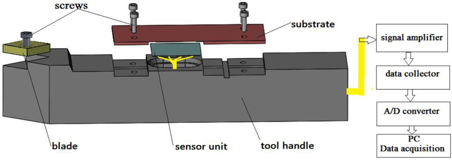
The cutting force measurement system.
Tool shank structure design
The redesigned tool shank structure, with cavities and holes near the sensor position, is shown in Figure 3. The width of each cavity is 0.6b, 0.5b, 0.4b in turn from surface down, with the height of each cavity set at 0.1h. Both ends of each step are rounded at the corners in order to reduce the stress concentration. Two identical cavities are machined in both (top and bottom) sides of the tool, with a hole connecting them. This hole is linked to an internal cavity that goes parallel with the length of the tool with an opening at the end of the tool. The sensor wires are lead through the above channel to the signal processing system.

The redesigned tool shank structure: (a) the tool shank 3D in sectional view and (b) dimensions of the tool shank cavities in cross-sectional view.
Simplifying the tool as a cantilever beam fixed at one end, the moment of inertia Im of redesigned tool shank cross section to the neutral layer Y-axis, as shown in Figure 3(b), can be expressed by

where Ii (i = 1–7) represents the moment of inertia of each cavity “slab” or the middle hole in the cross-sectional view with regard to the Y-axis. Thus, according to equations (3) and (5), Im = 0.48Iy.
By taking equation (5) into equation (4), the output voltage of redesigned tool becomes

According to formulas (4) and (6), under the same conditions, the ratio of the output voltage of the redesigned model to that of the original model is

Although the output voltage value is doubled with the change of tool structure, the tool strength must be considered as well. Selected the tool cutting edge angle kr = 45°, cutting edge inclination angle λs = 0, rake angle γ0 = 0°, the relationship between the cutting force F and its components are

If took Fz:Fy:Fx = 1:0.4:0.3 and F = 1000 N as a typical scenario, the three force components are

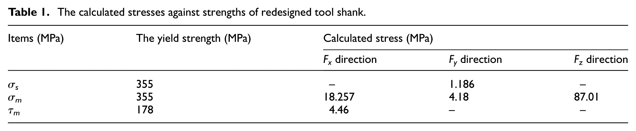
In this article, the reliability is measured by the following three stresses against corresponding strengths: tensile/compressive stress σs (induced by Fy), bending stress σm (induced by Fx, Fy, and Fz), and torsional stress τm (induced by Fx). With the cutting forces at 1000 N, the calculated stresses of the redesigned model as well as the yield strengths are shown in Table 1. All the calculated stresses are far below the limit, so the new design is feasible in terms strength at least. With the safety factor set to 2, the handle can well withstand 2000 N cutting force.
The calculated stresses against strengths of redesigned tool shank.
Sensor unit and substrate design
The sensor was fabricated as a thin film system consisting of a protective layer, strain layer, and an insulation layer on top of AISI1045 steel substrate, according to the dimensions illustrated in Figure 4. First, a 0.4 μm of silicon-nitride (Si3N4) membrane layer was deposited on the AISI1045 steel substrate as the insulation layer by plasma-enhanced chemical vapor deposition (PECVD). Next, the sensitive layer of Ni80Cr20 of 0.8mm thickness was deposited on the insulation layer using magnetron sputtering, the resistive grid and the electrode were patterned with photolithography in this layer. After that, as the protective layer, a 2-μm-thick silicon-nitride layer was deposited on the Ni80Cr20 thin film resistive grid area with PECVD and subsequently patterned to expose the contact window, onto which the gold wire was bonded finally as the electrode lead by hot pressing. The shape and size of resistance grid are shown in Figure 4(b): resistive grid (Ni80Cr20 film) length l=2mm and width bt = 0.05 mm, the number of stripes = 20. The resistivity of Ni80Cr20 resistive grid can be measured with four-probe method.
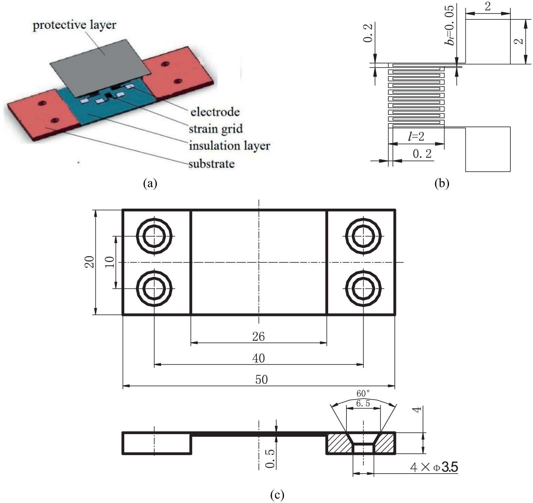
Schematic diagram of substrate and sensor: (a) the structure of substrate and sensor, (b) resistance grid shape and size, and (c) dimensions of the substrate.
The AISI1045 steel is preferred as the substrate material for its good adhesion with insulating layer as well as tool shank. As shown in Figure 4(c), the substrate area for sputtering deposition is 20 mm × 20 mm. There are four holes with a diameter of 2.5 mm in the substrate for the use of grooved cylindrical screw M2.5 to attach the substrate to the tool shank. In order to obtain a stable sensor, the root-mean-square (RMS) roughness of deposited substrate area needs to be less than 100 nm, so some of mechanical and chemical polishing methods are necessary to produce a high-quality substrate surface for film deposition.
Finite elements analyses
The software ANSYS workbench R14.5 is used for mechanical analyze of the redesigned model to look for the optimal location of sensor on tool shank. The material of tool shank and the substrate is AISI1045 steel, whose Poisson’s ratio and elastic modulus are 0.269 and 210 GPa, respectively. It is assumed that the material is linear, elastic, and isotropic. The total length of the tool shank is 125 mm and the clamping portion is 50 mm. The substrate thickness in sensor area is 0.5 mm.
The equivalent (Von Mises) stress cloud picture is shown in Figure 5. Compared with the case in original design, significant stress increase is found only around the groove position in the new design. The maximum stress value is under 98 MPa, which is way below the allowable value of 355 MPa of AISI1045 steel. The stress value is about 80MPa near the substrate center, well over the 40 MPa at the same position in the original design, as shown in Figure 5(b). Considering the linear relationship between strain and stress within the elastic range, the sensor output voltage Um would also increase if the grid is placed in the substrate center to get a higher strain.

The Von Mises stress cloud: (a) redesigned tool shank model and (b) original tool shank model.
The output characteristics of the sensor are gauged with the relationship between the strain of sensor and the external force of the tool. If the k and ε are known, the sensor output voltage can be obtained with formula (1). The value of k, which is taken as 2.0, here, depends on multiple factors including the Ni-Cr resistance grid thickness.1,4 The substrate strain at center in the Y-axis direction is taken as the sensor resistance grid strain ε. Figure 6 shows the simulated output voltage versus force in Z-axis direction for the two models.

Output voltage versus the external force in original and redesigned models.
As can be seen from Figure 6, the value of output voltage is proportional to the external force in both models. The slope ratio in the two models is 1.79, while it is about 2.08 in theoretical calculation. This difference may be attributed to the different thicknesses of substrate, which is not taken into consideration for theoretical calculation initially. By reducing the substrate thickness from 1 to 0.04 mm, higher output voltage is obtained, as shown in Figure 7.

Output voltage versus the substrate thickness under different loads.
Analyzing the data in Figure 7, the output voltage can be expressed with a fitting formula as follows

where t is the thickness of the substrate and c is the fitting parameter of the formula.
According to equation (10), the output voltage decreases with the increase of substrate thickness. This can be explained that the substrate thickness affects the distance between sensor grid to the tool shank neutral layer Y-axis and the moment of inertia of the tool shank section. There is an almost linear relationship between the output voltage and the substrate thickness for substrate thickness between 0.2 and 1 mm. When the substrate thickness is below 0.2 mm, the output voltage changes exponentially with it. It is possible that the substrate thickness is too small for the model to work properly. Considering the performance and stability of cutting tools and sensors, the substrate thickness is set to 0.2 mm, and the corresponding factor of the new design is 0.0091 while for the original model it is 0.0043. Thus, based on the simulations above, the output voltage of redesigned model has doubles compared with the original model under the same input condition.
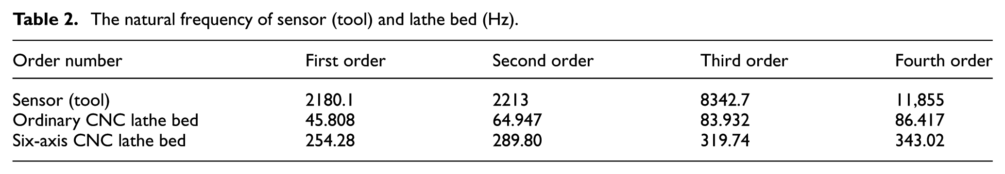
The vibrational behavior of the tool embedded sensor and lathe bed is also investigated. The tool natural frequencies of the first four order modes are analyzed by ANYSYS-workbench. It can be seen from Table 2 that the natural frequency of both ordinary computerized numerical control (CNC) lathe and six spindle CNC are far below the designed tool; it means that the vibrational behavior of the tool is viable in machining performance.
The natural frequency of sensor (tool) and lathe bed (Hz).
Sensor characteristics and experiment
Fabrication and parameters of Ni-Cr thin film sensor
As the key layer of sensor, 800 nm of Ni-Cr thin film was deposited on the Si3N4 layer which was pre-deposited on the AISI1045 steel substrate, as shown in Figure 8. The thickness of substrate is 0.5 mm. For Ni-Cr thin film deposition, the background vacuum is 1.5 × 10⁻⁴ Pa, deposition pressure is 1.0 Pa, and sputtering power is 100 W. The resistive grid pattern is formed with photolithography. The resistivity of Ni-Cr thin film is measured with a RTS-8 four-probe tester, and the resistance is measured with a HP34401A digital multimeter. Table 3 shows the measurement results.

Sample of sensor on AISI1045 steel substrate.
The Ni-Cr thin film measurement results.

Figure 9 shows the scanning electron microscope photo of cross section of Ni-Cr thin film sensor (×30,000). The thickness is 838.07, 874.12, and 802.02 nm at three different locations of thin film.

Cross section of Ni-Cr thin film sensor.
Sensor static characteristics and dynamic cutting experiments
The designed tool with embedded sensor is installed in the horizontal lathe C620, and the static response of the sensor is characterized by applying the load in Z direction at the tip. The stress and strain of the four resistance grids connected to Wheatstone bridge are collected using YD-15 type dynamic resistance strain gauge with an excitation voltage of 10 V, and the signal is transmitted to the DASP (data acquisition and signal processing)-36 channels. The system is shown in Figure 10.

(a) Cutting trial setup: (1) 40Cr workpiece, (2) the designed tool, (3) C620 lathe, and (4) Kistler 9272dynamometer. (b) Experimental setup for sensor calibration: (5) computer for data acquisition, (6) DASP (data acquisition and signal processing)-36 channel, and (7) YD-15 type dynamic resistance strain gauge.
The experiment process is to increase the weight hung to the tip of the tool holder step by step to 80 kg. As shown in Figure 11, the sensor output voltage is proportional to the external force with a scale factor of 0.00518, while the simulation result for this scale factor is 0.0077. The discrepancy may come from a lower factor k (<2) of the prepared resistance grid. The k calculated with formula (1) and Figure 11 is 1.6.

Senor calibration curves.
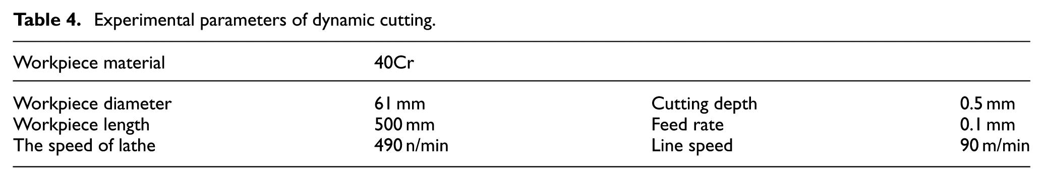
After the static calibration, the designed tool is mounted on a Kistler-9272 dynamometer for cutting trials, as shown in Figure 10(a). The cutting parameters are shown in Table 4.
Experimental parameters of dynamic cutting.
The main cutting forces in Z direction measured by Kistler dynamometer and calculated by the output voltage of designed sensor are shown in Figure 12. The results demonstrate that the tool and the Kistler dynamometer are in good agreement with an error of 6.8%.

Senor calibration curves.
Conclusion
We design a new model of the tool shank with an integrated sensor unit, which can be used for measuring cutting force in turning. The structure of the redesigned tool shank is simulated with finite element analysis, and the stress distribution under external force is analyzed to ensure the reliability. The structure and size of the resistance grid are designed. The location of sensor and the substrate center thickness are optimized. The tool shank and sensor are fabricated and the static and dynamic cutting tests of the tool measurement system are performed. The results validate the effectiveness of designed tool with embedded sensor in measuring main cutting force. More research and experiments will be focused on the triaxial cutting force measurement.
Footnotes
Handling Editor: Seung-Bok Choi
Declaration of conflicting interests
The author(s) declared no potential conflicts of interest with respect to the research, authorship, and/or publication of this article.
Funding
The author(s) disclosed receipt of the following financial support for the research, authorship, and/or publication of this article: The International Exchange and Cooperation Project, Shanxi, China (grant no. 2015081018).