
Abstract
This article proposed and discussed a kind of sigma-delta A/D converter for load cell signal acquisition, which uses improved charge balance technique. The traditional charge balance sigma-delta A/D converter is stable if and only if the magnitude of the input signal current is less than one half the magnitude of the reference current, which limits the accuracy improvement of load cell. This article examined the stability of an improved version of the charge balance sigma-delta A/D converter. The proposed converter can be designed to be stable for input signals as large as the reference, which is helpful to improve load cell’s measurement accuracy.
Introduction
The charge balance–based sigma-delta (SD) A/D converter is a well-known high-accuracy analog-to-digital converter, 1 which is used in measurement circuits of load cells, force transducers, and pressure sensors widely. Due to more and more high-accuracy requirement for weighing and force measuring, there are a number of research works focused on improving the A/D converters for higher measure precision,2–4 and some researchers also used it on different sensors.5,6 However, there is a limitation that the traditional charge balance A/D converter may be unstable during data acquisition under certain conditions. There have been several analyses and methods introduced to improve its performance,7–10 such as a closed-loop control system designed by Bharti et al. 9 to increase output voltage stability and a single opamp third-order SD modulator designed by Chao 10 for high-resolution applications. But all of these methods/architectures/models are complicated and expensive. This report discussed the design and theory of a novel improved converter. The proposed charge balance technique can achieve 24-bit performance, so it is suitable for low-level unipolar or bipolar signals in signal acquisition circuit of load cell, which can be overcome the limitation of traditional charge balance A/D converter.
Charge balance ΔΣ A/D converter
The proposed converter is identical to the traditional version except for one important attribute. Figure 1 is a schematic diagram that illustrates the improved charge balance technique. There is one component of the schematic in Figure 1 that differs from the traditional converter which is the voltage vramp that is used as the comparator reference. The traditional converter uses a constant voltage of 0 V as the reference, whereas vramp in the proposed converter is a saw tooth waveform (Figure 2). The slope of the ramp voltage is denoted by mramp (Figure 2). In all aspects other than the comparator reference voltage, the rules of operation of the proposed converter are identical to the traditional version. In both converters, the integrator capacitor is charged and discharged by isig and Iref during two phases, and the magnitude of the input voltage is determined from the measured lengths of the charging and discharging times. In the proposed converter, however, the transition between phases 1 and 2 occurs when the falling vout ramp crossed the rising vramp ramp, rather than when vout reaches 0 V. Figure 3 illustrates a typical conversion cycle. The variables (vi and vf) represent the initial and final values of vout for a single conversion cycle. The variable tx represents the length of phase one, and the total length of the conversion cycle is T0. The value of vout at the transition between phases is denoted by vx.

Simplified schematic diagram of proposed charge balance A/D converter.

Plot of saw tooth voltage used for comparator reference.

Graph of integrator output voltage during typical conversion cycle.
Analyses and discussion
Stability analysis in time domain
In Figure 3, the slopes of vout during the two phases are governed by isig and Iref that combine to form the total current into the capacitor. The integrator output voltage during phase 1,

Illustration of slopes of vout during typical conversion cycle.
For an arbitrary set of constant slopes msig, mref, and mramp, an equation may be obtained that relates the values of vi and vf. The first step is to obtain the following expressions for vx:

Equation (1) gives the value of vout at the end of a conversion period in terms of its value at the beginning of the conversion period when the input signal is constant. This equation may be used recursively to generate a sequence of peaks in vout that would result from an arbitrary initial value. The recursion can be written in a simpler form

The values of the peaks of vout are represented by v(k), and the constants b and c correspond to the following terms from equation (1)


Here, c is identical to the corresponding term in the difference equation for the traditional converter, but b is different. The above difference equation generates a sequence of values that converges to an equilibrium value when the converter is stable. All peak values of vout equal this value when the system is at equilibrium. The equilibrium value of peak voltage (ve) may be calculated from equation (2) for a given b and c by setting both v(k + 1) and v(k) to ve,
Figure 5 is a plot of vout during equilibrium for a hypothetical set of parameters for both the traditional and proposed converters. The figure also shows that the equilibrium peak voltage of the proposed converter is greater than that of the traditional converter for the same input signal. In fact, the function vout for the proposed converter is greater than vout of the traditional converter by a constant difference (vx) over the entire conversion period. This is a consequence of the equality of the corresponding slopes of vout for the two converters. Each converter used the same reference current, which determined the reference slope mref. The input current isig, which determined the slope msig, also is identical for the two converters for this example.

Comparison of conversion cycle for traditional and proposed converters.
In Figure 5, although the integrator output voltage is greater for the proposed converter, the time of the transition between the two phases (tx) is the same for both converters.
Because of the recursive manner in which peaks of vout are produced by the proposed converter in equation (2), there are certain conditions for which the converter is not stable. Successive evaluation of equation (2) using an arbitrary initial value v(0) yields the following

Equation (5) is an expression for the peak in vout after N conversion cycles, given that the input voltage is constant and that the value of vout at the start of the first cycle is v(0). As for both converters, the following condition must hold for stable sequences:

By following the same procedure, the corresponding stability condition for the traditional converter given (mref is negative) can be obtained
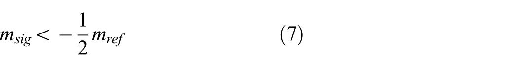
The inequalities of equations (6) and (7) differ only in the mramp term that appears in the equation for the proposed converter. The stability constraint of equation (7) requires that the input signal current isig be less than one half the magnitude of the reference current Iref for the traditional converter. However, the presence of the mramp term in equation (6) raises the limit of allowable input signal current for the proposed converter. Thus, the proposed converter can measure higher input currents than the traditional converter without becoming unstable.
If it is desired to measure currents as large as the reference current Iref, then equation (6) must hold for slopes msig as great as −mref. Substitution of this value for msig into equation (6) yields the following condition
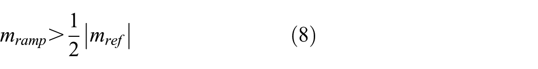
The inequality of equation (8) must be satisfied if the proposed converter is to be stable for input signals as large as the reference. In other words, the slope of the comparator reference voltage vramp must be greater than one half the magnitude of the slope mref if full-scale input signals (relative to the reference) are to be measured. If a suitably steep ramp is used, full-scale signals may be measured, that is, the proposed converter can be stable for duty cycles as high as unity.
Stability analysis in frequency domain
A frequency domain representation of the difference equation (2) provides additional insight into the stability of the proposed converter. A slightly different version of the equation is given as

Block diagram of difference equation.
The term z−1 in the figure denotes a unit delay. The input x[k] is assumed to be a step function of amplitude c, that is, x[k] = c u[k]. The sequence x[k] is used as an input to the discrete-time model only to supply the constant term c present in the difference equation. The output v[k] equals the sequence of peaks in vout produced by any initial value v[0]. The equivalent difference equation is given as

The system function of equation (9) has a pole at z = b. This pole is on the real axis because b is a real number (from equation (3)). Figure 7 is a plot of the poles and zeros of the system function.

Pole–zero plot of system function of equation (9).
As the figure indicates, the function has a zero at the origin. This single zero is a manifestation of the single unit delay in the output of the composite system. Poles and zeros at the origin reflect shifts in time, but they do not contribute to the magnitude of the system function; therefore, they do not affect the stability of the system. However, the location of the pole at z = b does affect stability. The magnitudes of all system poles must be less than unity if a system is to be stable; thus, all poles must lie inside the unit circle. This implies that the system of equation (9) is stable if and only if the magnitude of b is less than one, which is equivalent to the stability condition by time domain analysis. The location of the pole on the real axis of the z-plane may be expressed as a function of different parameters, including the various components of slope used in the foregoing analysis. Alternately, the pole location may be expressed in terms of relative input i and a system parameter K. The relative input is defined as the ratio of the input current to the reference current:
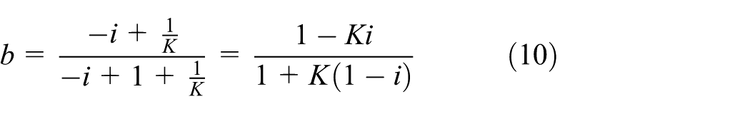
Equation (10) describes the pole location of the proposed converter. As noted in an analysis before, when K is less than or equal to two, the converter is stable for input signals as large as the reference.
As long as the slope mramp meets the requirement of equation (8), the converter will converge toward a state of equilibrium from any initial state. However, some characteristics of the convergence depend on the relative values of mramp and msig. In the examples shown in Figures 3–5, the ramp slopes mramp are greater than the signal slopes msig, but this is not necessarily true for all stable configurations. In particular, the ramp slope may be less than the magnitude of the reference slope:

Illustration of slopes of vout with signal slope greater than ramp slope.
The values of mramp and msig affect the convergence of the converter because they influence the value of the coefficient b of equation (3) that is used in the difference equation (2). As outlined in the preceding, b also specifies the location of the pole of the discrete-time system that models the converter. The following relationships may be derived from equation (3):
If
If
If
As the system converges, each successive vout peak draws closer to the equilibrium value than the previous peak. If b is nonzero, its sign determines whether vout overshoots the equilibrium value with each iteration. When

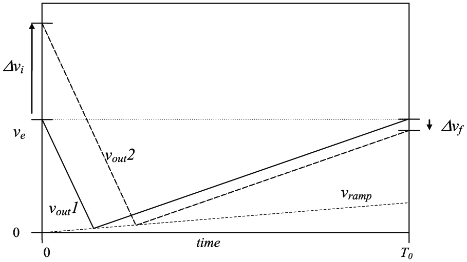
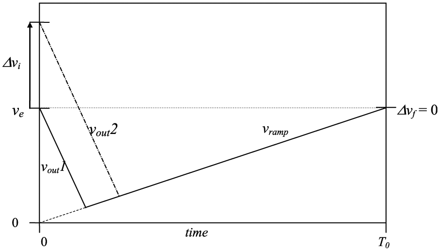
Conversion cycles with ramp slope greater than signal slope.
The figure depicts two different vout curves, vout1 at equilibrium and vout2 converging to equilibrium. Both the initial and final values of vout1 equal the equilibrium peak value, ve. The initial value of vout2 is greater than the equilibrium value by an amount denoted by Δvi. The peak value of vout2 at the end of the conversion period is also greater than the equilibrium value by the amount Δvf. The magnitude of Δvf is less than the magnitude of Δvi because the system is stable. Moreover, the sign of Δvi is the same as the sign of Δvf, indicating that vout2 does not overshoot the equilibrium value for this example. This is a consequence of the positive sign of b and the fact that the ramp slope exceeds the signal slope. The sequence of peaks of vout converges to the equilibrium value from above in this example. Figure 10 illustrates this process for several successive conversion periods.

Typical convergence with ramp slope greater than signal slope.
When the signal slope exceeds the ramp slope and b is negative, the peak value of vout overshoots the equilibrium value with each conversion cycle. This condition is illustrated in Figure 11.
Conversion cycles with signal slope greater than ramp slope.
Two different vout curves are shown again, vout1 at equilibrium and vout2 converging to equilibrium. The initial value of vout2 again exceeds the equilibrium value by Δvi, and the peak value of vout2 at the end of the conversion period differs from the equilibrium value by the amount Δvf. As shown in Figure 9, the magnitude of Δvf is less than the magnitude of Δvi, but the sign of Δvi is negative, indicating that vout2 overshoots the equilibrium value. This occurs because the ramp slope is smaller than the signal slope, causing b to be negative. The sequence of peaks of vout converges to the equilibrium value in an oscillatory manner in this example. Figure 12 illustrates this behavior for a few conversion periods.

Typical convergence with signal slope greater than ramp slope.
If the signal slope and ramp slope are equal, b is zero and there is no overshoot or undershoot. Convergence to equilibrium occurs in only one conversion period, as illustrated in Figure 13.
Conversion cycles with equal signal slope and ramp slope.
The fact that b is zero in this case causes the difference equation be reduced to the simple equation:
Conclusion
In this report, design comparison between traditional and proposed charge balance A/D converter is introduced. Then, stable analysis of a proposed charge balance A/D converter is discussed. The stable input limit formula is demonstrated both in time domain and frequency domain. For the traditional charge balance A/D converter, it is stable if and only if the magnitude of the input signal current is less than one half the magnitude of the reference current, and the proposed converter can be stable for load cell’s input signals as large as the reference. On the other hand, since this report limits the analysis on universal model, for which the metrics and parameters are not clarified, the proposed system model will be verified by experimental data in our future work. We believe that the proposed converter can provide better robust and signal-to-noise ratio for high-accuracy load cell signal acquisition.
Footnotes
Handling Editor: Mohamed Elhoseny
Declaration of conflicting interests
The author(s) declared no potential conflicts of interest with respect to the research, authorship, and/or publication of this article.
Funding
The author(s) received no financial support for the research, authorship, and/or publication of this article.