
Abstract
With the popularity of 5 G, there is an increasing request for a light, high-performance, and stable structure for wireless communication. To solve the problems of delamination cracking and its own heavy weight of the conventional microstrip antenna, this study used ultra-high molecular weight polyethylene (UHMWPE) filament tows and purple copper filament tows as raw materials to prepare 3D woven hollow structure microstrip antenna preforms on a common loom. Using the prepared preforms for reinforcement and resin as the matrix, the VARTM process was used to prepare a 3D woven hollow structure microstrip antenna with a height of 6.8 mm, a weight of 35 g, and a bulk density of 0.7 g/cm3. The combination of the electromagnetic performance test and HFSS software simulation shows that the antenna has excellent radiation performance with a gain of 7.5 dB and a measured VSWR of 1.25. The mechanical performance test results show that it can withstand a maximum compression load of 2982 N and a maximum bending load of 364 N with no obvious delamination at the fracture. It is light, thin, and load-bearing with excellent radiation performance. There will be great potential in the unmanned field and the space field in the future.
Keywords
Introduction
With the development of 5 G technology, antennas are increasingly becoming an important part of wireless communication. It usually consists of a radiation patch, a dielectric substrate and a ground floor.
1
Microstrip antennas have been widely used and researched because of their advantages of light weight, small size, thin shape, non-interference with aircraft aerodynamic performance, conformal structure and integrated design. The vast majority of existing microstrip antennas were laminated structures, as shown in Figure 1(a), the modularity of the laminated structure, flexible and easy to manufacture,2–4 but due to the different physical properties of each functional layer of the microstrip antenna, when the antenna structure was subjected to mechanical bending, stretching, or severe temperature changes, it was easy to delamination, and the mechanical properties were poor. In order to improve the bearing capacity of the antenna, a microstrip antenna with a honeycomb sandwich structure was designed. In order to improve the bearing capacity of the antenna, Tang et al.
5
designed a microstrip antenna with a honeycomb sandwich structure, as shown in Figure 1(b), the strength of the honeycomb structure was high, the density was low, and the upper and lower panels greatly improved the degree of bearing external pressure and impact.
6
However, the connection between the honeycomb core and the upper and lower panels was achieved by using adhesive bonding or careful splicing. 77,8 When the electromagnetic wave passes through the adhesive and the complex honeycomb structure, the energy is greatly attenuated.6,9 At the same time, due to the presence of the honeycomb core, which to a certain extent increased the longitudinal volume of the microstrip antenna, when the panel was subjected to flight load, it was easy to peel off and separate the panel. In order to improve the integrity of the microstrip antenna, Zhang et al.
10
used copper yarn and Kevlar yarn to weave a three-dimensional (3D) woven orthogonal structure of the microstrip antenna, as shown in Figure 1(c). The structure was woven by a 3D loom as a whole; the loom integrates the structure of the antenna and each element into one.
11
It avoided the drawbacks of layering and enhanced integrity and stability. However, the 3D woven orthogonal structure of the microstrip antenna dielectric substrate was thick and had a high dielectric constant, and its antenna gain was unsatisfactory. To reduce the weight of a microstrip antenna with a 3D woven orthogonal structure and improve its gain performance, Xu et al. studied a microstrip antenna with a 3D woven spaced structure in Figure 1(d) using glass fiber and carbon fiber covered yarn.
12
Although it achieved lightweight, it was difficult to form, it was necessary to manually paste the resin layer by layer to each yarn, its upper and lower panels rely on the yarn connection,
13
the yarn support was weak; and the surface of the panel was easy to collapse when it was impacted and compressed. Microstrip antenna structure (a) Laminated structure (b) Honeycomb sandwich structure (c) 3D woven orthogonal structure (d) 3D woven “8” spacing structure (e) 3D woven hollow structure.
In order to solve the problems of delamination, cracking, and overweight that may occur during the use of traditional microstrip antennas, this paper designed a 3D woven hollow structure microstrip antenna. The design used ultra-high molecular weight polyethylene (UHMWPE) filament tows and copper filament tows as raw materials, and the antenna was woven by using a common loom with an overall rectangular hollow structure. This structure was chosen because the lower the dielectric constant of the dielectric layer of the microstrip antenna, the lower the electric field confinement and the lower the energy loss, and thus the better antenna performance could be obtained. The dielectric constant of air is about 1, which is the lowest among common substances, and the higher the air content, the lower the dielectric constant and the better the electromagnetic performance. In the rectangular hollow structure, the upper and lower panels of the antenna were connected by fabric, and the connected fabric increases the carrying capacity of the antenna. The design made the antenna both excellent in electromagnetic performance and mechanical durability. The resonant frequency of the antenna was set to 2.45 GHz, which was suitable for Global Positioning System (GPS), telephone and other devices. The electromagnetic performance of the antenna was simulated and tested by using professional antenna software HFSS and an antenna measurement system.
Methodology
Development of design
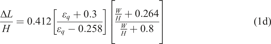
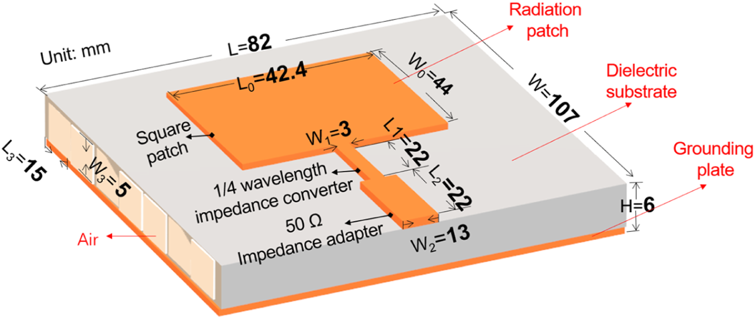
The radiation patch is an important part of the microstrip antenna radiation device, its main role is to convert the electromagnetic wave energy on the transmission line into free space radiation. The dielectric substrate is responsible for support and isolation, and its dielectric constant and thickness are directly related to the operating frequency, impedance, and bandwidth of the microstrip antenna, and other important characteristics. The grounding plate is used to close the circuit loop, effectively reduce radiation leakage, and improve radiation efficiency. Therefore, before weaving, the dimensions of each part of the 3D woven hollow structure microstrip antenna needed to be accurately determined, and the length and width of each part, including the length and width of the dielectric substrate, ground plate, square patch, 1/4 wavelength impedance converter, and 50 Ω impedance adapter, needed to be calculated using equations (1a) to (1h).
It was known that the height of the antenna was H = 6 mm, the length of the rectangular hole L3 = 15 mm, the width W3 = 5 mm, the speed of light C = 108, the center frequency fr = 2.45 GHz. The width W0 of the square patch could be calculated by equation (1a), and the length L0 could be calculated by equation (1b),
14
where the dielectric constant of the dielectric substrate εr, the effective dielectric constant εe and the line elongation Δl were derived from equations (lc) and (1d), respectively. The length L and width W of the dielectric substrate were obtained from equations (1e) to (1g), respectively. As shown in Figure 2, L1, L2, W1, W2 were calculated by the software TXline, where λg was the intra-dielectric wavelength and λ0 was the free-space wavelength. The antenna adopts 50 Ω impedance system with microstrip feed, and the impedance matching of the antenna was completed by quarter impedance transformation. ZC was the transmission line characteristic impedance, which was obtained by equation (1h),
15
where Zin was the input impedance and ZL was the load impedance. Antenna feed line width.

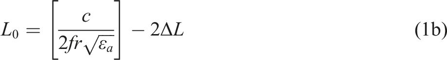


As shown in Figure 3(a), in order to check the accuracy of the calculation and accurately describe the performance of the 3D woven hollow structure microstrip antenna, a simulation model was built in Ansoft HFSS to further optimize the dimensions of the antenna to achieve the optimal preset effect. The result of software optimization is shown in Figure 3(b), when L0 = 42.4 mm, the center frequency of the antenna accurately reaches 2.45 GHz. the final design dimensions of the 3D woven hollow structure microstrip antenna are shown in Figure 4. HFSS optimization simulation. (a) Simulation model (b) Result of software optimization. Dimensional drawing of a 3D woven hollow structure microstrip antenna.
Assessment of design
As shown in Figure 5(a), the 3D woven hollow structure microstrip antenna preform consisted of three parts: radiation patch, dielectric substrate, and grounding plate. Through rational design, the whole weaving was done on an SGA 598 general loom, which was supplied by Jiangyin Tong Yuan Spinning Machine Co, the entire thickness direction was supported by plain fabric, the interlayer connection part was made of heavy flat tissue, and the three parts of the radiation patch, dielectric substrate, and grounding plate were woven integrally. This weaving method maintained integrity and stability, had better mechanical performances and damaged resistance. The 3D woven hollow structure microstrip antenna could withstand greater external loads, and greatly improved the integrity and forced the stability. Weaving diagram of 3D woven hollow structure woven microstrip antenna preform (a) Internal fiber diagram (b) Schematic diagram of single cycle yarn weaving.
Performances of UHMWPE filament tows and purple copper filament tows.

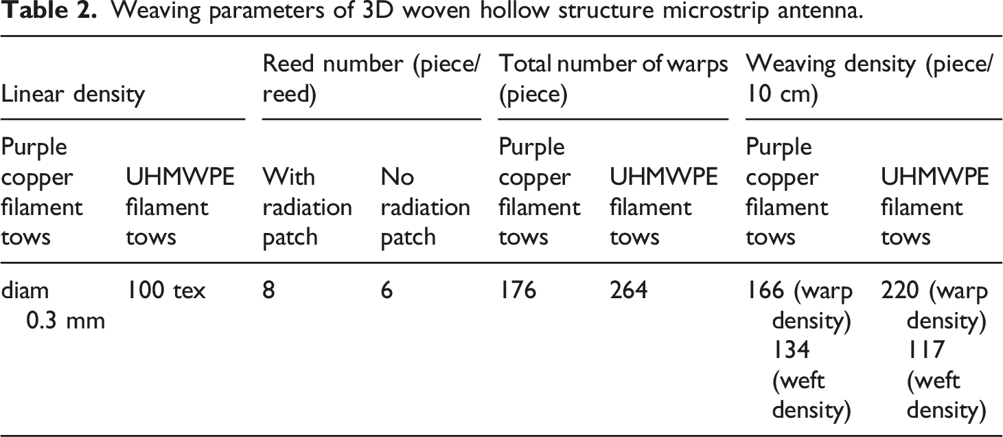
Weaving parameters of 3D woven hollow structure microstrip antenna.
As shown in Figure 6, mix the NO.1-692K-2/A resin and NO.1-692K-2/B curing agent evenly according to the weight ratio of 100:33, put the mixed resin in the vacuum box at room temperature, and defoam for 45 min. The preforms were immersed in resin using the vacuum assisted resin transfer molding VARTM process and then placed in an oven at 80°C and dried for 2 h.
17
The performance parameters of the resins used are shown in Table 3. Preparation process of 3D woven hollow structure microstrip antenna. Performances of NO.1-692K-2 epoxy resin.

3D woven hollow structure microstrip antenna test
Simulation and electromagnetic performances test of 3D woven hollow structure microstrip antenna
In accordance with the test standard GB/T 5597-1999 “Test method for complex permittivity of solid dielectric materials at microwave frequencies”, the dielectric constant of the dielectric substrate was tested using the waveguide method. In accordance with the test standard GJB 2038-94 “Methods for measurement of reflectivity of radar absorbing material”, an E8364B Agilent vector network analyzer provided by Kerui Electronic Instrument Equipment Co., Ltd. was used to test the return loss and standing wave ratio of the antenna. In accordance with GB/T 40602.2-2021 “Antennas and reception systems for interference-Part2: Basic measurement-Method for near field measuring high gain antenna pattern in microwave anechoic chamber”, using the microwave darkroom test antenna pattern.
In order to minimize errors during testing, certain requirements were needed for the testing environment. First, to reduce electromagnetic wave reflection, the test needed to be conducted in a reflection-free environment far enough away from external sources of interference, especially strong electromagnetic interference. Second, the appropriate temperature and humidity to ensure the accuracy of test results and the stability of the equipment. Finally, good ground conductivity to reduce reflected waves as well as the selection of a suitable test distance
Mechanical performances test of 3D woven hollow structure microstrip antenna
The universal material testing machine was used to test the compression and bending properties of the antenna specimens according to two strict standards: GT1448-2005 and GT/T1449-2005, respectively. The antenna was bifurcated into two specimens, namely a three-point bending specimen and a compression specimen. The former possessed an H-shaped structure with dimensions h = 6 mm, b = 15 mm, L = 136 mm, and l = 109 mm, while the latter was characterized by the following specifications: width 14 mm, thickness 6.80 mm, and height 19.65 mm. To ensure that the machine exerted a force within acceptable bounds, the pressure speed was moderated to 2 mm/min. Subsequently, the machine exerted pressure upon the antenna by the upper and lower indenters, thereby subjecting it to compression.
Results and discussion
Production of design
As shown in Figure 7(a), the weight of the 3D woven hollow structure microstrip antenna dielectric substrate was 8 g, which was less than the weight of two A4 sheets of paper. The UHMWPE filament tows were woven into a rectangular hollow structure. The height of the upper and lower panels was 6 mm, the hole height of the rectangular hollow structure was 5 mm, the air volume content was about 70%, and the bulk density was 0.34 g/cm3. As shown in Figure 7(b), the weight of the 3D woven hollow structure microstrip antenna was 35 g, which was equivalent to the weight of 6 one-dollar coins, and the bulk density was 0.7 g/cm3, which was very light and could be held up by a few green blades of grass. At the same time, we could see the fiber distribution inside the 3D woven hollow microstrip antenna, and the middle layer was connected by a tightly woven fabric of fibers. Compared to the sparse individual fibers in the middle layer of the “8” structure,
18
it could withstand the greater weight. A 3D woven hollow structure microstrip antenna weighing about 35 g can easily support a normal adult weighing 50 kg, as in Figure 7(c). The weight it could bear is 1428 times its own weight. A 3D woven hollow structure microstrip antenna was formed in one piece with light weight and good load bearing performance characteristics. Forming effect (a) Weight of dielectric substrate (b) Weight of 3D woven hollow structure microstrip antenna (c) Weight bearing effect.
Assessment of the design performance
Performance of 3D woven hollow structure microstrip antenna dielectric substrate
As shown in Figure 8(a), S11 = S22 and S12 = S21 of the 3D woven hollow structure microstrip antenna dielectric substrate, and the reflection coefficient (red line) of port 1 and port 2 were 0.1. The forward reflection coefficient from port 1 to port 2 and the reverse reflection coefficient (black line) from port 2 to port 1 were both 1. The energy loss of the dielectric substrate (blue line) was almost close to zero. The above results showed that the dielectric substrate made of UHMWPE filament tows and resin had the characteristics of low energy loss and good communication effect. As shown in Figure 8(b), the effective dielectric constant of the dielectric substrate was 1.48, and the dielectric loss value was 0.08.
6
The dielectric constant and dielectric loss were much lower than those of most solid composite structures and thus had excellent electromagnetic radiation performance. Test parameters of 3D woven hollow structure microstrip antenna dielectric substrate (a) S parameter and energy loss curve of dielectric substrate (b) Effective dielectric constant and loss tangent curve of the dielectric substrate.
Electric and magnetic field analysis of 3D woven hollow structure microstrip antenna
Unlike conventional microstrip antennas, the radiation patch and grounding plate of the 3D woven hollow structure microstrip antenna were formed by a conductive grid of interwoven purple copper filament tows, and the size of the gap between the yarns and the thickness of the yarns both affected the size of the interwoven grid and the electron propagation speed of the conductive part.
19
The electric field distribution of the 3D woven hollow structure microstrip antenna, Figure 9(a), the four corners and upper edge of the square patch had the largest field amplitude and the tail end of the 50 Ω impedance matcher had a relatively large field amplitude. The direction of the electric field emanated from the middle of the edge of the radiation patch and radiated around the perimeter of the radiation patch. From the magnetic field distribution of the 3D woven hollow structure microstrip antenna, Figure 9(b) showed that the strongest magnetic fields were found on both edges of the 50 Ω impedance adapter, followed by the strong magnetic fields on both edges of the square patch.
20
There was also a strong magnetic field at the connection of the 1/4 wavelength impedance converter to the square patch. The magnetic field direction radiated around the entire conductive part of the radiation patch. As seen from Figure 9, the edge of the radiation patch was the main part of the signal distribution and played a major role in the propagation process. Field distribution of 3D woven hollow structure microstrip antenna (a) Electric field distribution of 3D woven hollow structure microstrip antenna (b) Magnetic field distribution of 3D woven hollow structure microstrip antenna.
Simulation and experimental analysis of 3D woven hollow structure microstrip antenna
Return loss is the ratio of the power reflected back from the RF input signal to the power of the input signal, it is due to reflections from impedance mismatch, return loss will introduce fluctuations in the signal, and the returned signal is mistaken for the received signal, and confusion arises. From Figure 10(a), we could see that the simulated result of the return loss value was −18 dB at 2.46 GHz, and the measured result of the return loss was −19 dB at 2.7 GHz. The dimensional changes of the radiation patch in the process of weaving led to the deviation between the measured and simulated results in.21,22 When weaving the connection of square patch, 1/4 wavelength impedance converter, and 50 Ω impedance microstrip line, the width of the warp yarn (purple copper filament tows) needed to be cut according to the specific size, and because the cut purple copper filament tows were at the edge of the radiation patch, there would be a bump at the edge, and there would be a turn when the weft yarn was interwoven with the warp yarn, and its turn was controlled by a human, and the uncertainty was further increased, resulting in the unevenness of the edge of the radiation patch. Weaving errors and inaccuracies caused deviations in the size of the radiation patch, which further led to deviations in the preset resonant frequency from the measured resonant frequency. Electromagnetic performance of 3D woven microstrip antenna (a) return loss (b) Gain and efficiency curve (c) Standing wave ratio diagram (d) Smith chart (e) E-plane antenna pattern (f) h-plane antenna pattern.
As shown in Figure 10(b), the measured efficiency was 70% and the gain was 7.5 dB over the entire operating band, with the gain and efficiency appearing at a maximum near 2.7 GHz. The overall curve showed an upward trend, 2.7 GHz when the antenna’s actual operating frequency and resonant frequency match the most suitable. At this time, the antenna’s gain and efficiency reached the highest point. Instead of a smooth rise, the gain and efficiency curves of the antenna showed a ripple at 2.7 GHz.23,24 This was due to the change in impedance caused by the stretching of the purple copper filament tows during the weaving process and the unevenness of the edges of the radiating elements, both of which caused uncertain losses and interference as ripples in the gain and efficiency curves. Between 2.65 GHz–2.75 GHz antenna gain was around 7 dB or even more than 7 dB, the efficiency was more than 60%, which proved that the antenna band was still relatively wide. Meanwhile, as shown in Figure 10(c), the simulated VSWR of the antenna was 1.35 at 2.45 GHz. That was, the transmitting power of the antenna was more than 96%. The tested VSWR of the antenna was 1.25 at 2.7 GHz. That was, the transmitting power of the antenna was more than 98.3%. Simulation and test VSWRs were less than 1.5. Results showed that the feed line and antenna impedance were well matched, and the signal emissivity of the antenna was good even though there was some interference from weaving errors.
To maximize the signal source energy transfer, the impedance of the signal source must be equal to the conjugate impedance of the load, at which point the power transferred from the signal source to the load is maximized. The Smith circle diagram was generated by verifying the impedance matching of the load. 25 As shown in Figure 10(d), the Smith circle diagram simulated by HFSS deviated from the Smith circle diagram drawn from the actual measurement data, which may be caused by the fact that the purple copper filament tows became thinner and its impedance increased after being stretched during the weaving process. The amount of solder used when soldering the signal converter and antenna tail together was not calculable, which also resulted in an increase in impedance, further causing errors between the intended 50 Ω impedance match and the actual fabrication process.
The antenna pattern was the antenna radiation characteristics and spatial coordinates between the function of the graph. By antenna pattern could analyze the antenna space radiation characteristics. As shown in Figure 10(e), the radiation range of the main lobe of the measured antenna pattern E surface is concentrated in one direction,26,27 there is no secondary flap, and there is a small rear flap with the opposite direction of the main lobe. The overall antenna pattern E-plane matched the simulated one, and the simulated one had a larger radiation range than the measured E-plane antenna pattern. As shown in Figure 9(f), the main lobe direction of the measured and simulated antenna H-planes were the same, and the measured H-plane directional map had four small sub-lobes. The radiation range of the measured and simulated antenna patterns were about the same, which indicated the validity of HFSS simulation.
Comprehensive performance of microstrip antennas by structure.

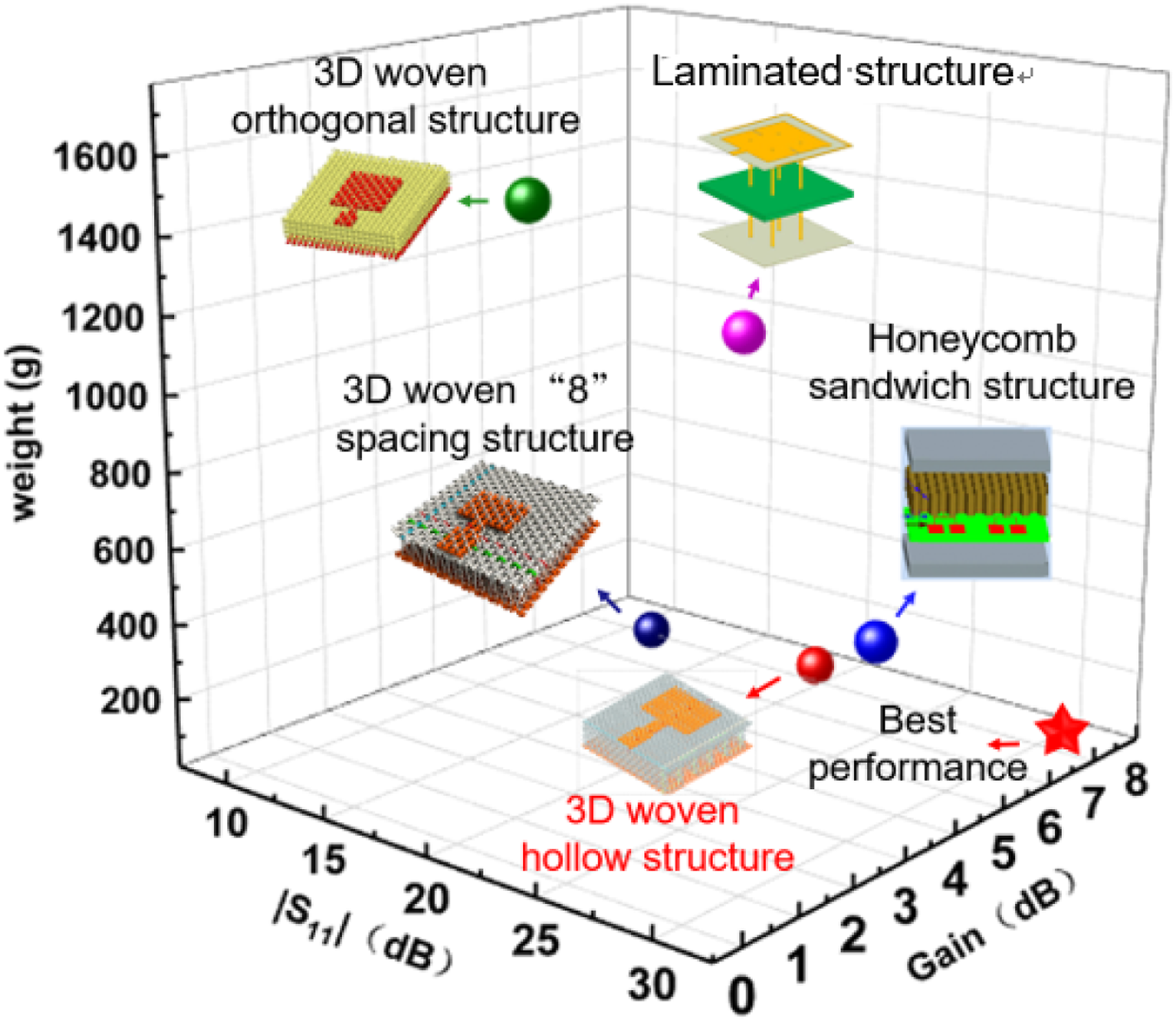
Comprehensive performance analysis of each structure microstrip antenna.
Radiation principle diagram of 3D woven hollow structure microstrip antenna
The radiation principle of microstrip antenna was actually electromagnetic leakage of high frequency. A microwave circuit not completely enclosed by a conductor will generate electromagnetic radiation at discontinuities in the circuit. As seen in Figure 12, the electric field between the radiation patch and the grounding plate included the electric field at the edge of the radiation patch and the electric field in the internal vertical direction. The internal vertical electric field oscillates back and forth with the sinusoidal changes of the alternating current but is always confined between the radiating patch and the grounding plate and does not radiate out. The only electric field capable of producing radiation was the fringe field of L0. Near the edge of the patch, the electric field only Y component, along the L0 side, in-phase adding together. And according to the transmission line theory, at this time, the front and rear edge of the electric field strength in the entire radiation patch was maximum, in favor of increasing the radiation strength of the antenna. 3D woven hollow structure microstrip antenna dielectric layer was hollow structure. The dielectric constant of the middle air layer was about 1, the lowest dielectric constant among common substances. The dielectric substrate with a low dielectric constant has small bondage to the electric field, which makes the edge field of L0 stretch farther along the Y direction, benefiting the antenna radiation. Radiation principle diagram of 3D woven hollow structure microstrip antenna.
Mechanical performances of 3D woven hollow structure microstrip antenna
The bending process is shown in Figure 13. The load-displacement curve in Figure 14(a) shows the load-bearing capacity of the sample. It exhibited obvious elastic-plastic characteristics.
31
The compressive load-displacement curve of the specimen was divided into three stages. In the first stage, as the upper indenter dropped, the overall force of the 3D woven microstrip antenna increased linearly in the load-displacement curve. Due to the overall stress on the sample, the microcracks generated by compression propagate through the specimen as a whole, causing local resin cracking. In the second stage, after the load reached the yield point of the 3D woven microstrip antenna, the load reached a peak of 2982 N. At this time, the resin stiffness was insufficient, and there were a lot of cracking and a small amount of fiber breakage. In the third stage, the 3D woven microstrip antenna was subjected to peak pressure. The fibers appeared to have a large number of fractures, the specimen damage deformation was obvious, and the load it could withstand plummeted, showing plastic deformation damage. In the subsequent compression process, the sample was stressed in the part not damaged by compression, and the curve decreased gently. The overall damage diagram of the specimen is shown in Figure 14(b). The fibers of the upper and lower panels of the specimen were broken and extracted at the connecting stems. The resin was cracked on the side, the UHMWPE filament tows on the front were deformed by compression, and the resin was discolored by extrusion. The purple copper filament tows on the back were obviously broken. The UHMWPE filament tows were also partially broken, and the resin was completely cracked. The overall performance of the 3D woven hollow structure microstrip antenna was good during the compression process without apparent delamination.
32
Process diagram of three point bending experiment. Mechanical performance analysis of 3D woven hollow structure microstrip antenna (a) Load displacement curve (b) Compression failure process (c) Three-point bending failure process.

As shown in Figure 14(a), the maximum load of the 3D woven hollow structure microstrip antenna was 364 N, and it could be seen from the curve that brittle damage occurred in the sample bending. The curve changed into three stages. As the upper indenter dropped, the upper resin and UHMWPE filament tows of the sample underwent compression damage, and the lower resin and purple copper filament tows underwent tensile damage.
33
The first stage curve rose smoothly until the maximum load was reached, at which point the purple copper filament tows at the bottom of the specimen was stretched and fractured by force. As shown in Figure 14 c1, the bottom purple copper filament tows underwent a brittle fracture. The UHMWPE filament tows did not break entirely but still had a portion attached. The load-displacement curve tended to fall and then rose after the second stage curve dropped linearly to the position of 250 N. At this time, the connecting stalk of the specimen was under tension, and the curve dropped. The upper panel was stressed when the connecting stalk was completely broken, and the curve showed a slight upward trend. At this point, the specimen was damaged, as shown in Figure 14 c2, with the filament tows and resin in the connecting stalk cracked, and a significant internal filament tows pullout occurred. In the third stage, the curve change tended to flatten out, the upper panel of the specimen was subjected to tension and pressure, the specimen was damaged, as shown in Figure 14 c3, and the resin was extruded and deformed. Comparing the damage diagram of the 3D hollow structure with that of the layered structure,
34
as shown in Figure 15, it could be seen that the 3D woven hollow structure microstrip antenna showed good integrity without delamination during the three-point bending. Damage diagram (a) The damaged diagram of 3D woven hollow structure (b) Damaged diagram of laminated structure.
Conclusion
In this study, a 3D woven hollow structure microstrip antenna prepare was integrated with purple copper filament tows and UHMWPE filament tows as warp and weft yarns, which had structural integrity and load-bearing capacity, weighing only 35 g with 67% air content, bulk density of 0.7 g/cm3, and height of 6.8 mm, which could easily bear the weight of an average adult, maintaining the load-bearing while achieved It is light and thin. The gain value of the 3D woven hollow structure microstrip antenna was 7 dB, which was much higher than that of the conventional microstrip antenna. In addition, the 3D woven hollow structure microstrip antenna had more than 98.3% transmit power under the interference of weaving error, and its electromagnetic parameters simulated and measured results were in good agreement.
The 3D woven hollow structure microstrip antenna showed great potential in aerospace applications with excellent electromagnetic performance and structural integrity. However, the purple copper wire selected in the experiment was easy to break when subjected to stretching, which led to a reduction in the overall mechanical performances of the antenna. In addition, the load carrying capacity of the rectangular hollow structure was relatively weak, and the frequency band of the microstrip antenna was narrow, which needs further improvement and optimization.
Footnotes
Declaration of conflicting interests
The author(s) declared no potential conflicts of interest with respect to the research, authorship, and/or publication of this article.
Funding
The author(s) disclosed receipt of the following financial support for the research, authorship, and/or publication of this article: This research was funded by the 2022 Basic Scientific Research Project of Liaoning Provincial Department of Education (LJKZZ20220064) and the Science and Technology Innovation Foundation(Science and technology benefiting people project) of Dalian(2022JJ13SN099).