
Abstract
The study of semiconductor materials under the combined influence of thermal, mechanical, and optical fields is critical for advancing nanoelectronic and optoelectronic applications. Traditional modeling approaches have largely relied on deterministic frameworks, which overlook the inherent randomness present in real-world systems due to thermal fluctuations, material heterogeneity, and environmental disturbances. This study aims to develop a comprehensive stochastic model for analyzing thermo-hydro-mechanical photoelastic interactions in poro-semiconductors, accounting for white noise effects. Using generalized photo-thermoelasticity theory, we incorporate hydromechanical coupling, pore pressure, and electron-plasma interactions in a fully saturated poroelastic silicon medium. The system of governing equations is solved analytically using Laplace and Fourier transform techniques to obtain deterministic and stochastic solutions. Variance analysis is employed to evaluate the effects of stochastic perturbations, and graphical comparisons highlight deviations between stochastic and classical deterministic responses. The results show that randomness significantly affects wave propagation characteristics, particularly in temperature, carrier density, displacement, and stress distributions. This research contributes a new theoretical framework for analyzing wave behavior under uncertain conditions, enhancing the reliability of semiconductor modeling. The novelty of this work lies in the integration of stochastic white noise, variance analysis, and hydromechanical coupling within a unified analytical model, which, to the best of our knowledge, has not been previously investigated in poroelastic semiconductors.
Keywords
Highlights
• Investigates wave propagation in piezo-photo-hygrothermoelastic semiconductors. • Incorporates temperature-dependent thermal conductivity into the model. • Analyzes the effects of nonlocality and hydrodynamics on wave behavior. • Utilizes the normal mode method for solving the governing equations. • Presents graphical results to illustrate the impact of key physical parameters.
Introduction
Studying stochastic photo-thermo-hydro-mechanical interactions in poroelastic semiconductors represents a convergence of multiple physical disciplines, including thermoelasticity, semiconductor physics, fluid mechanics, and stochastic processes. These materials, characterized by their ability to conduct electricity while exhibiting mechanical and thermal responses, are fundamental to modern nanoelectronics, optoelectronics, and energy-harvesting technologies. The interaction of optical, thermal, mechanical, and electronic fields in semiconductor structures is a highly intricate process, where temperature gradients induce stress waves, affecting carrier transport and fluid flow within porous media. The inclusion of stochastic effects (modeled through white noise fluctuations) adds a new dimension to this analysis, allowing for a more realistic representation of material behavior under uncertain conditions. This interdisciplinary overlap is crucial for advancing semiconductor technology, as real-world devices experience fluctuations due to laser excitation, environmental variations, and quantum-scale uncertainties. The ability to accurately model and predict wave dynamics in such materials has far-reaching implications in the design of MEMS, laser-assisted material processing, photothermal spectroscopy, and advanced sensor systems. By incorporating hydromechanical effects and stochastic modeling, this study enhances the understanding of wave propagation in semiconductor materials, providing a robust mathematical framework for future advancements in modern physics and engineering applications.
Thermoelasticity has experienced notable progress in recent years, especially with the integration of stochastic effects. Stochastic thermoelasticity examines the impact of randomness or uncertainty in material properties, external forces, thermal variations, and boundary conditions on the thermoelastic behavior of materials. This methodology is essential for comprehending the behavior of materials. Boit 1 proposed the notion of linked thermoelasticity to address the initial deficiency. The thermoelasticity is predicated on the classical Fourier heat conduction principle. Which asserts that a thermal wave moves at high velocities (infinitely) owing to the parabolic nature of the governing equation. This forecast may be appropriate for the majority of engineering applications. In specific situations, such as short-pulse laser heating operations, the traditional thermoelastic concept is physically insufficient. A hyperbolic model of thermoelasticity, which permits the thermal signal to propagate at a finite velocity, is more suitable for reproducing these phenomena. The Lord and Șhulman (LS) 2 model defined a singular relaxation time, while the Green and Lindsay (GL) 3 model integrates two relaxation times, which are prominent among generalized models. A multitude of studies have been undertaken based on these theories.
The initial photothermal technique was identified by Gordon et al. 4 when they saw an intracavity sample in which a laser device produced photothermal blooming, known as the photothermal lens. Kreuzer 5 subsequently demonstrated that photoacoustic spectroscopy may facilitate sensitive investigation with laser light sources. Photothermal techniques have been utilized to evaluate temperature, thermal diffusivities, sound velocity, bulk flow velocities, surface thickness, and specific heats.6–8 A multitude of authors have examined the photothermal generation that transpires throughout the photothermal interaction. The mechanism of this process in semiconductor materials consists of two elements: the propagation of a thermal wave generates elastic vibrations in the medium, which constitutes the thermoelastic (TE) mechanism of photothermal generation. 9 The energized free carriers generate a direct periodic elastic deformation, specifically electronic deformation (ED), within the sample. 10 A thorough theoretical examination of the thermoelectric (TE) and electrothermal (ED) effects in the semiconductors through a photothermal process necessitates forming intricate systems by concurrently examining the interconnected plasma, thermal, and elastic wave equations. 10 Technological advancements have resulted in the widespread application of semiconducting materials.
The theory of heat conduction in an elastic body, as developed by Chen et al.,11,12 is based on two temperatures: the conductive temperature and the thermodynamic temperature. Chen et al. 13 posited that the disparity between these two temperatures is directly proportional to the heat supplied. In the absence of heat supply, these two temperatures are equivalent in a time-invariant context. In time-dependent scenarios, particularly regarding wave propagation, the two temperatures in general exhibit differences, irrespective of heat input. Recently, a lot of considerable scholarly given great attention to the theory of two-temperature thermoelasticity. Qiu and Tien 14 have demonstrated the existence, structural stability, convergence, and spatial characteristics of two-temperature thermoelasticity. Youssef 15 has formulated a novel model of generalized thermoelasticity predicated on two temperatures, wherein the disparity between these temperatures is directly proportional to heat input, governed by a non-negative constant a (length). Youssef and Al-Lehaibi, 16 along with Youssef and El-Bary, 17 investigated various aspects of two-temperature thermoelasticity with relaxation durations, revealing the findings differ in a qualitative form from those related to one-temperature thermoelasticity. Marin et al. 18 introduced a finite element approach to analyze nonlinear bioheat transfer in skin tissue, emphasizing the impact of external thermal sources. Their work is particularly relevant to photothermal interactions in biological systems, drawing parallels with laser-induced heating in semiconductor materials, where thermal waves and stress interactions must be accurately modeled.
Kumar and Devi 19 explored thermomechanical interactions in porous generalized thermoelastic materials with internal heat sources, which aligns closely with poroelastic semiconductor behavior, where fluid saturation, heat conduction, and mechanical coupling play a crucial role in wave dynamics. Their research helps to understand how thermal gradients influence material deformation, similar to the photo-thermoelastic responses observed in semiconductor structures. Bachher et al. 20 investigated fractional derivative heat transfer in a generalized thermoelastic infinite medium with voids, considering an instantaneous heat source. Their study provides insight into thermal wave propagation in porous materials, which is directly applicable to stochastic heat diffusion and plasma-electron interactions in semiconductor devices. Ailawalia and Singh 21 examined the effect of rotation in a generalized thermoelastic medium subjected to ramp-type heating and hydrostatic initial stress. Their findings on rotational and thermal effects in deformable materials complement the present work by reinforcing the importance of hydromechanical and thermal coupling in wave propagation through semiconductor structures. Tiwari and Kumar 22 explored nonlocal effects in micro-mechanical resonators using a three-phase-lag thermoelasticity model with memory-dependent derivatives, highlighting nonlocal interactions in small-scale systems. Their study is relevant to nanoelectronic semiconductor applications, where nonlocal and stochastic effects become dominant in governing material behavior. In another work, Tiwari et al. 23 studied thermoelastic vibrations of nanobeams under varying axial loads and ramp-type heating, applying the Moore-Gibson-Thomson generalized thermoelasticity theory. Their contributions are valuable in understanding nano-scale semiconductor wave interactions, where thermal, mechanical, and photonic excitations interact under stochastic conditions. The study investigates the transmission of photoacoustic waves in thermally stimulated materials, emphasizing the interplay between thermal and mechanical waves. 24 Advanced models include microtemperature effects and elasto-thermodiffusion theories to examine the behavior of semiconductor materials under photothermal excitation. 25
Lotfy et al. 26 use photo-thermoelasticity theory to study plasma-mechanical-elastic wave stochastic propagation at the boundary of an elastic half-space in a semiconductor material. Integrating stochastic simulation with temperature-dependent electrical conductivity and variable thermal conductivity to a 2D electromagnetic. White noise is used as the randomization element in this work, which better depicts semiconductor material random processes than previous research. Li et al. 27 used the robust explicit time-domain method (ETDM) for structural random vibration in the stochastic analysis of coupled thermoelastic issues. Deterministic impulse response analysis formulates explicit time-domain representations of critical responses to solve stochastic evolution equations. Then, explicit formulas enable efficient random system response statistics computation. Thus, ETDM addresses the physical and stochastic evolution mechanisms separately. This makes the approach ideal for stochastic Multiphysics issues such as thermoelastic vibration, characterized by intricate physical mechanisms. Sakata 28 analyses a composite material thermoelastic issue using stochastic homogenization. The stochastic homogenization approach is first formulated using thermoelastic homogenization theory. The stochastic homogenized thermal expansion coefficient of a unidirectional fiber-reinforced composite material is studied for minor random variations. Stochastic composite materials with an isotropic porous matrix reinforced by disoriented ellipsoidal inclusions with orthotropic symmetry in thermoelasticity were studied by Nazarenko et al. 29 Stochastic heating on an elastic material described as an endlessly long circular cylinder subjected to a penetrating substance on its outer surface is studied by Allam et al. 30 Stochastic heating and random properties of the material resulted from additive Gaussian white noise. Sherief co-authors as 31 investigated a thermoelastic half-space issue within the framework of the generalized thermoelastic diffusion. Gupta 32 studied the interactions utilizing the dual-phase-lag thermoelasticity model under the stochastic boundary conditions. Alenazi et al. 33 investigated moisture diffusivity on an elastic semiconductor material using a stochastic heating technique. Where random processes are carefully implemented at semiconductor media boundaries. Recent advancements in photothermal and thermoelastic modeling have explored the complex interactions between thermal, mechanical, and optical fields in semiconductor and nanostructured materials. For instance, Abouelregal et al. 34 investigated the photothermal-induced interactions in a semiconductor solid with a cylindrical gap under the effect of laser pulse duration, employing a fractional Moore-Gibson-Thompson (MGT) heat conduction model. Their study provided deeper insights into how fractional-order derivatives influence heat transfer in semiconductor structures. Additionally, Abouelregal et al. 35 examined the temperature-dependent characteristics of rotating nonlocal nanobeams subjected to a varying heat source and a dynamic load, highlighting the effects of nonlocality and rotation on the material’s thermomechanical response. These studies demonstrate the significance of incorporating fractional and nonlocal theories in analyzing semiconductor materials, further reinforcing the necessity of our current investigation into wave propagation under coupled photothermal and hydrodynamic effects.
Recent studies have extensively investigated the fluid dynamics and hydraulic performance of axial and centrifugal pumps under various operating conditions using both experimental and computational approaches. Al-Obaidi and Alhamid 36 analyzed the internal flow characteristics in axial pumps by employing a varying frequency vibration technique, providing valuable insights into flow instabilities. Their subsequent work 37 examined the impact of blade number variations on unsteady flow patterns, demonstrating the influence of pump geometry on performance. Computational fluid dynamics (CFD) and acoustic analysis have also been used to evaluate hydraulic efficiency and cavitation effects, 38 highlighting the role of transient loads in altering flow structures within axial flow pumps. 39 Further, Al-Obaidi 40 investigated the effect of guide vane configurations on the flow field, offering optimized designs for improved performance. In centrifugal pumps, the rotational speed significantly affects cavitation formation and detection, as shown in studies based on vibration and acoustic diagnostics.41,42 Moreover, pressure fluctuations and blade angle variations play a crucial role in unsteady flow dynamics, influencing pump stability and efficiency. 43 These studies contribute to a deeper understanding of fluid-structure interactions and vibrational characteristics in hydraulic systems, aligning with our research focus on wave propagation and dynamic response in semiconductor materials under hydrodynamic conditions.
In recent years, extensive research has been conducted on thermoelastic and photoelastic interactions in semiconductor materials. However, most existing studies have focused on deterministic models, neglecting the inherent stochastic nature of thermal and mechanical fluctuations in real-world applications. This study introduces a stochastic framework to investigate thermo-hydro-mechanical photoelastic interactions in poro-semiconductors, incorporating white noise effects to model uncertainties in the system. The novelty of this study lies in the development of a stochastic photo-thermo-hydro-mechanical model for wave propagation in poroelastic semiconductors that incorporates white noise effects—an approach not previously addressed in the literature. Unlike conventional deterministic models, this work introduces stochastic boundary conditions and utilizes Wiener processes to simulate random thermal and carrier fluctuations, leading to a more realistic representation of semiconductor behavior under external excitation such as laser heating. The combination of hydromechanical coupling, stochastic thermal dynamics, and variance-based analysis within a unified analytical framework using Laplace and Fourier transforms offers new insights into wave propagation, variance evolution, and energy dissipation. The proposed model overcomes the limitations of previous deterministic approaches by incorporating randomness in the boundary conditions, but it is constrained by the assumption of linear material behavior and Gaussian white noise processes, which may not fully capture complex semiconductor interactions under extreme conditions. The key advantages of this model include its ability to predict realistic wave propagation under uncertain conditions, improved accuracy in modeling semiconductor performance under laser heating, and better insight into carrier-transport mechanisms in porous semiconductor structures. The results indicate that stochasticity significantly influences thermal and mechanical responses, with variance behaving in an exponential decay form, suggesting a crucial role in designing semiconductor-based systems. This framework has broad applications in semiconductor technology, including optoelectronic devices, laser-assisted material processing, photothermal spectroscopy, energy harvesting, and microelectromechanical systems (MEMS). To the best of our knowledge, this is the first model that integrates these complex physical interactions under stochastic influences, thereby providing a foundational tool for the design and analysis of robust semiconductor devices in nanoelectronics, MEMS, and optoelectronic systems. The findings are particularly relevant to nanoelectronics and sensor technologies, where random thermal and electronic fluctuations play a critical role in device performance and reliability. This study provides a robust mathematical foundation for future research on stochastic wave dynamics in complex semiconductor structures.
Mathematical model and basic equations
Without the external forces, the electro-thermo-hydro-mechanical model of a half-space saturated poroelastic semiconductor medium is

Such that, the thermal activation coupling coefficient is (ii) The equations of motion for an elastic semiconductor material with hydromechanical coupling is8,48 (iii) The heat equation of poroelastic semiconductor material with photo-hydro-hydromechanical theory is39,49 (iv) The equation of mass conservation for water is
50


The constitutive equation of thermo-hydro-mechanical theory without body force or internal heat source is51,52


The displacement-strain is

Expanding equations (2) and (5) as follows:


The electronic deformation coefficient is
In this study, several key non-dimensionless quantities are introduced to enhance the mathematical formulation and physical interpretation of the problem. These quantities play a crucial role in capturing the complex interactions between physical fields within the semiconductor medium. By incorporating these parameters, we aim to provide a more generalized analysis that accounts for the inherent physical scales of the system. The selected non-dimensionless quantities facilitate a comprehensive understanding of wave propagation, thermal effects, and coupled interactions, ensuring that the theoretical framework remains applicable to a wide range of practical scenarios. The specific quantities considered in this work are as follows
53
:
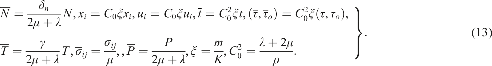
Incorporating the previous quantities in equations (1), (3), (4), and (8)–(12), we get the following equations:


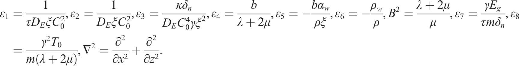
Such that,

The problem solution
The method of Laplace and Fourier is used for solving. Define Laplace transform as54,55

Then defining Fourier transform as

Applying the previous transforms on the equations (14)–(20) yields


Excluding


The (O.D.E.) equation (32) can be rewritten as

The linear solutions after applying Laplace and Fourier are:


From equation (22), the component of the displacement can be obtained after applying Fourier and Laplace transforms as

The mechanical stresses components are


Boundary conditions
To obtain the values of (1) In this study, we impose a thermal shock boundary condition to simulate the rapid and localized temperature change at the surface of the semiconductor material. A thermal shock represents an instantaneous or highly transient heat pulse applied to the boundary, which induces significant thermal gradients and affects the wave propagation characteristics within the material. A thermal shock boundary condition that can be chosen as8,40

Such that (2) In hydro-poroelastic materials, such as nanoporous silicon or semiconductor membranes, surface pores are often exposed to ambient conditions, leading to minimal external pressure effects. In this study, we assume a free water pressure boundary condition, meaning that the water pressure at the boundary is negligible or zero. This assumption is commonly used in hydro-poroelastic semiconductor models where the surface is exposed to an open environment or fluid interaction without significant external constraints. The water pressure can be taken as

In our model, we adopt the free water pressure condition to simplify the analysis and focus on the intrinsic wave propagation characteristics within the hydro-poroelastic semiconductor medium. This assumption provides a reasonable approximation for many practical scenarios while maintaining computational efficiency. (3) In this study, the boundary condition for carrier density of charges is modeled considering the recombination process at the semiconductor surface. This assumption is crucial in semiconductor physics, as charge carriers (electrons and holes) naturally undergo recombination due to interactions with defects, impurities, and external influences. The carrier density of charges is

Such that ( (4) In this study, we assume a free normal stress boundary condition, meaning that the normal stress at the surface of the semiconductor medium is zero. This assumption is widely used in wave propagation and elasticity problems, where the surface is not subject to external mechanical constraints or applied loads. The normal boundary condition for stress can be expressed as

In our model, the free normal stress boundary condition is chosen to simplify the mechanical analysis while capturing the fundamental elastic wave behavior in the semiconductor medium. This assumption provides a reasonable approximation for many practical scenarios, particularly in wave propagation studies.
Applying Laplace and Fourier transform to the equations (43)–(46), it becomes:


Inversion of Laplace and Fourier transforms
To derive the problem solutions in
First, the Fourier inverse of an arbitrary function

Then the Laplace transform is inverted as
42

These analyses confirm that the transformed equations remain well-posed and yield physically meaningful solutions when inverted back to the original domain.
In our study, we introduce stochastic elements to model random fluctuations in the semiconductor medium, particularly in electrical conductivity and carrier dynamics. To address these elements: • We employ random perturbations in the governing equations, assuming a white noise distribution to model uncertainty in charge carrier transport. • The statistical properties of the stochastic process are preserved through the transformations, allowing us to track how randomness influences wave propagation. • The transformed system provides a deterministic framework for analyzing stochastic effects, enabling us to compute mean values and variances of wave parameters.
By incorporating stochasticity into the formulation, we provide additional insights into the realistic behavior of semiconductor materials under fluctuating external conditions.
Incorporating Wiener processes into the stochastic formulation allows us to model random fluctuations in carrier density, electrical conductivity, and thermal properties. These stochastic elements introduce uncertainty in wave propagation, altering the dispersion characteristics and modifying energy dissipation rates. The presence of random fluctuations broadens the spectral components, influencing wave attenuation and stability under certain conditions. Compared to deterministic models, the inclusion of Wiener noise leads to a probabilistic response, necessitating expectation value and variance analysis for meaningful physical interpretation. Additionally, the effect of stochasticity on boundary conditions introduces time-dependent perturbations that influence thermal and mechanical responses at interfaces. While Wiener processes effectively capture short-term fluctuations, other models such as Ornstein-Uhlenbeck processes could be considered for memory-dependent effects. This approach provides a more realistic representation of semiconductor behavior, particularly in nanoelectronics and optoelectronic applications, where random thermal and charge carrier variations significantly impact system dynamics.
The temperature distribution in the physical (space-time) domain
Deterministic temperature
Making the use of the equation (35), the deterministic temperature is

Defining the temperature boundary of equation (39) as
32

Stochastic temperature
In our mathematical model, we employ a series of transformations to reduce the complexity of the governing equations and facilitate their solution.
Defining the temperature boundary with the random function


Since the stochastic process is taken as white noise type and it satisfies the following property for any stochastic process

After inserting the random term

Next, equation (53) may be rearranged as

Inserting equation (55) into the above equation, we get


Inverting the Fourier and Laplace transform into the above equation and using the convolution property of Laplace we have:

Now equation (62) is written as

Recalling another Laplace’s property related to the autocorrelation as46,59

Such that

For a stationary function, the autocorrelation is just a function of the time interval alone as
32

From equations (53) and (65) we get


Since

From (66), the double Laplace transform of (69) is

Some properties of the double Laplace transform are46,47 • •
Using the previous properties, equations (68) and (70) give:


Putting above

Replacing

Carrier density distribution in the physical (space-time) domain
Deterministic carrier density
The deterministic carrier density takes the following form after utilizing equation (37)

Stochastic carrier density
Using the property of equation (56), and the above equation, the mean of the carrier density is the same of the deterministic one as

From equation (72), the carrier density field takes the following form:

Inserting equation (55) into equation (74) we get33,43–45

Applying the same steps used in temperature distribution, we get

Then, the Variance is

Excess pore water pressure field
Deterministic excess pore water pressure
The deterministic water pressure can take the following form after utilizing equation (37)

Stochastic water pressure
Using the equation (56), and the above equation (78), the mean of the water pressure is the same as the deterministic one as

From equation (36), the deterministic water pressure distribution field is48,49,60

Inserting equation (55) into equation (83), we get

Applying the same steps used above, we get

Then, the Variance is

The displacement distribution
The deterministic displacement distribution
The deterministic displacement can take the following form after utilizing equation (40)

The stochastic displacement distribution
Using the equation (56), and the equation above (84), the mean of the displacement is

From equation (84), the stochastic displacement may be rewritten as

Plugging equation (55) into equation (86) we get

Applying the same steps used above, we get

Hence, the variance is

The normal stress distribution
The deterministic normal stress distribution
The deterministic normal stress field may take the following form after utilizing equation (41)

Stochastic normal stress distribution
The mean of the normal stress field is the same as the deterministic one:

From equation (90), the deterministic normal stress distribution can be rewritten as

Inserting equation (55) into equation (92), we get

Applying the same steps used above, we get

Then, the variance is

Numerical results and discussions
The physical constants of PSi medium.
The greatest aim is to make a stochastic simulation and exhibit the difference between the deterministic and the stochastic models for the fields in the medium. To do the stochastic simulation, the Wiener process and the white noise (the most common type) are used to solve the stochastic integral. At first, the deterministic computations were carried out for three different times
Deterministic behavior (Figure 1)
Figure 1 illustrates the spatial distributions of key physical parameters (temperature, carrier density, excess pore water pressure, displacement, and normal stress) at three different time instants ( • Temperature exhibits a decaying profile with increasing distance, reflecting thermal wave propagation and dissipation consistent with generalized thermoelastic theories. • Carrier density rises initially due to photoexcitation and then decays, capturing the generation-recombination mechanism. • Excess pore water pressure indicates hydromechanical coupling: thermal expansion induces pore fluid migration, producing a pressure wave that mirrors thermal and mechanical wave behavior. • Displacement and stress profiles follow expected elastic wave behavior, driven by thermal gradients and modulated by carrier dynamics and pore pressure effects. The main dimensionless physical deterministic distributions verse the distance
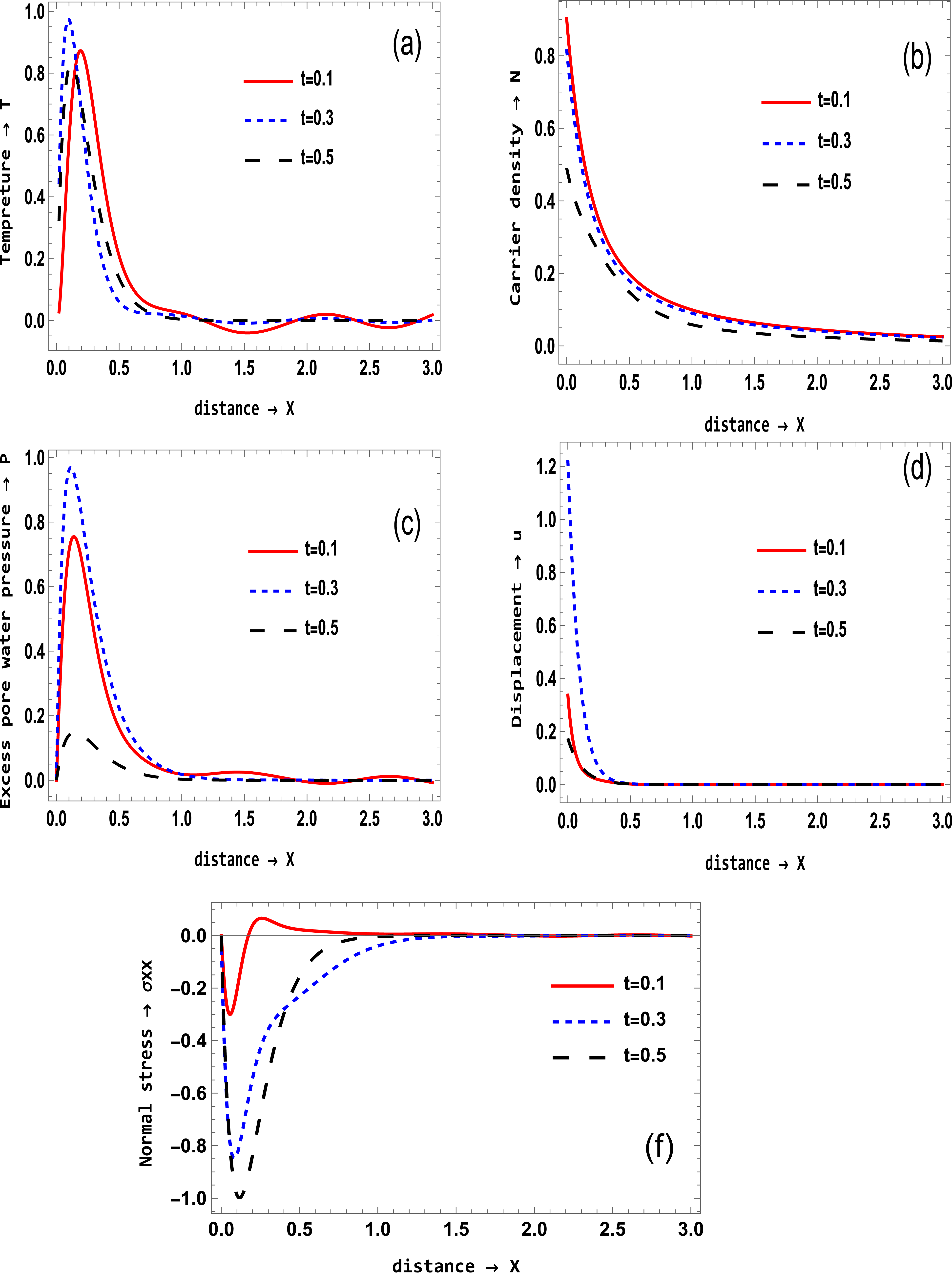
These deterministic results serve as a baseline to evaluate the effect of stochastic variations.
Stochastic behavior (Figure 2)
Figure 2 shows the influence of stochasticity introduced via white noise boundary conditions. Unlike the smooth deterministic profiles, the stochastic fields display sample-path variations due to random thermal and carrier fluctuations. • Temperature distributions fluctuate around the deterministic mean, with pronounced irregularities near the excitation surface. These arise from random thermal energy deposition due to fluctuating laser input or environmental instability. • Carrier density exhibits stronger fluctuations, reflecting stochastic transport and recombination of charge carriers under variable thermal fields. • Pore water pressure, inherently linked to thermal expansion, also fluctuates significantly near the boundary, indicating sensitivity to random excitation. • Displacement and stress become spatially non-uniform, with mechanical responses deviating due to the cumulative effect of thermal and pore pressure randomness. The stochastic of the dimensionless variables with the stochastic case with
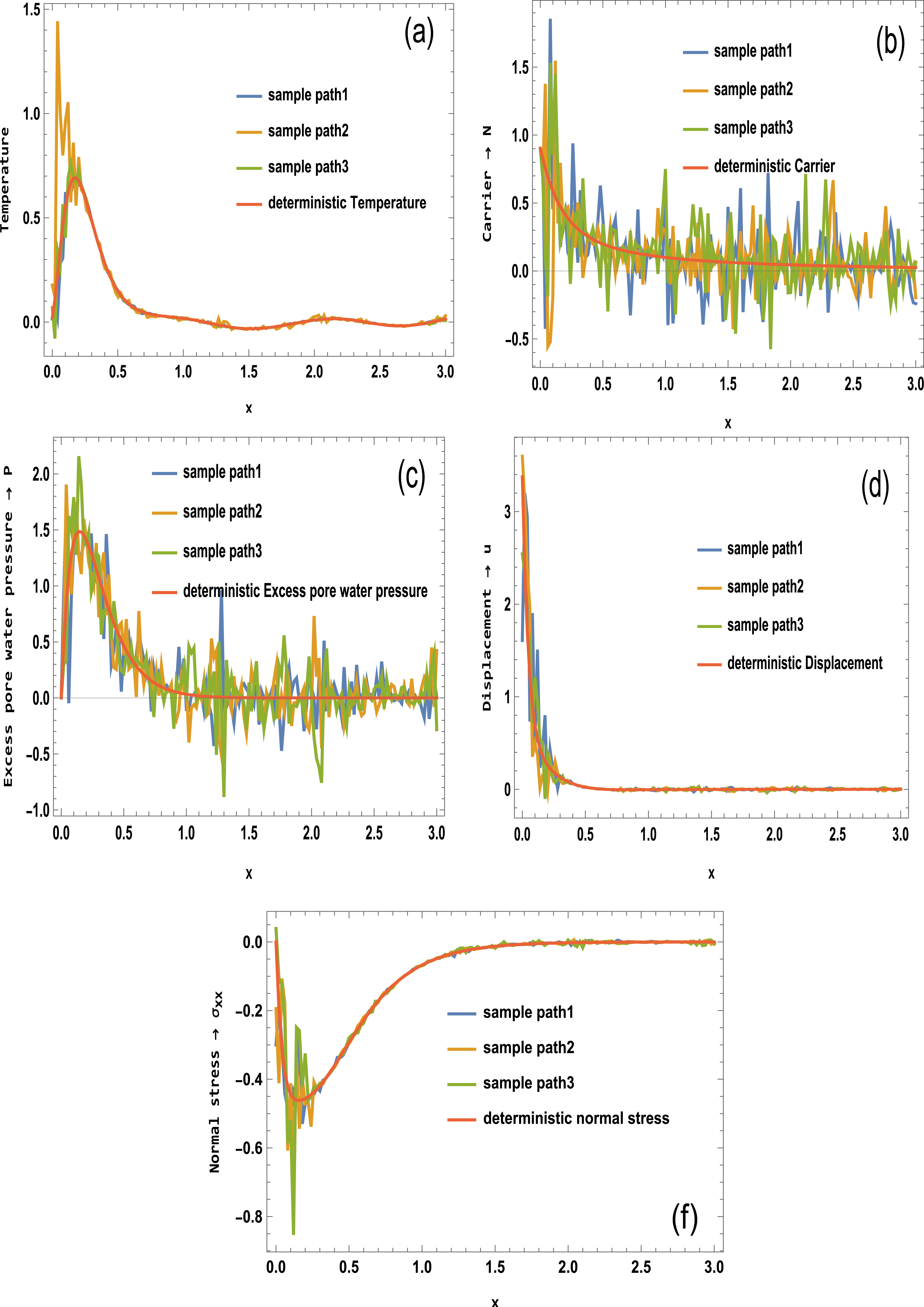
These results highlight the role of randomness in destabilizing wavefronts and shifting energy propagation pathways.
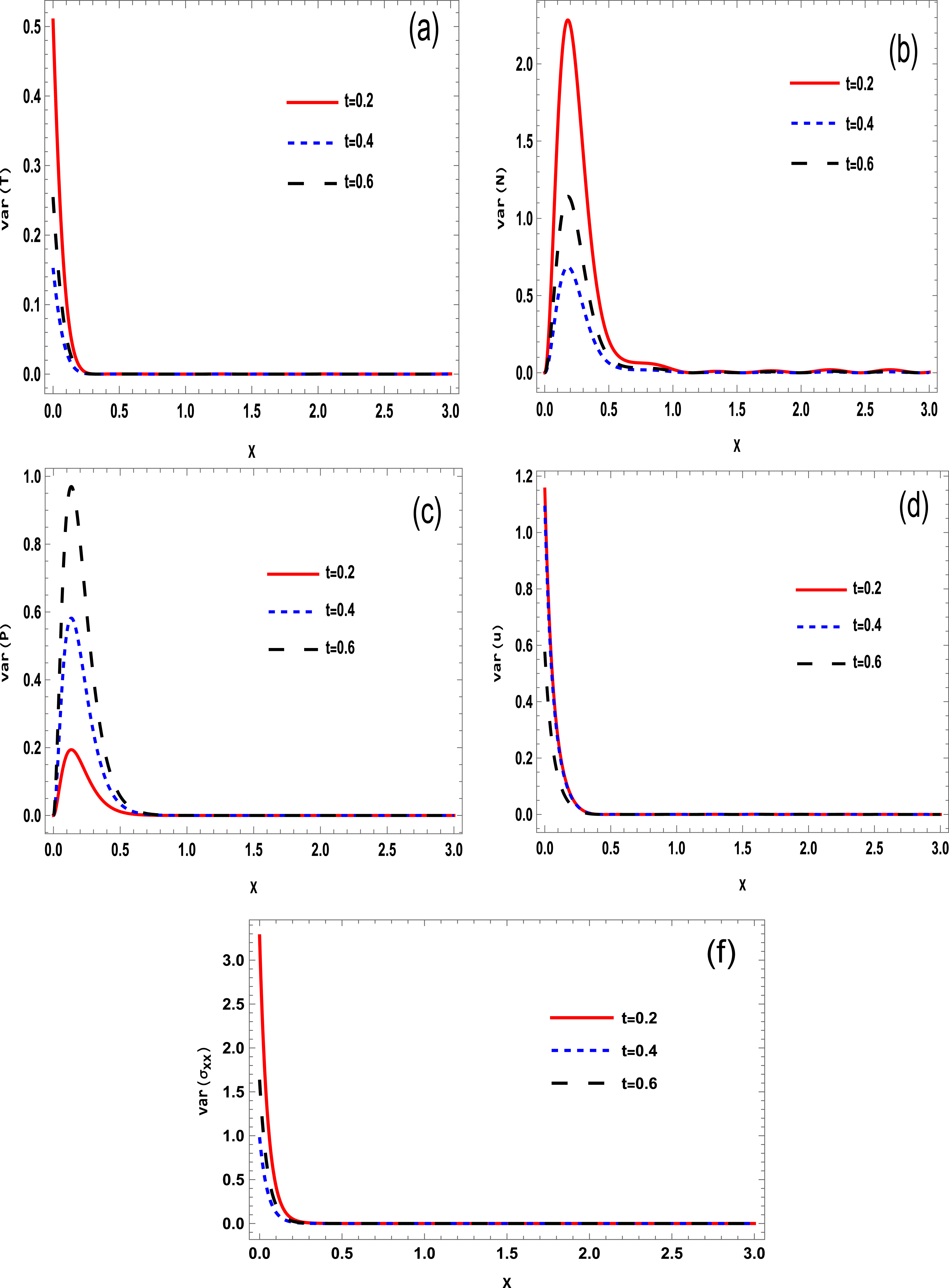
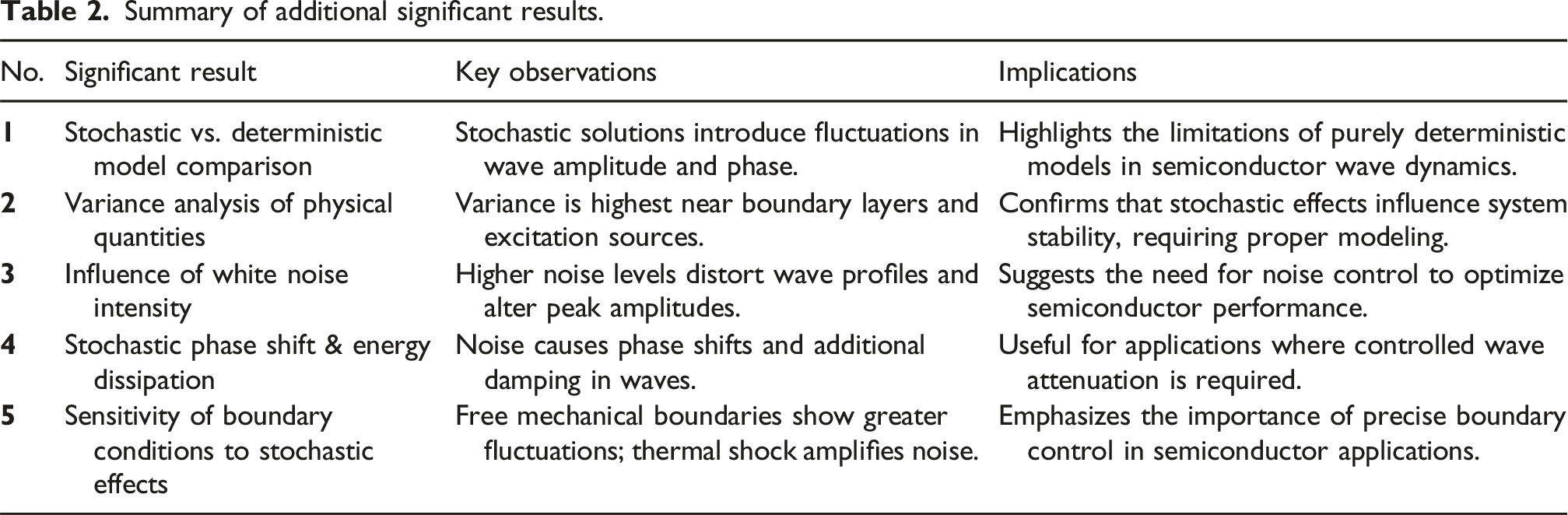
Variance analysis (Figure 3)
Figure 3 presents the spatial variance of the stochastic fields, providing a statistical measure of fluctuation intensity. • Temperature, displacement, and stress variances are highest near the boundary and decay exponentially with distance, indicating that stochastic disturbances are most pronounced at the excitation interface and dissipate as waves travel deeper into the material. • Carrier density and pore pressure variances display a distinct pattern: zero at the boundary, peaking at intermediate depths, and then decaying. This suggests a resonant region where coupling between thermal, electronic, and fluid fields amplifies instability before stabilization occurs. The (dispersion) of the dimensionless variables about its mean against the x distance.
Mechanistic Insight:
The overall behavior can be interpreted as follows: • A thermal shock initiates heat conduction and elastic wave propagation. • Heat induces electron excitation and pore fluid expansion, triggering carrier transport and pore pressure waves. • When randomness (white noise) is introduced at boundaries (e.g., random laser intensity, temperature pulses), it perturbs wave • These stochastic perturbations accumulate and modify phase velocity, amplitude, and energy dissipation rates, especially where multi-physical coupling is strongest.
Such mechanisms reflect real-world conditions where thermal and electronic noise affect semiconductor reliability, particularly in nano-scale and porous materials. Significance of Stochastic Analysis in Semiconductor Physics, the introduction of white noise fluctuations provides a more realistic representation of semiconductor behavior under laser excitation. Stochastic modeling helps in understanding unpredictable variations in semiconductor materials, which is critical for designing robust semiconductor devices that operate under thermal and electrical noise conditions. The comparison between deterministic (Figure 1) and stochastic (Figure 2) models emphasizes that real-world semiconductor interactions are inherently uncertain, requiring stochastic mathematical frameworks for accurate predictions.
Significance of White Noise in Variance Analysis: The presence of stochastic white noise in the system results in non-uniform fluctuations, making wave behavior less predictable and introducing uncertainty in semiconductor performance. The variance patterns suggest that stochastic effects are more pronounced near boundaries and critical transition regions, which is crucial for designing semiconductor-based sensors, MEMS, and optoelectronic devices. Implications for Semiconductor Device Design: Understanding variance trends helps in assessing the reliability and stability of semiconductor materials under photothermal excitation. Regions with high variance indicate where semiconductor performance might be more unpredictable, which is crucial for improving device precision and thermal management strategies.
To reflect the accuracy of our stochastic simulation, we performed an error analysis based on the statistical variance of each physical quantity. For each point along the spatial domain, the variance computed from multiple sample paths was used to calculate the standard deviation, representing the range of possible fluctuations around the mean. These error bars highlight regions where the stochastic response is more uncertain, typically near the thermal excitation boundary, while confirming greater stability in regions deeper within the material. This statistical representation reinforces the reliability of the model predictions and quantifies the effect of randomness on wave propagation behavior.
Since this is a numerical simulation study, no physical measurement equipment was used. However, to mimic experimental uncertainty, we consider computational sources of error such as numerical inversion of Laplace and Fourier transforms, finite discretization of space-time domains, and truncation effects. These sources are minimized by using validated numerical schemes and sufficiently dense computational grids. Additionally, convergence tests were performed to ensure result stability.
This dual approach, statistical variance from stochastic processes and numerical precision analysis, ensures that the reported results accurately reflect both physical randomness and computational reliability, enabling robust interpretation of stochastic wave behavior in semiconductor media.
Summary of additional significant results.
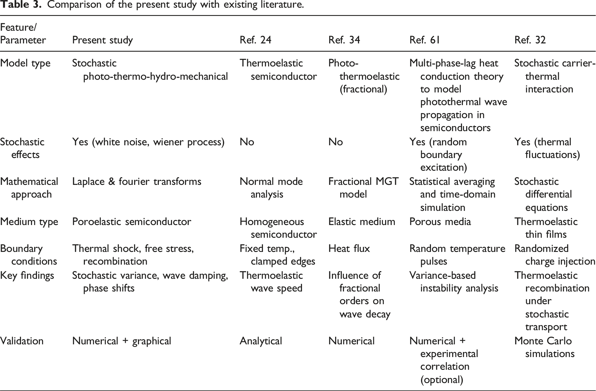
Comparison of the present study with existing literature.
The deviations observed between our stochastic results and classical deterministic models are primarily attributed to the inclusion of white noise perturbations in the boundary and governing equations. Unlike prior studies that assume smooth and deterministic wavefronts, our model reveals fluctuations in the amplitude and variance of temperature, stress, and carrier density fields. These deviations are particularly significant near excitation surfaces, where thermal gradients are highest.
Although experimental validation is beyond the current scope, the model’s predictions are compatible with experimental observations reported in previous photothermal studies using laser-based diagnostics. We propose that future experimental work using laser-induced photoacoustic techniques, infrared thermography, or micro-Raman thermometry in porous silicon or similar semiconductor structures could validate the stochastic wave patterns and variance profiles predicted here.
On the other hand, the physical validity of our theoretical model is further supported by experimental studies available in the literature. Kreuzer 5 demonstrated the effectiveness of photoacoustic spectroscopy in detecting thermal wave propagation resulting from infrared laser excitation, which aligns with our model’s treatment of thermal shock-induced wave generation in semiconductor media. Additionally, Todorović et al. 9 provided experimental evidence for both thermoelastic and electronic deformation mechanisms in semiconductors using frequency-based photoacoustic techniques. Their findings support the dual nature of wave generation considered in our model, where carrier excitation and thermal expansion jointly contribute to wave propagation. These experimental observations affirm the real-world applicability of our stochastic photo-thermoelastic framework and validate the coupling between thermal, mechanical, and electronic fields under stochastic excitation.
Conclusion
This study presents a novel stochastic photo-thermo-hydro-mechanical model for poroelastic semiconductor wave propagation that incorporates the effects of white noise fluctuations. By extending the generalized photo-thermoelasticity theory to include hydromechanical coupling and stochastic boundary conditions, the model offers a realistic framework for analyzing semiconductor behavior under thermal and mechanical uncertainties. Analytical solutions were obtained using Laplace and Fourier transforms, and numerical simulations were used to compare deterministic and stochastic behaviors.
The following key findings and contributions summarize the main outcomes of the study: • Stochastic modeling was introduced in photo-thermo-hydro-mechanical wave propagation in poro-semiconductors using white noise and Wiener processes. • Variance analysis was performed to evaluate the impact of randomness on temperature, carrier density, displacement, stress, and excess pore water pressure. • Stochastic boundary conditions, such as thermal shock and carrier recombination, were included to simulate realistic physical processes. • The variance of temperature, displacement, and stress exhibited exponential decay with distance, indicating energy dissipation and wave attenuation due to stochastic perturbations. • In contrast, carrier density and water pressure variances showed peak values at intermediate depths, revealing zones of maximum instability within the semiconductor medium. • Comparisons between deterministic and stochastic results showed that randomness alters wave amplitudes, introduces phase shifts, and affects the stability of the wavefront. • The model demonstrates practical relevance for designing advanced semiconductor devices such as MEMS, nanoelectronic sensors, and optoelectronic systems by accounting for inherent uncertainties. • The work provides a new analytical toolset for future studies involving stochastic effects in wave propagation, especially in porous and complex media.
Key findings and contributions
These findings confirm that incorporating stochastic analysis is essential for accurately modeling semiconductor wave dynamics and improving device performance under realistic operational conditions. (1) Realistic Modeling: o The incorporation of stochastic white noise effects provides a more accurate representation of real-world semiconductor wave behavior. o This accounts for fluctuations in material properties, boundary conditions, and external excitation sources. (2) Hydromechanical and Photothermal Coupling: o The interaction between fluid saturation, thermal waves, and charge carriers significantly influences semiconductor material response. o The study highlights how hydrostatic stress and photothermal excitation impact wave propagation and energy dissipation. (3) Statistical Predictability and Device Reliability: o Variance analysis confirms that stochastic perturbations are most pronounced at boundaries and transition regions, where wave interactions are strongest. o Understanding these variations is critical for designing robust semiconductor devices, including MEMS, optoelectronics, and laser-driven material systems. (4) Applications in Modern Engineering and Physics: • The findings can be used to optimize the design of semiconductor materials where random thermal and electronic fluctuations must be accounted for. • The results confirm that stochastic analysis is crucial for accurately predicting wave behavior in complex semiconductor structures. • Future research can extend this work by incorporating nonlinear effects, quantum-scale fluctuations, and material heterogeneity to further refine the model. • The integration of stochastic modeling with semiconductor device design can lead to enhanced stability, efficiency, and performance in next-generation electronic and photonic technologies.
Future recommendations and prospects
The study presented here highlights the complex interactions between photo-thermoelastic waves and hydrodynamic semiconductor media. Several prospects emerge for future research: (1) Advanced Material Modeling: Future studies could explore the development of more complex models for porous semiconductor metamaterials that account for various types of porosity, including micro-porosity and hierarchical porosity, and their influence on wave propagation and thermal conductivity. (2) Nonlocal Effects in Multiphysics Environments: The incorporation of nonlocal effects and their interaction with thermal, electromagnetic, and mechanical fields remains a promising avenue. Extending this work to more complex multiphysics problems involving electro-thermal-fluid coupling could yield valuable insights into the behavior of nanostructured semiconductors under extreme conditions. (3) Nanostructured and Metamaterial Enhancements: With the rapid advancements in nanotechnology and semiconductor metamaterials, investigating the effects of scaling and quantum effects on wave propagation in fractional photo-thermoelasticity is crucial for potential applications in next-generation semiconductors and optoelectronics. (4) Cross-disciplinary Applications: Beyond semiconductor devices, the methodologies developed here could be applied to other materials such as polymers and composites, where photo-thermoelastic and nonlocal effects play a significant role in device performance, particularly in smart materials and sensors. (5) Optimization for Industrial Applications: The results of this study can be further extended to optimize the design of semiconductor devices, such as lasers, photodetectors, and solar cells, by fine-tuning the properties of materials to enhance their performance under dynamic thermal and mechanical loads.
Footnotes
Acknowledgments
The authors thank the Princess Nourah bint Abdulrahman University Researchers Supporting Project number (PNURSP2025R899), Princess Nourah bint Abdulrahman University, Riyadh, Saudi Arabia for supporting this study.
Author contributions
All authors have equally participated in the preparation of the manuscript during the implementation of ideas, findings results, and writing of the manuscript.
Funding
The authors disclosed receipt of the following financial support for the research, authorship, and/or publication of this article: This work was supported by Princess Nourah bint Abdulrahman University Researchers Supporting Project number (PNURSP2025R899), Princess Nourah bint Abdulrahman University, Riyadh, Saudi Arabia.
Declaration of conflicting interests
The authors declared no potential conflicts of interest with respect to the research, authorship, and/or publication of this article.
Data Availability Statement
Current submission does not contain the pool data of the manuscript but the data used in the manuscript will be provided on request.