
Abstract
In this study, silicon carbide (SiC) microfibers were added as reinforcement to improve the thermomechanical properties of poly (methyl methacrylate) polymer, PMMA, since this type of composite has not been explored well enough so far. The aim of this study is to obtain PMMA/SiC composite materials with superior mechanical and thermal qualities out of the starting material, which are customizable for potential applications in flexible electronics as protective/buildable films. Thin PMMA composite films with 0.5 wt.% and 1.0 wt.% SiC microfibers regarding PMMA were made by casting. The Differential Scanning Calorimetry (DSC) analysis verified that the PMMA/SiC composites achieved greater thermal stability than the neat PMMA due to the presence of SiC microfibers. The glass transition temperatures of PMMA/0.5 wt.% SiC and PMMA/1.0 wt.% SiC films were around 2.4°C and 3.5°C higher, respectively, in comparison with the pure PMMA film. The results also showed that the PMMA films with 0.5 wt.% and 1.0 wt.% SiC reinforcement had 17.9% and 55.6% improvement in microhardness, respectively, compared to the neat PMMA film. The Atomic Force Microscopy (AFM) characterization of the PMMA composite films was also carried out. The addition of SiC microfibers to the PMMA polymer matrix also caused an increase in the roughness of the PMMA/SiC films. The average roughness values of the PMMA/SiC films were approximately 3.9 (with 0.5 wt.% SiC) and 13.7 (with 1.0 wt.% SiC) times larger than those obtained for the pure PMMA film. AFM in semi-contact operation mode was used to obtain 3D images of Vickers indents on the surface of PMMA and PMMA/SiC composite films. Both optical and atomic force microscopy approved the presence of pile-up effect after the indentation of PMMA films.
Introduction
The matrix material used in this study is poly (methyl methacrylate) (PMMA). This transparent amorphous thermoplastic polymer has many great qualities, including low weight, high impact strength, colorlessness, clarity, and superior insulation, but it also has low utilization temperature and poor fatigue resistance.1,2 With a refractive index of 1.49, good chemical resistance, thermal stability, mechanical flexibility, low cost, PMMA is a significant thermoplastic polymer.3,4 Since PMMA is lightweight, shatterproof, optically clear (transparent), and has good manufacturing conditions, it is frequently utilized as an alternative to inorganic glass. Resistance to weather and scratches are two exceptional qualities. PMMA is a promising polymer with potential uses in conductive devices, optical, sensor, pneumatic actuation, and analytical separation. Biomedical applications, polymer electrolytes, polymer viscosity, and drug administration by electro-diffusion or electro-osmotic flow are some further uses for PMMA. Nanotechnology greatly benefits from the use of PMMA with carbon nanotubes or other inorganic materials, because of its compatibility and ease of processing as a polymer moiety.5–7 PMMA is widely recognized for its capacity to produce materials with excellent qualities at low cost, including mechanical resistance, electrical insulation, thermal stability, and transparency.8,9
In addition to electronics and micro-optics, PMMA is also very sought for application in microfluidic devices due to its biocompatibility. PMMA has various advantages over other transparent polymers (such as polycarbonate, polystyrene, etc.), including superior light transmission and strong resistance to UV rays and weathering. This colorless polymer can be found in sheets, granules, pellets, and powders.10,11
Thus, a variety of fillers can be added to polymer-based nanocomposites. One of the primary fillers for sophisticated high-power and high-temperature electronic applications is silicon carbide (SiC). In order to produce materials that require a low coefficient of thermal expansion and high thermal conduction characteristics, silicon carbide has pioneered the creation of structural ceramics with exceptional performance. 9 Certain characteristics of silicon carbide nanostructures make them advantageous for usage in optoelectronics and microelectronics. In reality, SiC has been chosen because of its qualities, such as its high hardness and use in semiconductor processing equipment. SiC is an ideal candidate for high-power electronic devices because of these properties.12–14 One of the most popular materials for wear applications is silicon carbide. In order to enhance the mechanical, wear, or thermal properties of epoxy matrices, nanosized SiC particles - typically up to 3% by weight - have been incorporated.15,16
The incorporation of untreated and silane-treated SiC nanoparticles into the PMMA matrix improved the thermal stability, Young’s modulus and hardness of the PMMA nanocomposites. Better thermomechanical properties were achieved by the surface modified SiC nanoparticles.9,17 The simultaneous addition of SiC and TiO2 nanoparticles to the PMMA dental base material enhanced its tribological and mechanical properties by upgrading its modulus of elasticity and hardness, and reducing its wear rate and coefficient of friction. 18
The PMMA/PEG/SiO2/SiC nanostructures and their dielectric characteristics are suitable for a wide range of nanoelectronics’ applications thanks to their low-cost, minimal energy loss and high-energy storage capacity. Compared to alternative sensors, these nanostructures showed exceptional flexibility, durability in the environment, and strong pressure sensitivity. An investigation has already begun into the nanostructures for pressure sensing.19,20
After reviewing the literature, it has been found out that PMMA is a very popular material, but not enough research of SiC fibers as reinforcement in a PMMA matrix has been carried out. Silicon carbide has been added into PMMA mainly in the form of nanoparticles, but fiber forms are extremely rare. In the thin film technology, the choice of these materials opens up a range of possible applications in modern electronics for flexible devices. The aim of this study is to transform the initial material into a composite material with improved mechanical and thermal properties by adding long and thin SiC microfibers into the neat PMMA matrix. The modified properties of PMMA/SiC composite can be used in numerous optical and nanoelectronics applications.21,22
The purpose of this study is to examine the effects of adding SiC microfibers, as reinforcement, into the PMMA polymer, with different concentrations (0.5 wt.% and 1 wt.%). The thermomechanical properties and topography of the films were studied. Furthermore, the different indentation effects on the indent recovery of PMMA and PMMA/SiC composite films have been considered. In this research, the morphology and Vickers indent of PMMA based films were recorded by optical microscopy and Atomic Force Microscopy (AFM). Based on the size and shape of Vickers indent obtained after unloading, viscoelastic recovery of the indentation of PMMA films have been discussed.
From the aspect of material characterization of thin hybrid films, the profile (shape and depth) of the indent was studied after the Vickers test, by using the AFM technique. The influence of the SiC microfibers in the PMMA matrix on the shape of profile after unloading the indenter is of great interest for the elastic-plastic response of the tested material, and potential application and fabrication of MEMS (micro-electromechanical system) devices used as sensors for measuring low pressure.
Experimental part
Materials
Heat-resistant PMMA pellets, Acryrex CM-205 (Mw = 90400, Chi Mei Corporation, Taiwan), were the polymer components of the composite dissolved in acetone (MeiLab, Serbia). As reinforcement, the SiC nanofibers (D <2.5 μm, L/D ≥20, metal basis 98%, Sigma Aldrich) were added into the PMMA matrix.
Method-Preparation of the films
In order to produce the PMMA films, the pure PMMA pellets were dissolved in acetone and the SiC microfibers were added in different concentrations of 0.5 wt.% and 1.0 wt.% regarding PMMA. The final solution was stirred for 24h. The PMMA films were produced using the solution casting method by pouring the solutions into the Petri dishes and kept them to dry at room temperature in order to remove the residual solvent.1,11,23 The produced films were around 200 μm thick and their thickness was measured by the mechanical comparator (NP37, Iskra).
Characterization
A Nicolet 6700 spectrometer (Thermo Scientific) was used to perform the FTIR spectroscopy at 4 cm-1 in the attenuated total reflection mode. The wavelength range in which the spectra were captured was 4000 - 400 cm-1.
The morphological analysis of PMMA composite films, which were coated with Au, was performed by the field emission scanning electron microscopy (FE-SEM) on the Tescan Mira3 XMU electron microscope. EDS analysis was carried out using an INCAx-act LN2-free analytical silicon drift detector of characteristic X-rays that was paired to the electron microscope at 20 kV and used the PentaFET® Precision and Aztec 4.3 software package (Oxford Instruments, UK).
XRD experiments were performed using Proto AXRD Benchtop Powder X-ray Diffractometer with a copper X-ray tube. The generator was run at 30 kV and 20 mA. Thin film PMMA/1 wt.% SiC was scanned at diffraction angle 2θ from 30° to 90° at a scan rate of 0.86°/min to explore its crystalline structure.
The thermal properties of the PMMA composite films were examined in the nitrogen atmosphere heated with a continuous nitrogen flow of 50 mL/min, from 30°C to 130°C, at a heating rate of 10°C/min using a differential scanning calorimeter (DSC, Shimadzu – DSC-60 Plus).
The Vickers Hardness Number (VHN), also known as the indentation hardness, was determined using the formula VHN = 1.855P/d2, in which d (mm) is the length of the mean indentation diagonal and P (kilogram-force or kilopound) is the applied load.24–26 Three indents were made for each film using a micro-Vickers hardness tester (Leitz Kleinert Prufer DURIMET I), and the applied indentation load was 50 pounds (0.49 N) for 25 s. The optical microscope (Olympus CX41) created images of the indents, which were then used in the Image-Pro Plus software to measure the diagonal lengths of the indents. The equation used to determine hardness includes the average indentation diagonal length of a particular film.
The Atomic Force Microscopy (AFM) characterization of PMMA matrix and PMMA composite films (PMMA/0.5 wt. % SiC and PMMA/1.0 wt. % SiC) was performed using the ‘NTEGRA AFM’ device (type: NT-MTD Moscow, Russia). The software used for the AFM measurements was ‘NovaS, Image Analysis 2.2.0 NT-MDT’ and the measurements were conducted using the semi-contact mode with a cantilever resonant frequency of 150 kHz. 27 The NSG01 cantilever was used (made of n-type single crystal silicon (0.01-0.25 Ω⸱cm)). It had been doped with antimony and covered in an Au reflecting coating. The scan size area was 20 × 20 µm2 for the PMMA-based films, and 90 × 90 µm2 for the Vickers indents on the films surface. The quantitative roughness parameters were calculated using free software WsXM 4.0, version Beta 9.3. 28 All measurements were conducted with 256 points per line and 256 lines in total.
Results and discussion
SEM and EDS analysis
The appropriate SEM images and the EDS elemental mappings of the PMMA composite films are depicted in Figures 1 and 2 (scale bar 50 μm). The white traces of the SiC microfibers in Figure 1(a) confirm their good dispersion. In both images (Figures 1(b) and 2(b)), it is evident that the major element is C (green color), which comes from the PMMA resin and the SiC microfibers, besides the PMMA-related O element (red dots) and Si element (blue dots). The weight contents of the elements were: C - 69.91 wt.%, O - 29.91 wt.%, Si - 0.18 wt.%. The Si elemental mapping (Figure 1(c)) verified that the SiC microfibers (blue spots) were well dispersed and did not form any big clusters in the PMMA/0.5 wt.% SiC film, improving its thermomechanical performance. PMMA/0.5 wt.% SiC film: (a) SEM image; EDS elemental mapping of (b) all elements and (c) Si element. PMMA/1.0 wt.% SiC film: (a) SEM image; EDS elemental mapping of (b) all elements and (c) Si element.
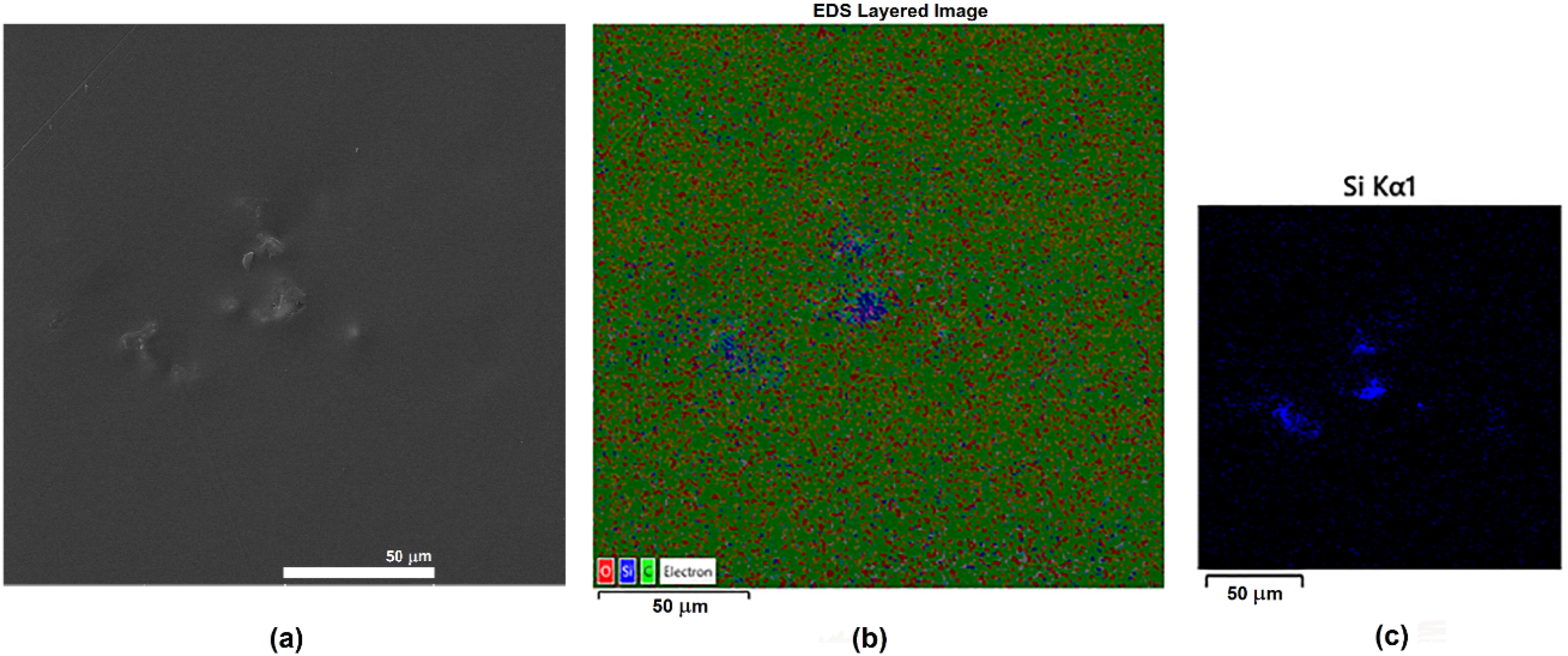
The white bundles in Figure 2(a) present SiC aggregates in the PMMA/1.0 wt.% SiC film, where their good SiC dispersion has not been achieved due to their higher concentration. These SiC agglomerates are obviously visible in Figure 2(b) and 2(c). However, this fact did not endanger the enhanced thermomechanical properties of the PMMA film with 1.0 wt.% SiC microfibers. The weight percentages of the elements were: C - 70.79 wt.%, O - 28.96 wt.% and Si - 0.25 wt.%.
XRD analysis
The SEM image of the SiC microfibers and their XRD measurements are depicted in Figure 3. The diffraction peaks may be identified to a cubic structure where the diffraction peaks match with reference values for β-SiC (JCPDS Card. No. 29-1129). The observed peaks at 35.6°, 41.3°, 60.0° and 71.7° can be indexed to (111), (200), (220) and (311) lattice planes of SiC crystal, respectively. The high purity of the cubic β-SiC phase is indicated by the high intensities of the diffraction peaks.29–31 SiC microfibers: (a) SEM image; (b) XRD pattern.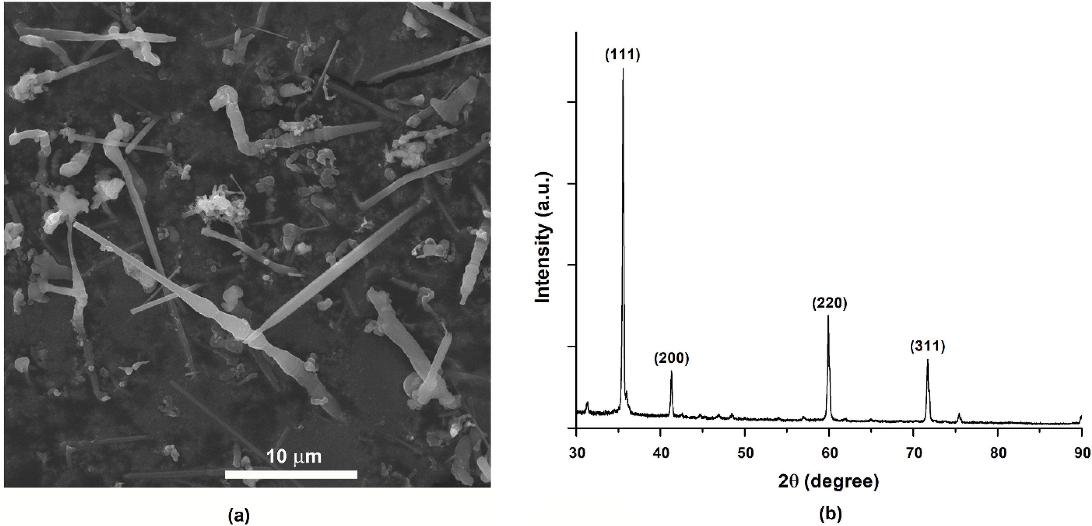
FTIR analysis
Figure 4 shows the FTIR spectra of different kinds of PMMA films and SiC microfibers. The bands at 780 cm-1 and 1051 cm-1 related to the Si–C and Si–O–Si stretching vibrations, respectively.32,33 Particular vibrations of PMMA were observed at 1720 cm-1 (C = O) and 1433 cm-1 (C–O). The bands at 2994 cm-1, 2948 cm-1 and 838 cm-1 corresponded to the C–H elongation of the CH3-metal groups. The peak at 1142 cm-1 represented the vibrations of ester group C–O, whilst the elongation ranges C–C are located at 985 cm-1 and 749 cm-1.9,34,35 FTIR analysis of SiC microfibers and different kinds of PMMA films.
The FTIR curves of PMMA and PMMA/SiC composites were almost of the same appearance because of the small amount of SiC fibers. According to the FTIR analysis, all the main PMMA bonds were present in the PMMA/SiC films. However, since the SiC fibers were included, which influenced the infrared absorption, the peak values were slightly different from those ones of pure PMMA. 36
DSC analysis
Differential scanning calorimetry (DSC) was used to examine the thermal properties of the films. The glass transition temperature (Tg) of the PMMA film was 73.5°C. There was a slight increase of Tg for the films with SiC microfibers. It was 2.4°C higher for the PMMA/0.5 wt.% SiC film (Tg = 75.9°C) and 3.5°C higher for the PMMA/1.0 wt.% SiC film (Tg = 77.0°C) compared to the neat PMMA film, Figure 5. DSC curves of different kinds of PMMA films.
The results of DSC analysis showed that the PMMA/SiC composites had a higher thermal stability compared to the neat PMMA, since the SiC microfibers decreased the overall mobility of the PMMA polymer chains as a result of their potential physical interactions with the polymer. It should be emphasized that the SiC fibers were chemically inactive towards the PMMA matrix, as it was confirmed by the FTIR analysis. Instead, their role in the PMMA-based composites is typical physical reinforcement through their dispersion, which improved mechanical and thermal properties of PMMA/SiC composites. In most cases, filler content usually increases Tg, reduces the polymer chain movement and gives stiffness to the composites.37–40
Microhardness analysis
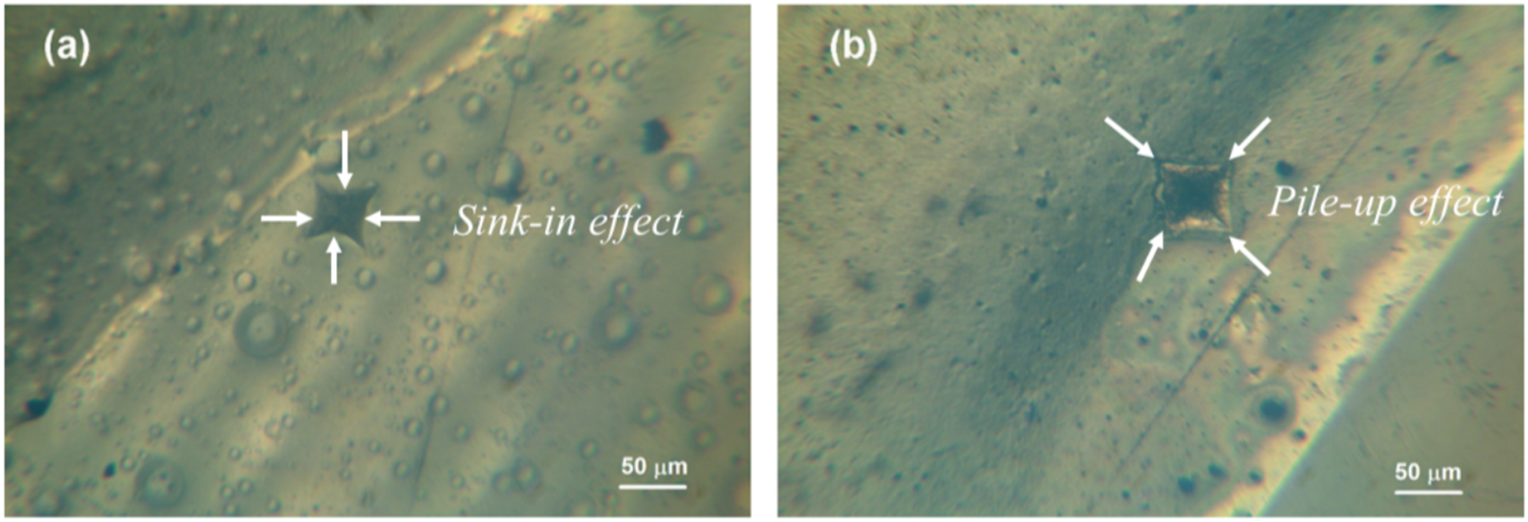
Micro Vickers indentation tests of the films showed that the addition of SiC microfibers raised their hardness value (Figure 6). The mean diagonal values were as follows: 68 ± 1.8 μm for the PMMA film, 63 ± 4.6 μm for the PMMA/0.5 wt.% SiC film and 55 ± 2.9 μm for the PMMA/1.0 wt.% SiC film. Due to its higher content of SiC microfibers, the PMMA/1.0 wt.% SiC film achieved the best hardness result. In comparison to the neat PMMA film, the results demonstrated that the PMMA films with the 0.5 wt.% and 1.0 wt.% SiC reinforcement improved their microhardness by 17.9% and 55.6%, respectively. Compared to the pure PMMA film (Figure 7(a)), the indent in the PMMA composite film (black area) is noticeably reduced (Figure 7(b)). The plastic deformation of the film around the indent is also visible in Figure 7(b). In fact, during the loading, the material under the indenter tip firstly undergoes an elastic regime that is followed by a plastic regime with plastic deformations. Usually, an elastic-plastic deformation occurs during the indentation loading of some polymer materials when their surface may depress (the sink-in effect) or rise (the pile-up effect) around the indenter.41–44 These effects are marked in Figure 7. Microhardness of all PMMA films. Optical images of PMMA films: (а) neat and (b) with 1.0 wt.% SiC microfibers.
AFM analysis
The AFM surface of PMMA and PMMA/SiC composite films and histograms of the topography of the films are shown in Figure 8. Figures 8(a), 8(c), and 8(e) represent 2D images, which were obtained with the same scanned area (20 × 20 μm2). Figures 8(b), 8(d), and 8(f) represent the corresponding distribution histograms obtained by analyzing 2D images. The surface topography of PMMA and PMMA/SiC composite films and their histograms of topography: (a) and (b) - PMMA matrix, (c) and (d) - PMMA/0.5 wt.% SiC, (e) and (f) - PMMA/1.0 wt. %. Scan size: (20 × 20) μm2.
The PMMA film (Figures 8(a) and 8(b)) had more uniform topography than films with the SiC microfibers (Figures 8(c)-8(f)). The topography (x-axis or height of spades) obtained for the PMMA film was about 100 nm (Figure 8(b)), while for the PMMA composite films it was in the range 150 nm for the PMMA film with the 0.5 wt.% SiC, and 900 nm for the film with the 1.0 wt.% SiC microfibers (Figure 8(d) and 8(f), respectively). The high values of height of spades for the PMMA/1.0 wt. % SiC film indicate large presence of the SiC agglomerates as it was confirmed by SEM image in Figure 2(а), and 2D surface topography in Figure 8(e).
The AFM analysis confirmed the difference between the films obtained from the neat PMMA film and the PMMA films with SiC microfibers by 3D images and their line profiles (Figure 9). Figure 9 shows the topography and the corresponding line section analysis of the neat film with no microfibers (Figure 9(a)), with the 0.5 wt. % of SiC (Figure 9(b)), and with the 1.0 wt. % SiC microfibers (Figure 9(c)). The line profile of the PMMA/1.0 wt. % SiC film (Figure 9(f)) was in coherence with its histogram in Figure 8(f). The 3D surface topography and line profiles of the films: (a) and (d) PMMA matrix, (b) and (e) PMMA/0.5 wt.% SiC, (c) and (f) PMMA/1.0 wt. % SiC. Scan size: (20 × 20) μm2.
Roughness parameters of PMMA composite films.

Ra is a useful metric for quality assurance, but it cannot distinguish between profiles with various forms. However, one of the most crucial factors for characterizing a rough surface is Rq, which is more sensitive to significant departures from the average line and is always larger than the average roughness Ra. The ability to compute confidence intervals and run statistical tests on regularly distributed data is one advantage of Rq over Ra. However, because Rq implies a heavy-tailed distribution, it is less appropriate than average roughness for monitoring surfaces with significant variations.
Based on the values given in Table 1, different roughness values were observed for the PMMA film and PMMA films reinforced with SiC microfibers. A drastic change in roughness parameters was observed with an addition of 1.0 wt.% of SiC microfibers in PMMA matrix, which also represents the film with the roughest surface. Both roughness parameters of this film (Ra = 268.2 nm and Rq = 334.5 nm) were about 3.5 times higher in comparison with the ones of the PMMA/0.5 wt. % SiC film. Compared to the values of the PMMA film, this Ra parameter of the PMMA/1.0 wt. % SiC film was about 13.7 times higher, while Rq value was around 11.3 times greater. Additionally, the surface of all films is slightly dominated by peaks, as indicated by the positive low values of Rsk. If Rku value is less than 3, it indicates that there are more valleys and fewer peaks on the surfaces (as in PMMA/1.0 wt. % SiC film). Surface roughness is a necessary consideration in the design of many devices that use supported polymer films. 46
An interesting study of the appearance of the Vickers imprint and the elastic displacement after indentation is presented for the matrix and the film with the higher reinforcement percentage (Figure 10). The diagonal size obtained from PMMA matrix according to Figure 10(c) was 69.39 μm, and the indentation depth was 2.33 μm. For the PMMA/1.0 wt. % SiC film, the diagonal size was 58.90 μm, while the indentation depth was 2.54 μm (Figure 10(f)). The AFM images of Vickers indents (2D, 3D, and profile) for the films: (a)-(c) PMMA and (d)-(f) PMMA/1.0 wt.% SiC. Scan size: (90 × 90) μm2.
AFM profile analyses seem to be a suitable tool for the shape and size evaluations of low-load indentation Vickers imprints, but with certain limitations - namely, the elastic response of polymer composites, 47 the aging time of recording the profile after indentation (retraction of the impression), 48 and the depth to which the profile can be recorded. 49 Elastic anisotropy and time-dependent viscoelastic recovery of PMMA coatings determined by AFM nanoindentation analysis are very suitable methods to predict the viscoelastic recovery of surface deformation for the viscoelastic materials such as PMMA. 50
The diagonal size obtained from PMMA matrix according to the optical microscopy was 68 ± 1.8 μm, and for the PMMA/1.0 wt. % SiC film it was 55 ± 2.9 μm. Deviations in the diagonal size for the PMMA film are insignificant when comparing the values from the optical microscope and AFM profile, however, the deviation for the reinforced composite (PMMA/1.0 wt. % SiC) was 7 %. This is probably because the indentation prints are performed near the edge of the SiC fibers on the surface of the PMMA composite, and the stress field in the PMMA created by the diamond indenter interacts with the much stiffer SiC fibers, resulting in an increase in the modulus value compared to the expected value for the neat PMMA. In the literature, this effect is known as ‘fiber-bias effect’. 51
It is also interesting to note that the penetration depth of the indenter deviates from the theoretical value of 1/7 the size of the diagonal 52 which is typical for metallic films. For an applied load of 0.49 N on PMMA based films, the indentation depth of a Vickers indenter is typically around 2 μm. This depth can vary slightly depending on the specific experimental conditions and the weight percent of fibers in the PMMA sample. Although the indenter penetration depth in harder PMMA composites is expected to be less than in a pure PMMA polymer matrix, this is not always the case in polymers reinforced with long fibers such as SiC. The type and orientation of fibers, the fiber volume fraction, and the mechanical properties of both the fibers and the PMMA matrix can together affect the pressure distribution during indentation. For example, better dispersion and alignment of fibers can lead to improved mechanical strength and more uniform pressure distribution. 53
The pile-up effect after micro indentation in PMMA film was observed in Figure 10 (a light field around the indent in Figure 10(a) and 10(b)), and a peak in the profile (Figure 10(c)). It is a phenomenon where PMMA is displaced around the indentation site, forming a pile-up around the indenter. This effect can influence the measurement of mechanical properties such as hardness and elastic modulus. The pile-up effect can lead to an overestimation of hardness because the actual contact area between the indenter and the material is reduced. 50
Investigation of the Indentation Size Effect (ISE) (the phenomenon where the hardness of a material varies with the size of the indentation and applied loads), and an indentation creep mechanism (oscillations of hardness values with application different indentation times) for PMMA/SiC composite after Vickers indentation tests will be investigated in the future research. However, the ISE effect observed in PMMA based materials cannot be explained by dislocation theory like in metals, but ISE mechanism in PMMA attributed to structural differences in depth of polymer, the elastic strain, stiffness of polymer chains, etc.. 54
Conclusion
In this study, the PMMA composite films were made by adding the SiC microfibers as reinforcement which may be applied in microelectronics. The improved thermomechanical properties of the films were confirmed by DSC analysis and Vickers indentation. In comparison with the PMMA film, the glass transition temperatures were 2.4°C and 3.5°C higher for the PMMA films with 0.5 wt.% and 1.0 wt.% SiC microfibers, respectively. The results also demonstrated that, compared to the neat PMMA film, the microhardness of the PMMA films with 0.5 wt.% and 1.0 wt.% SiC reinforcement had 17.9% and 55.6% improvement in microhardness, correspondingly. Following the indentation of PMMA films, the pile-up effect was confirmed by both optical and atomic force microscopy. The PMMA/1.0 wt. % SiC film had the roughest surface where the roughness parameters were about 3.5 times higher with their values compared to those ones of the PMMA/0.5 wt. % SiC film. Surface roughness needs to be taken into account while designing many devices that use supported polymer films.
Footnotes
Funding
The authors disclosed receipt of the following financial support for the research, authorship, and/or publication of this article: This work was financially supported by the Ministry of Science, Technological Development and Innovation of the Republic of Serbia (Contract Nos. 451-03-136/2025-03/200287, 451-03-136/2025-03/200026, 451-03-136/2025-03/200017).
Declaration of conflicting interests
The authors declared the following potential conflicts of interest with respect to the research, authorship, and/or publication of this article: The authors declare that the research was conducted in the absence of any commercial or financial relationships that could be construed as a potential conflict of interest.