
Abstract
First, chitin was reacted with 4,5-dichlorophthalic acid and diphenic acid, and thus two new chitin derivatives (C45DA and CDA) were synthesized. Then, C45DA and CDA were characterized by various spectroscopies and techniques (FTIR, 13C CP-MAS solid-state NMR, XRPD, SEM, and TGA/DTA). Besides, some electrical properties of C45DA were measured. After the characterization process, the Schottky diodes of C45DA and CDA were made. It was determined that these diodes showed photodiode characteristics at the same time. Later on, both electrical properties (ϕb , n, and Rs ) and photoelectrical properties (I Illumination/I Dark, I SC, and V OC) of these diodes were determined.
Introduction
Chitin is the most abundant biopolymer in the world after cellulose and is therefore very cheap. The fact that the chitin is a biopolymer and cheap makes it advantageous for use in different areas. Due to these reasons, chitin and its main derivative, chitosan that is obtained by deacetylation of the chitin, were widely used in many areas and systems for different purposes. Some of these areas and systems are adsorption, 1 –9 agriculture, 10 –14 artificial skin, 15 –17 burn treatment, 18 –20 chromatographic separation, 9,21 cosmetics, 15,22 diode construction, 23 –25 drug delivery systems, 26 –31 food processing, 32 –35 gene therapy, 36 –38 ophthalmology, 39,40 paper industry, 41 –46 solid state battery, 47,48 textile industry, 49,50 tissue engineering, 17,51 –55 wound healing/wound dressing, 50,56 –58 and so on. 59 –66 Very successful results were generally obtained in these studies and many other studies. Due to this reason, the studies that chitin and its derivatives are being used have been still continuing.
In our previous study, 25 novel chitin derivatives synthesized were characterized, and very important results were obtained related to the electrical conductivities of these derivatives. These derivatives were then used to make Schottky diodes, and the electrical properties of these diodes were found to be very good. It was also determined that the diodes constructed have photoelectrical properties. This study was performed with the thought that we can obtain better results than the results obtained in our previous study. 25
Experimental
Materials
2-Propanol, 4,5-dichlorophthalic acid, acetone, chitin (C9213), dichloromethane, diphenic acid, hydrogen chloride, hydrogen fluoride, n-type silicon wafer, powder gold, thionyl chloride, and trichloroethylene were purchased from Sigma-Aldrich Corp. (St. Louis, Missouri, USA). Lithium chloride, N, N-dimethylacetamide, tetrahydrofuran, and triethylamine were purchased from Merck Millipore Corp. (Germany).
Synthesis and characterization
About 150 mL of a tetrahydrofuran-dichloromethane (2:1) mixture at 60 °C was placed into a 250 mL three-necked flask. Then, 3 × 10⁻² mol 4,5-dichlorophthalic acid was added into this mixture, and the dissolution of 4,5-dichlorophthalic acid was provided. Besides, 0.6 mol SOCl2 was added dropwise into the flask via dropping funnel at room temperature and within 10 min, and the mixture was refluxed at 40 °C for 3 h after the entire SOCl2 was transferred into the flask. After reflux, tetrahydrofuran–dichloromethane mixture used as solvent and the remainder of thionyl chloride due to excessive use were removed via a rotary evaporator. The obtained product was dissolved in N, N-dimethylacetamide without purification and was reacted with chitin (Figure 1) as indicated in our previous study. 25 In the same way, the hydroxyl groups of diphenic acid were also converted to chlorides, and the obtained product, without dissolving in N, N-dimethylacetamide, was then reacted with chitin (Figure 2) as described in our previous study. 25 The resulting chitin derivatives were abbreviated as C45DA and CDA, respectively. The characterization of C45DA and CDA was performed as described in our previous study. 25
Scheme related to the synthesis of C45DA.

Scheme related to the synthesis of CDA.
Construction of Schottky diodes
The Schottky diodes constructed using the chitin derivatives synthesized in this study were constructed using the method and other materials (n-Si as semiconductor and Au as ohmic and rectifier contacts) stated in our previous study. 25 The scheme drawn for the Schottky diodes constructed is given as Figure 3.

Scheme of the Schottky diodes constructed.
Results and discussion
FTIR and 13C CP-MAS solid-state NMR analyzes
The characteristic absorption bands seen in Figure 4 and given in Table 1 confirmed that the chitin reacted with 4,5-dichlorophthalic acid and diphenic acid as shown in Figures 1 and 2. Besides, broad signal at 137.89 ppm related to the carbons of aromatic ring and signal at 170.66 ppm related to the carbons of ester carbonyls in Figure 5(a) and broad two signals at 133.87 and 145.82 ppm related to the carbons of aromatic rings in Figure 5(b) confirmed the reactions in Figures 1 and 2. The signal related to the carbons of ester carbonyls in CDA was not observed in Figure 5(b).

FTIR spectra of (a) C45DA and (b) CDA.
Some characteristic absorption bands in the FTIR spectra of C45DA and CDA.


13C CP-MAS solid-state NMR spectra of (a) C45DA and (b) CDA.
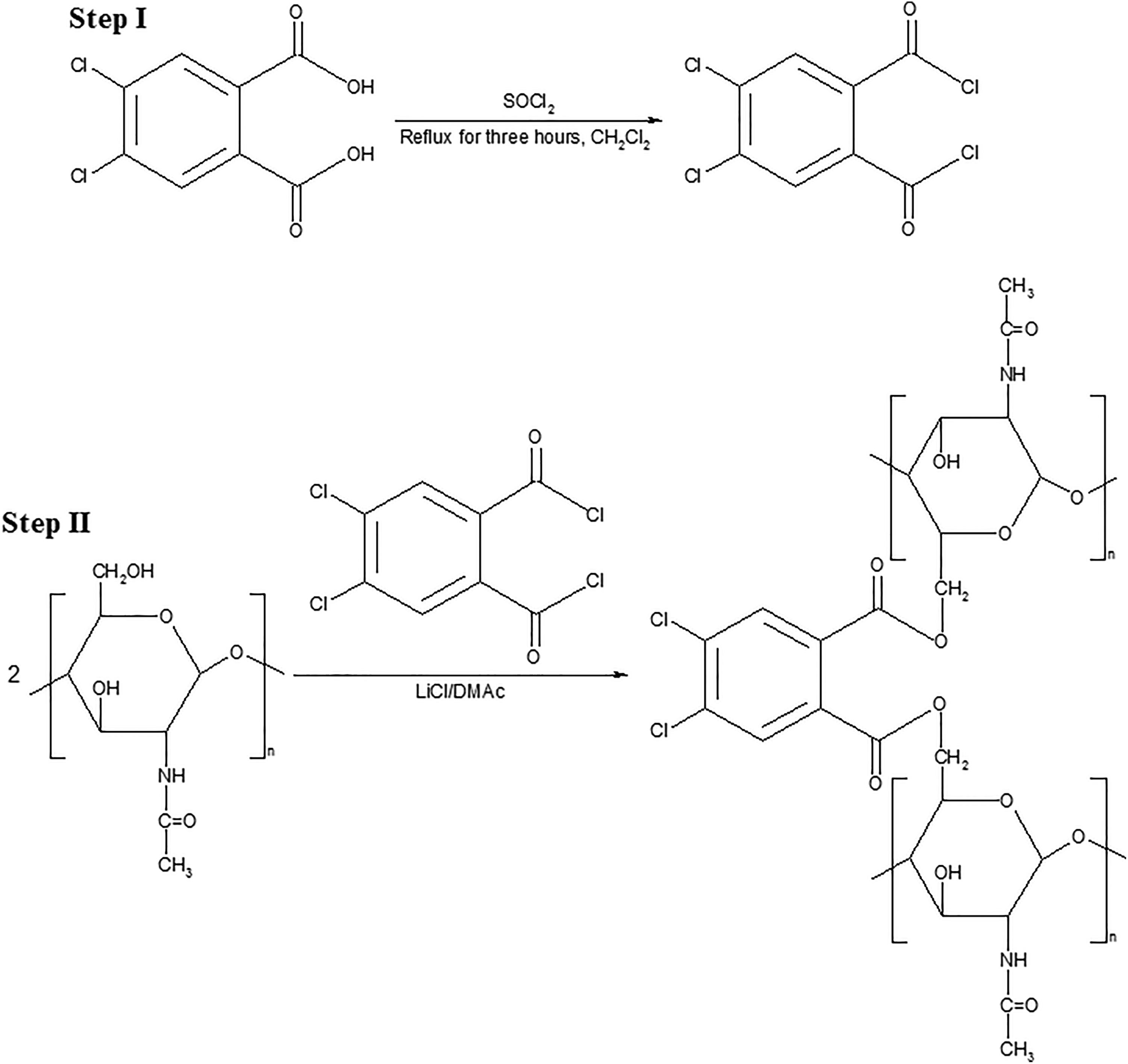
XRPD analysis
Some data obtained from the XRPD patterns of C35DA and CDA in Figure 6 and the

used in the synthesis was given in a previous study. 68 When the XRPD patterns of the chitin and C45DA are compared, it is seen that crystallizations related to the chitin in [002], [101], [130], and [063] planes disappeared. It is seen that the peaks related to the chitin in the other planes are smaller after the reaction. When the XRPD patterns of the chitin and CDA are compared, it is seen that crystallizations related to the chitin in [002] and [101] planes disappeared. In other planes outside [003] and [004] planes, and particularly in [063] plane, it is seen that the peaks related to the chitin are smaller after the reaction.
XRPD patterns of (a) C45DA and (b) CDA.
Some important information about the X-ray powder diffraction patterns of C45DA and CDA.

SEM analysis
Figure 7(a) shows that C45DA has a heterogeneous and rough surface as a whole. However, it can be said that it consists of much larger pieces than the chitin. In addition, homogeneous structure is also present in some narrow regions. Figure 7(b) shows that CDA has a heterogeneous and slightly rough surface as a whole. However, according to the chitin, it is seen that it is formed from pieces of different sizes and that it is a homogeneous structure in some very small regions.

SEM micrographs of (a) C45DA and (b) CDA.
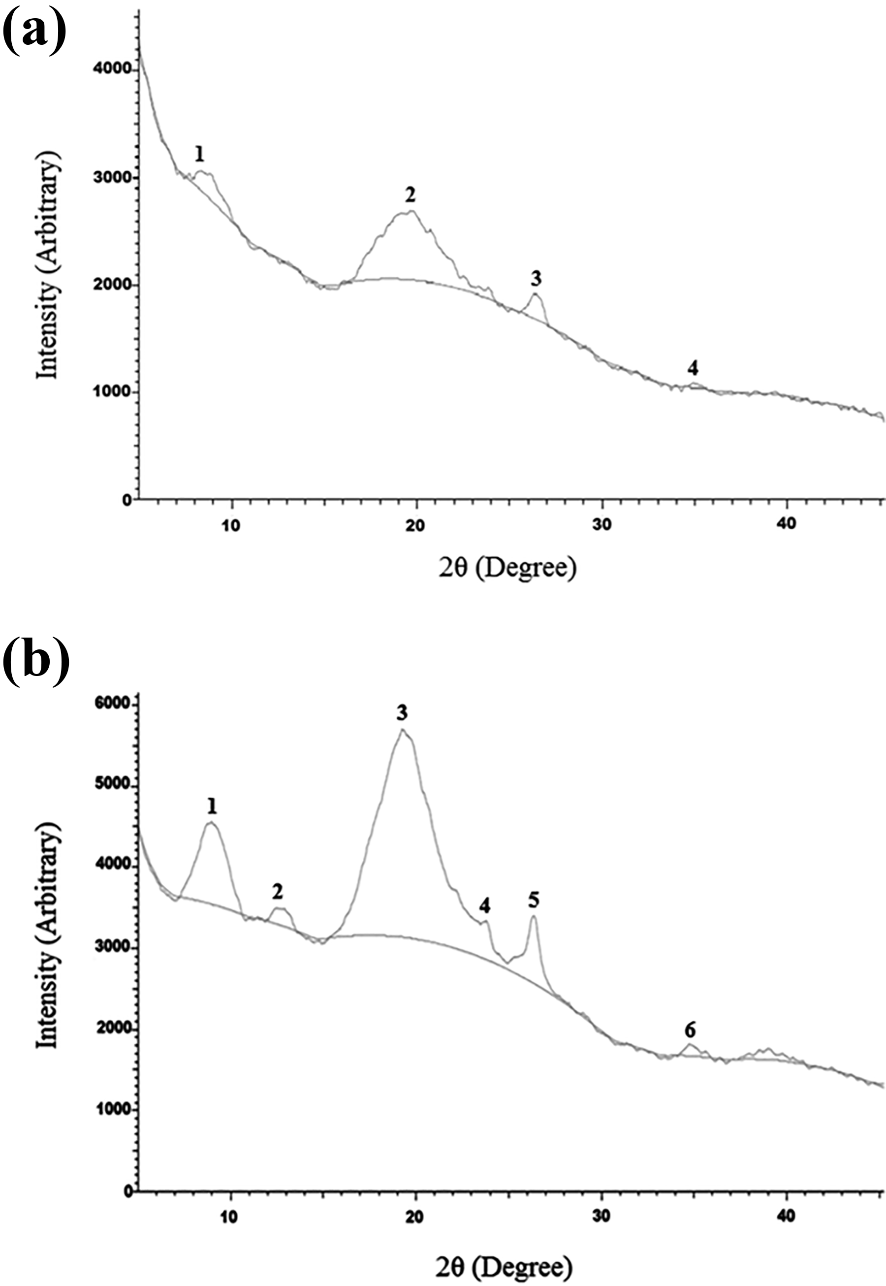
TGA analysis
The TGA curves of C45DA and CDA indicate that they have one decomposition stage, and the decomposition stage of both is in the range of about 205–345 °C (Figure 8). In some studies, 69 –71 it was stated that the polysaccharide structure of chitin was degraded in temperature ranges close to this temperature range. Besides, the TGA curves of C45DA and CDA indicate that they have almost the same thermal stability. The mass losses to approximately 100 °C of both C45DA and CDA are due to water evaporation in their structures.
TGA and DTA curves of (a) C45DA and (b) CDA.
Some electrical properties of C45DA
Charge carrier density, electrical conductivity, and hole mobility values of C45DA were determined as 2.580 × 1016 cm−3, 9.76 × 10⁻³ S cm−1, and 2.361 cm2 V−1 s−1, respectively. These electrical properties could not be determined for CDA due to its solubility problem. The semiconductivity range for materials is given as 10−7–10−1 S cm−1, 10−6–102 S cm−1, 10−5–100 S cm−1, 10−6–100 S cm−1, and 10−7–100 S cm−1 in some studies, 72 –76 respectively. As seen, we can say that C45DA is a good semiconductor even though the semiconductivity range is given differently in different sources.
Some electrical and photoelectrical properties of the Schottky diodes
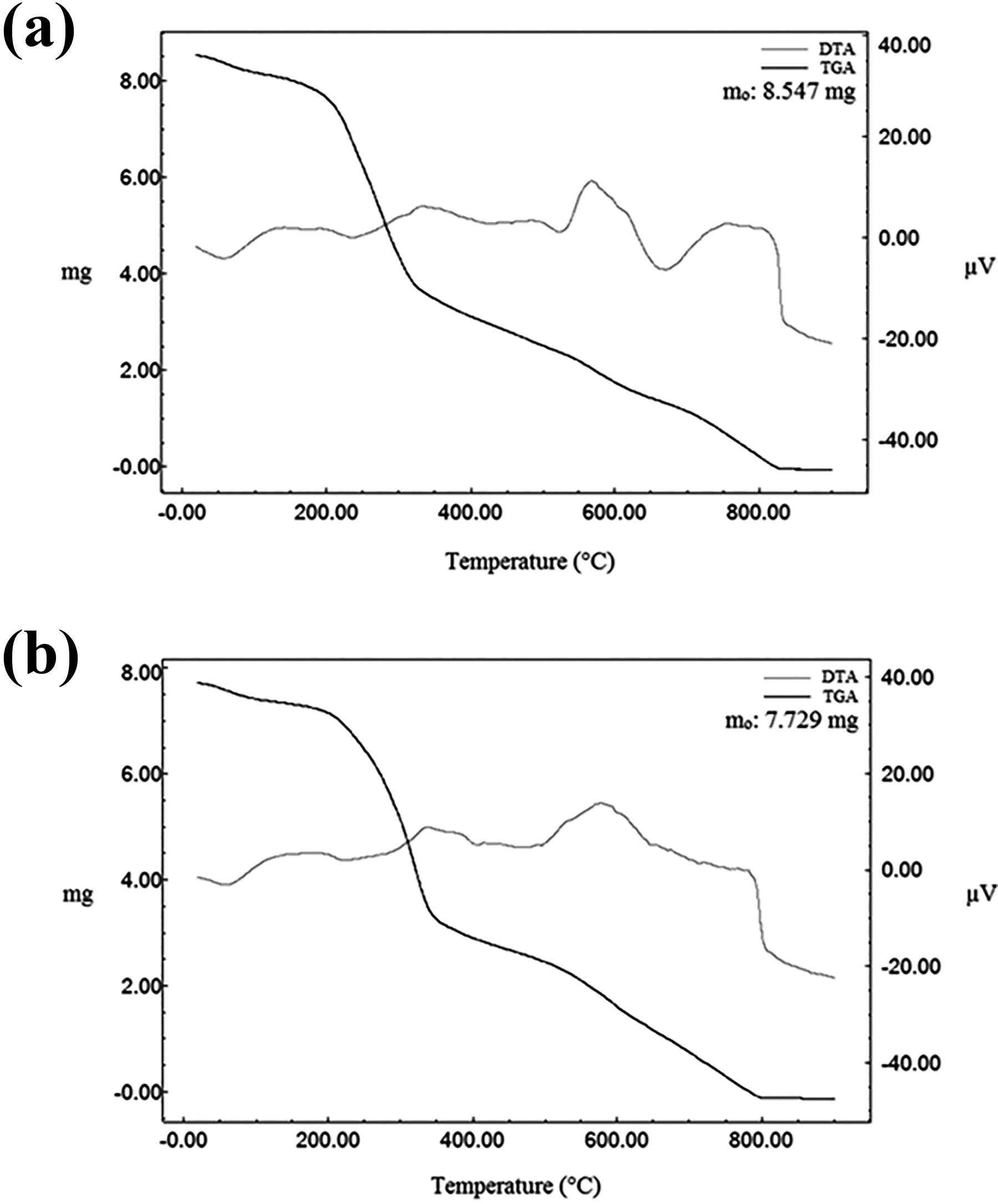
The I–V curves of Au/C45DA/n-Si/Au and Au/CDA/n-Si/Au structures are given in Figure 9. These structures can also be called diode, because they show the characteristic of the Schottky diode, which is a rectifying metal–semiconductor junction. The rectifying junctions show an exponential current increase in forward direction as a function of applied voltage, whereas they do not show a significant current increase in reverse direction. According to this, Au/C45DA/n-Si/Au and Au/CDA/n-Si/Au structures can be used as alternative diodes in clamping circuits, in clipping circuits, in logic gates, in reverse current protection, in solar panels, in voltage multiplier circuits, and in voltage spike suppression. Equation (2) is used to calculate the electrical properties of a diode.
77
The term


changing the organic interlayer. It is known that the ideality factor for an ideal diode is 1, and the ideality factor is calculated using the slope of the linear section of
Current–voltage curves of (a) Au/C45DA/n-Si/Au and (b) Au/CDA/n-Si/Au diodes.
Electrical and photoelectrical properties of Au/C45DA/n-Si/Au and Au/CDA/n-Si/Au diodes.
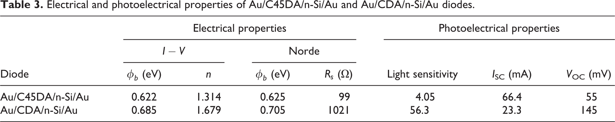
The barrier height of a diode can be calculated using the modified Norde function too. The Norde function and the modified Norde function are given as equations (5) and 6, respectively. Figure 10 shows the plot of F(V) versus V. The barrier heights of the diodes were also calculated using equation (7) from Figure 10. The deviations from linearity of the current curves in forward direction in Figure 9 show that the diodes have a series resistance. There are


many methods for calculating the series resistance of a diode, 78 –80 and for this aim the method in which the modified Norde function is used was used in this study. The series resistances of the diodes were calculated using equation (8) from Figure 10. The ϕb and Rs values calculated using the modified Norde function for the Schottky diodes constructed are given in Table 3. It

is seen from Table 3 that the

Norde function-voltage plots of Au/C45DA/n-Si/Au and Au/CDA/n-Si/Au diodes.
Both diodes exhibit light sensitivity because the current under illumination (a light density of 100 mW/cm2) according to the current in the dark is higher in reverse direction (Figure 9). That is, the diodes have photodiode property. According to this, Au/C45DA/n-Si/Au and Au/CDA/n-Si/Au structures can be used as alternative photodiodes in automotive devices, bar code scanners, cameras, medical devices, optical communication devices, position sensors, safety equipment, and surveying instruments. The fact that the current under illumination is larger than the current in the dark indicates that a photo-current was generated in these structures. This photo-current generated in the structures was attributed to the electron-hole pairs formed in the organic–inorganic interface in some studies. 81 –83 Some photoelectrical properties of Au/C45DA/n-Si/Au and Au/CDA/n-Si/Au diodes are given in Table 3. From Table 3, it can be seen that the light sensitivity of Au/CDA/n-Si/Au diode is much higher than that of Au/C45DA/n-Si/Au diode. Furthermore, it was determined that the light sensitivity of Au/CDA/n-Si/Au diode is higher than those of Au/C4NC/n-Si/Au and Au/C35DC/n-Si/Au diodes made in our previous study. 25 The light sensitivity of the diodes constructed was calculated by dividing the current under illumination to the current in the dark when a voltage of −2 V was applied.
Conclusions
Based on the experimental results obtained, the followings can be said: From the CrI values calculated, it was determined that CDA is more crystalline than C45DA. C45DA has a heterogeneous and rough surface as a whole. In addition, homogeneous structure is also present in some narrow regions. Whereas, CDA has a heterogeneous but slightly rough surface as a whole. Besides, it is seen that it is a homogeneous structure in some very small regions. The TGA curves of C45DA and CDA indicate that they have one decomposition stage and almost the same thermal stability. We can say that C45DA is a good semiconductor even though the conductivity range of semiconductors is given differently in different sources. It was determined that Au/C45DA/n-Si/Au and Au/CDA/n-Si/Au structures have both diode and photodiode characteristics. Therefore, these structures can be used as alternative diodes and photodiodes in areas where diodes and photodiodes are used. It was detected that the light sensitivity of Au/CDA/n-Si/Au diode is higher than those of Au/C4NC/n-Si/Au and Au/C35DC/n-Si/Au diodes made in our previous study.
Footnotes
Acknowledgments
Declaration of conflicting interests
The author(s) declared no potential conflicts of interest with respect to the research, authorship, and/or publication of this article.
Funding
The author(s) disclosed receipt of the following financial support for the research, authorship, and/or publication of this article: This study was financed with a project (Project number: ZGEF.15.012) by the Dicle University Scientific Research Projects Coordinatorship.