
Abstract
The ultra-precision machining of additively manufactured (AM) Ti-6Al-4V presents complex interactions between the tool, material microstructure and surface integrity. This study reveals a previously unreported
Introduction
Metal additive manufacturing is emerging as a cornerstone technology, gradually replacing traditional bulk manufacturing methods such as casting and forging. Innovative techniques such as Direct Energy Deposition (DED), Electron Beam Melting (EBM), Wire Arc Additive Manufacturing (WAAM) and Selective Laser Melting (SLM) are set to revolutionise future production processes, enabling greater sustainability and efficiency. 1
Recent studies have advanced our mechanistic understanding and tool strategies for difficult-to-machine, anisotropic and laminated materials. For example, comprehensive reviews summarise the state of hole-making methods and damage mechanisms for FRP/laminate systems, including hybrid and non-traditional approaches. 2 Experimental and simulation studies on micro-milling and drilling of aramid- and AFRP-based laminates have further elucidated scale-dependent cutting forces and damage modes that arise from layered anisotropy.3–5 Although these works focus on polymeric laminates rather than titanium alloys, they demonstrate the importance of AM-like microstructural anisotropy and heterogeneous material response in determining machining outcomes, thereby motivating mechanism-level studies such as the present investigation.
Beyond the general AM context, several studies have examined how AM-specific microstructure governs the cutting response of Ti-6Al-4V in conventional drilling/milling. Dang et al.6–8 showed that the material microstructure strongly influences tool-wear behaviour during machining of AM Ti-6Al-4V, highlighting dominant adhesion/abrasion mechanisms and their link to AM processing history. Focusing on hole-making, Dang et al. 8 investigated dry drilling of Direct Metal Laser Sintering (DMLS) Ti-6Al-4V and quantified the effects of cutting speed and feed on thrust force, temperature, surface roughness, chip morphology and drill wear. In high-speed milling with solid ceramic tools, Dang et al. 7 reported adhesion/diffusion-dominated wear and thermal cracking of Al2O3/Si3N4 (sialon) tools on AM Ti-6Al-4V, while Zhang et al. 9 mapped cutting forces, temperature fields, chip morphology and surface integrity under dry high-speed conditions. For dry drilling, Ming et al. 10 related chip formation metrics and hole-quality outcomes to process parameters in AM Ti-6Al-4V.
Recent progress in understanding the mechanical response of additively manufactured Ti-6Al-4V has highlighted the importance of architecture-dependent deformation. Shi et al. 11 demonstrated that orientation control of triply periodic minimal surface (TPMS) porous structures can tune stress distribution and produce mixed brittle–ductile failure modes during compression. Lin et al. 12 further reported that body-centred-cubic lattice structures with density gradients perpendicular to the loading direction achieve superior stiffness and strength through controlled layer-by-layer collapse. These works underline how AM-induced anisotropy and gradient architecture influence deformation mechanisms and energy absorption. Nevertheless, how such intrinsic heterogeneity interacts with the extreme tribological and thermal conditions encountered during ultra-precision machining remains largely unexplored. The present study investigates, for the first time, a friction-induced solid-state welding phenomenon occurring at the tool–workpiece interface of AM Ti-6Al-4V.
Collectively, these works establish that AM-induced microstructure and anisotropy intensify adhesion/diffusion wear and influence chip/quality outcomes in conventional machining; however, none address ultra-precision single-point diamond turning or the debris redeposition phenomenon we are reporting here in this work for the first time. Using XRD/FIB/TEM/SEM, we show that mirror-finish diamond turning of AM Ti-6Al-4V generates a continuous-chip, plastic-flow regime with intermittent fracture and, crucially, solid-state friction-induced welding of Ti debris onto the surface without phase transformation, thereby explaining the recurring protrusions that limit optical-grade finishes. This gap motivates the present mechanism-resolved study and the need for strategies to suppress friction-induced welding in precision finishing of AM titanium.
A significant challenge in additive manufacturing lies in the poor surface quality of produced parts, often necessitating costly post-processing operations such as grinding, milling or shaping. Recent research by Khatri et al. 13 has demonstrated the feasibility of precision diamond machining for additively manufactured Ti6Al4V, offering new insights and pathways for improving surface quality. This work highlighted key differences in the surface generation process and material removal mechanisms compared to the machining of casted Ti6Al4V. Specifically, while conventional machining of cast Ti6Al4V typically results in characteristic saw-tooth chip formation, diamond machining of additively manufactured Ti6Al4V revealed a continuous chip formation process. This process was dominated by a plastic material removal mode, interspersed with intermittent fracture sites. In traditional machining, chip serration is primarily attributed to adiabatic shear.14,15 However, the cutting chips produced during the machining of additively manufactured alloys exhibit a previously unobserved phenomenon: periodic intermittent cracking. Figure 1 provides snapshots of these distinctive cutting chips at two different feed rates (5 mm/min and 1 mm/min).
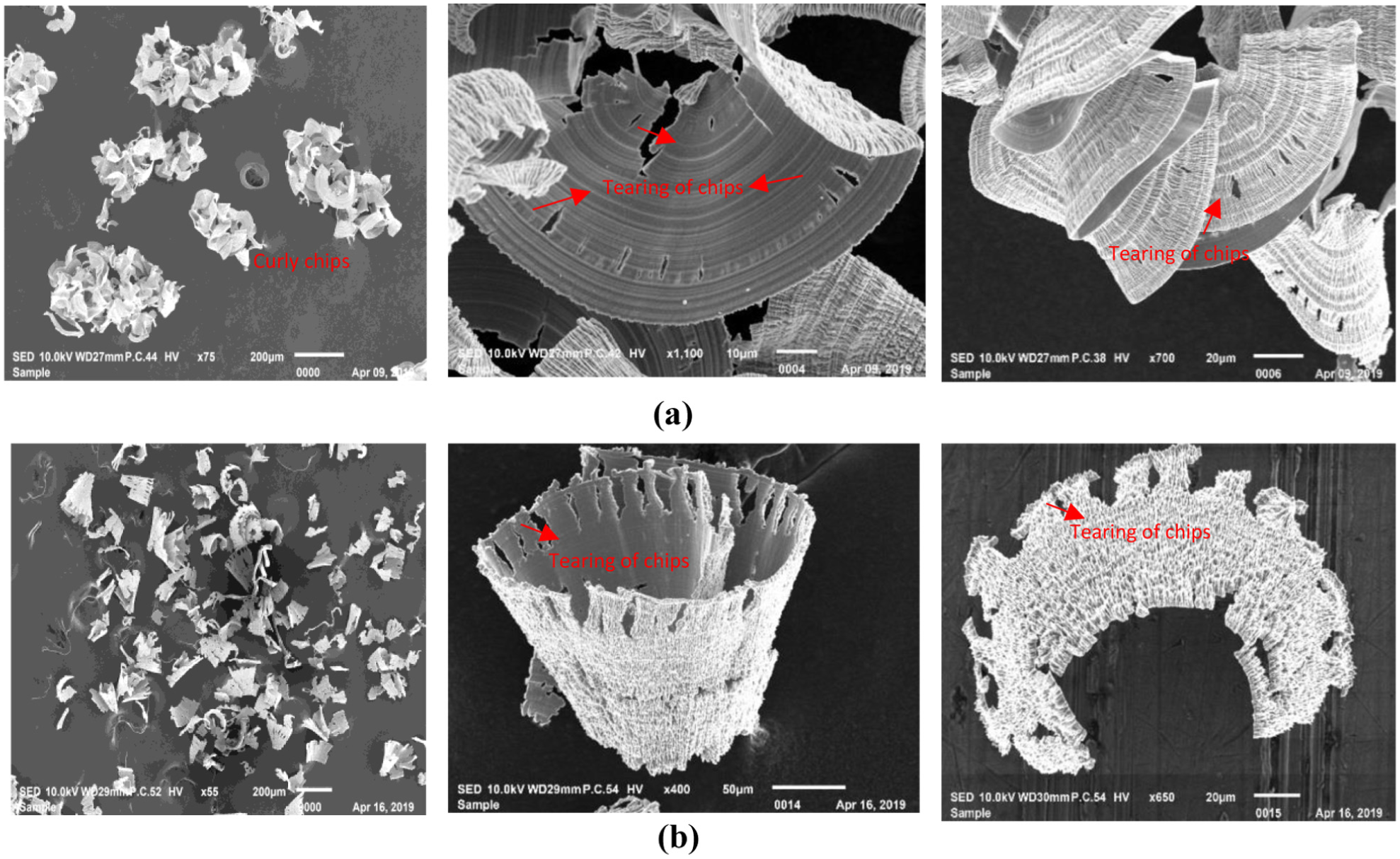
Chip morphology of Ti6Al4V obtained at feed rates (velocity of the tool against rotating workpiece) of: (a) 5 mm/min and (b) 1 mm/min. 13
While these chips exhibit a curl shape, they also display varying-sized periodic cracks. Recent AM-focused work on Ti–6Al–4V (e.g. TPMS lattices produced by L-PBF) shows pronounced orientation-dependent mechanical anisotropy of the AM microstructure, which can influence downstream machining and surface integrity; this provides a process–structure backdrop for interpreting the mechanism differences we observe in diamond-turned AM Ti6Al4V. 11 This study used advanced microscopic characterisation tools to understand the nuanced aspects of this unique chip formation mechanism for an improved understanding of the surface integrity of the machined surface.
The novelty of this work lies in two aspects: (i) it establishes, for the first time, that redeposited debris observed in diamond machining of additively manufactured Ti6Al4V is not the result of carbide formation or precipitation as previously reported, 16 but instead originates from a solid-state friction-induced welding mechanism without phase transformation; and (ii) it reveals a continuous plastic chip formation process with intermittent fractures, in contrast to the adiabatic shear-driven saw-tooth chips typically reported for cast Ti6Al4V.14,15
The purpose of this work is to establish a mechanistic link between chip formation processes and the resulting machined surface integrity in additively manufactured Ti6Al4V during diamond machining. By clarifying how continuous plastic chip flow with intermittent fracture transitions into redeposited debris through friction-induced welding, this study provides direct evidence for the origins of surface protrusions that degrade optical finish. The benefit of identifying this relationship is twofold: (i) it enables predictive understanding of how chip-level dynamics govern final surface quality, and (ii) it highlights that suppressing friction-induced welding is a critical requirement for achieving nanometric finishes in AM Ti6Al4V mirrors. These insights not only extend the fundamental knowledge of machining AM alloys but also guide the development of tool designs, lubrication strategies or hybrid finishing processes for high-precision optical and biomedical components.
We conducted a series of precision machining trials on additively manufactured Ti6Al4V specimens and observed a consistent pattern on the machined surfaces. These patterns appeared as protrusions on the surface, resembling redeposited metal debris particles. These deposits were seen to contribute to the deterioration of surface roughness quality. The remainder of this work investigates the origins and characteristics of these metallic protrusions using advanced microscopy techniques.
Experimental details
Additive manufacturing of the Ti6Al4V ELI samples
The additive manufacturing of Ti6Al4V wafers was carried out using the Selective Laser Melting (SLM) process on an EOS M290 3D printing system. 17 This system is equipped with a Nd-YAG fibre laser operating at a maximum power of 400 W and a wavelength of 1070 nm, 18 with a spot diameter of 80 µm. The quality of the printed parts is known to depend on various processing parameters, including laser power, hatch spacing and laser scan speed. 19 Additionally, the quality of the build is also governed by factors such as particle size, shape, preparation method, surface morphology and conditioning play a crucial role in determining the final build quality. For this study, EOS titanium Ti6Al4V Grade 23 powder was used.
The microscopic characterisation of the sourced powders showed spherical particles with an average size of about 37 µm.18,20 Details of an extensive parameter optimisation exercise for the additive manufacturing of Ti6Al4V ELI alloy have been reported previously and are not repeated here for brevity.17,18,20 Through a series of trials, the optimal parameters for the Selective Laser Melting (SLM) process were determined as laser power of 250 W, laser scan speed of 1500 mm/s, hatch spacing of 0.2 mm, layer thickness of 30 µm and a build plate temperature of 35°C. 21 3D printing process was conducted in an argon gas environment to prevent oxidation.
After fabrication through the SLM process, all specimens were heat-treated at 800°C for 2 h, followed by annealing at 300°C for 4 h to improve their material properties. 20 A wire-cut-EDM process was then used to cut and separate the samples from the baseplate. To smooth the part surface quality, a lapping process was employed, which provided a moderate Ra of about 1.5 ± 0.5 µm.
Diamond machining of the additively manufactured Ti6Al4V samples
Post completion of the 3D printing, the parts were precision machined using a single-point diamond machining process. An ultra-precision three-axis CNC lathe machine (Model: Precitech Nanoform 200) was used to perform the precision machining activity. Monocrystalline diamond cutting tools (supplied by Contour Fine Tooling, UK) with dodecahedral orientation and a conical clearance design, featuring a rake angle of 0°, a clearance angle of 10° and a nose radius of 1 mm, were used for machining. Various machining parameters were explored, including spindle speeds ranging from 2000 to 4000 rpm, feed rates between 1 and 5 mm/min and depths of cut from 1 to 10 µm. The optimal surface finish was achieved using a spindle speed of 2000 rpm, a feed rate of 5 mm/min and a depth of cut of 10 µm. 13 A sequence of operations performed as part of this work, starting from the powder to the finished machined wafer, is shown in Figure 2.
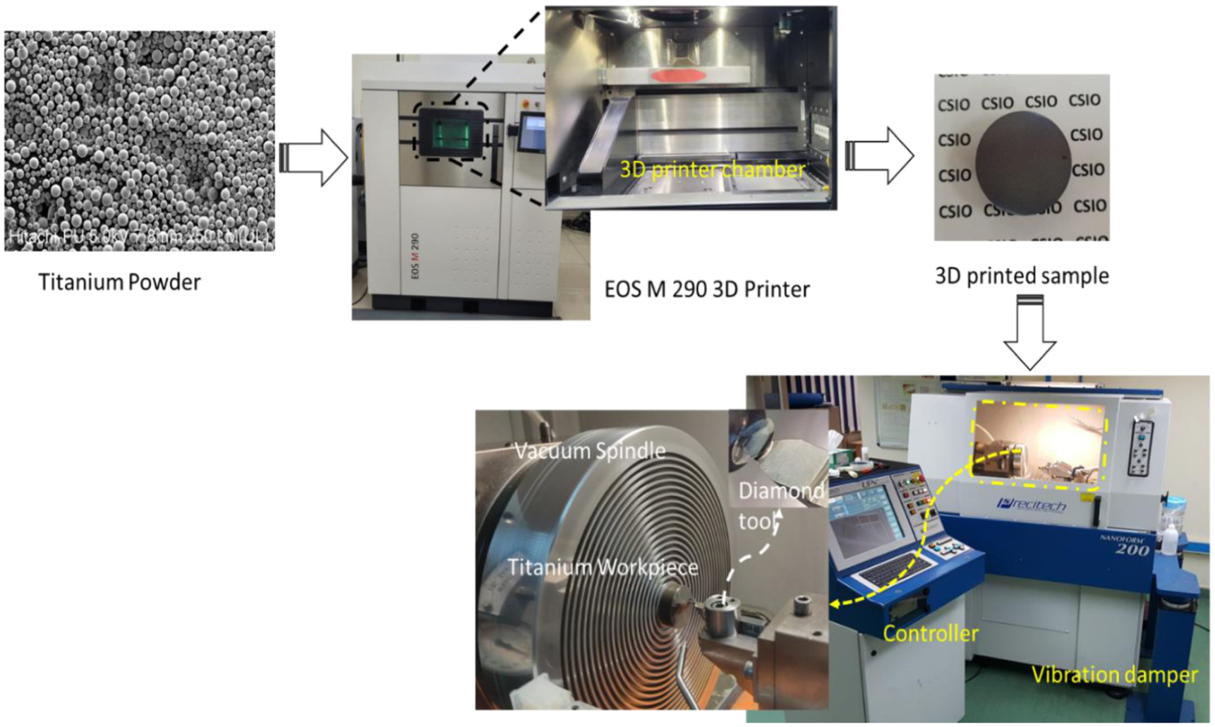
Manufacturing protocol and sequence followed to fabricate and machining the Ti6Al4V ELI alloy. 13
Materials characterisation
Phase analysis of the additively manufactured circular disc or ingot was performed using X-ray diffraction (Bruker D8 Focus) with a Cu Kα wavelength (λ = 1.54056 Å) and a step size of 0.01°. The manufactured surfaces were examined using a Keyence digital optical microscope (Model: VHX-700N, UK).
Specific features of the diamond-turned surface were analysed in greater detail. A cross-section slice was prepared using an FEI Helios NanoLab Focused Ion Beam (FIB) system. This cross-section was subsequently examined using a Transmission Electron Microscope (FEI Tecnai G2) operated at 200 kV. High-resolution lattice fringe images were analysed using Gatan® Digital Microscope software to provide detailed insights into the surface structure and characteristics.
Results and discussions
Initially, the X-ray diffraction (XRD) pattern was recorded to determine the crystallographic phase of the manufactured Ti6Al4V ingot. The analysis revealed that the crystal structure of Ti6Al4V was predominantly hexagonal, consistent with the reference pattern (PCPDF No. 00-001-1197). This structure matched the crystal phase of the parent metal powder, indicating no significant phase transformation during the manufacturing process, as shown in the recorded diffraction data in Figure 3.
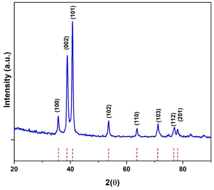
X-ray diffraction pattern of as-manufactured Ti6Al4V ingot.
The manufactured ingot, shaped as a circular disc, was examined using a digital optical microscope (see Figure 4(a)). The surface distinctly displayed the layered architecture characteristic of the SLM process, as further illustrated in Figure 4(b) to (d). After undergoing single-point diamond turning, the wafer achieved a mirror-finished metallic lustre, as shown in Figure 4(e). However, the machined surface exhibited the presence of surface structures in the form of redeposited debris. One such particle was measured to be approximately 10–20 µm in diameter with a height ranging from 5 to 20 µm. An optical image of this metallic debris particle is presented in Figure 4(f), along with its corresponding height profile in Figure 4(g). These structures appeared fully intact on the machined surface. In contrast, the surface quality achieved after the lapping process (reference lapping post-processing) retained the parent material’s colour and showed no debris. Nonetheless, the surface was uneven, as depicted in Figure 4(h) to (i).
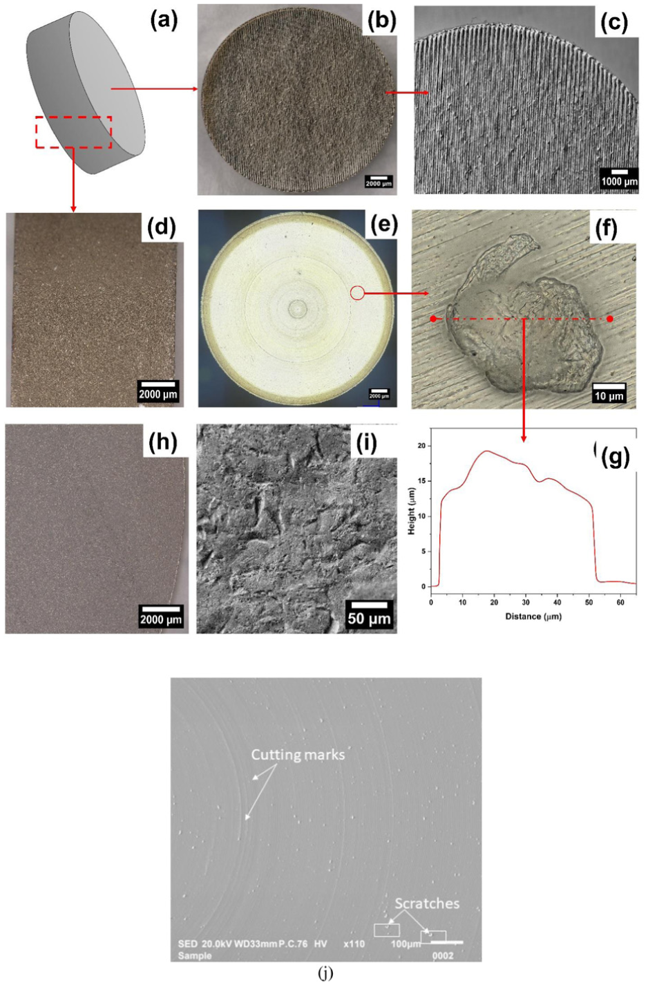
Optical micrograph of Ti6Al4V sample:(a) schematics of additive manufactured Ti6Al4V ingot,(b) manufactured surface cross-section face, (c) enlarged view of micrograph b, (d) optical micrograph of side face, (e) diamond turned surface, (f) debris particles on the diamond turned surface, (g) height profile of debris marked on image f, (h) surface of Ti6Al4V obtained from the lapping process, (i) magnified view of the lapped surface and (j) SEM image showing significant redeposited metal debris particles.
Recent literature suggests that the presence of redeposited debris particles may be attributed to the effect of precipitation. 16 Previous molecular dynamics studies have proposed a mechanism in which dynamic hard particles, significantly stronger than the parent metal, are formed as a result of carbide reactions from diamond. This mechanism was suggested to play a key role in governing groove wear of the diamond-cutting tool.22,23 In the current investigation, however, the volume of tool wear was found to be significantly smaller than the volume of the redeposited debris particles, even when accounting for the stoichiometry of titanium and carbon that could form titanium carbide. Therefore, the possibility of the debris being titanium carbide can be ruled out.
The present findings complement the recent mechanism-level analyses of AM Ti-6Al-4V lattice structures,11,12 which related anisotropic deformation and density gradients to mixed brittle–ductile fracture and controlled collapse behaviour. In contrast to these quasi-static observations, the current study identifies that tribological friction during high-speed cutting initiates a solid-state welding mechanism at the nanoscale, producing local adhesion and surface protrusions. This indicates that the thermomechanical stress fields generated under diamond turning can activate deformation pathways analogous to those seen in layer-wise collapse, yet manifested here as bonding rather than failure – linking chip formation dynamics, frictional heat and surface integrity.
The next stage of the investigation focused on characterising the metal debris for potential phase transformations during the diamond-turning process. A cross-sectional slice of the debris particle, initially 200 µm thick, was prepared and thinned down to 20 nm. The stepwise process of FIB slicing is shown in Figure 5(a) to (e). Figure 5(e) and (f) present a schematic highlighting how the debris protrudes from the diamond-turned surface.
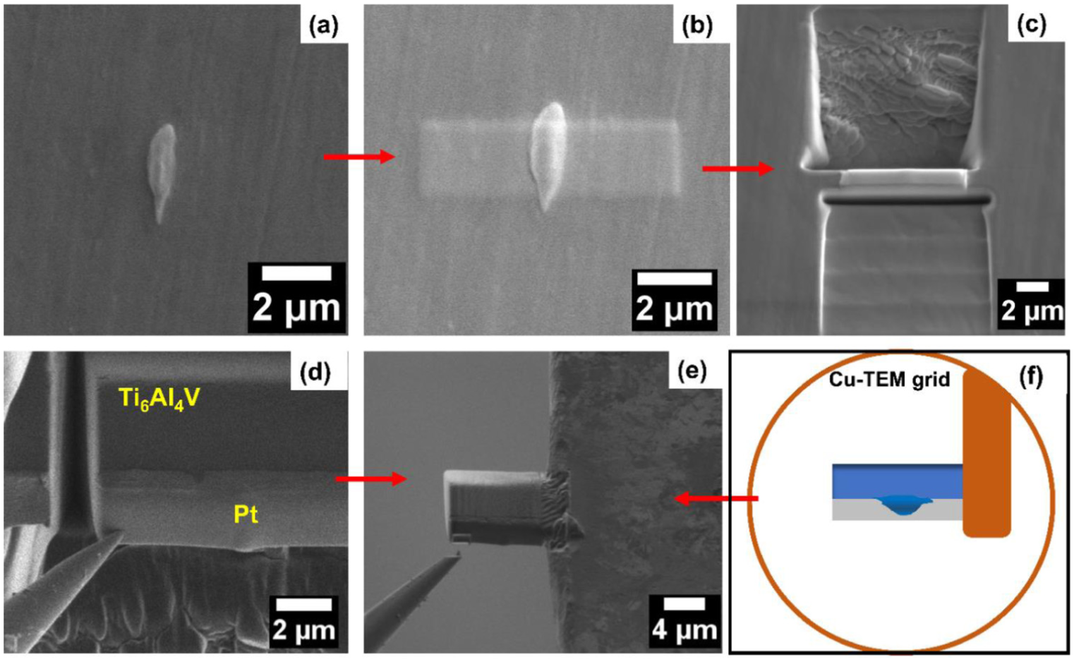
Focused ion beam (FIB) sample preparation stepwise FESEM micrograph, (a) selected debris chip over the diamond-turned surface, (b) deposited Pt over the selected feature to protect its nature from beam damage, (c) digging around forcross-section slice of the feature, (d) a cross-section slice lifted, (e) cross-section slice welded with the Cu-TEM grid and(f) a schematic of a welded slice to the Cu-TEM grid.
Contemporary advances in tool geometry and mechanism analysis for challenging materials (for instance, biomimetic stepped tool designs and composite micro-milling simulations) underline the value of tailored tool/process strategies for mitigating damage and redeposition, a perspective that supports developing targeted approaches to prevent friction-induced welding during diamond machining of AM Ti6Al4V. 3
In Figure 6(a), the sample of the machined surface and its cross-section is shown, with the machined surface marked as the datum using a red dotted line. The protruding structure is visible as the blob extends into the protected Pt layer. A selected area electron diffraction pattern from the bulk material, deep inside the machined surface, is presented in Figure 6(b), along with the corresponding diffraction intensity profile in Figure 6(c). The selected area diffraction ring pattern confirms the nanoscrystalline structure and this pattern also aligns with the X-ray diffraction pattern of bulk materials shown in Figure 3, confirming the consistency of the phase.
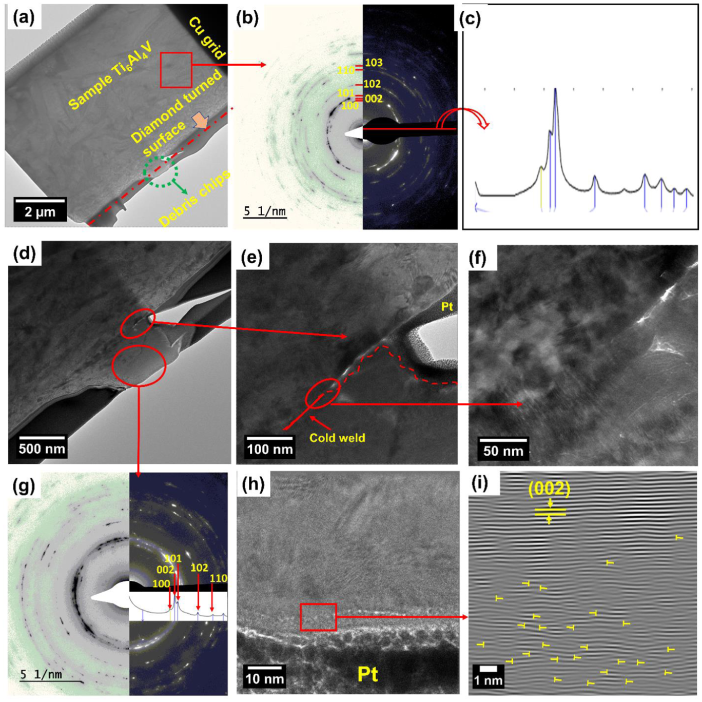
Transmission electron microscope image, (a) Bright-field image of thin-slice from the machined surface with the protrude structure, (b) selected area diffraction pattern from deep inside the machine surface, (c) intensity profile of ring diffraction pattern, (d–f) bright field image of protrude structure, (g) selected area ring diffraction pattern from the protrude structure, (h) high-resolution TEM image from debris chip underneath the platinum and (i) HRTEM FFT filtered image from the marked area in image (h).
Similarly, the selected area diffraction pattern from the debris structure or protrude, shown in Figure 6(g), closely matches that of the bulk material, indicating that the phase remained unchanged during the diamond machining process.
Figure 7(a) to (c) shows the cross-section of the debris structure, revealing that the chips are separate from the machined surface. The debris structure exhibits high porosity, with regions showing both partial and complete friction welding-induced bonding. Notably, any granular structure is absent, confirming that the debris has a microstructure similar to that of the parent material, Ti6Al4V, and has been welded to the machined surface. This observation indicates that no distinct, hard phases have segregated from the parent material.
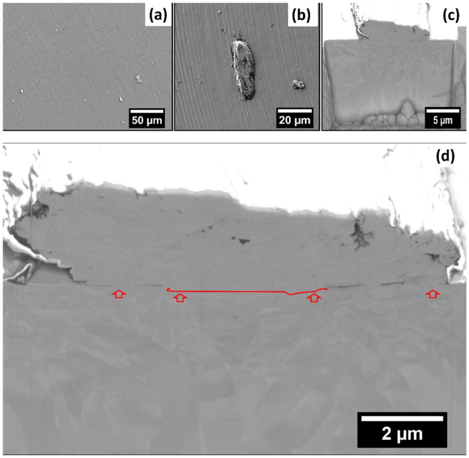
FESEM micrograph: (a) diamond-turned surface micrograph, (b) protrude structure on the diamond-turned surface, (c) Cross-section micrograph of protrude chips cut by Focused ion beam and (d) enlarged view of a cross-section of protrude chip over diamond-turned surface.
The nature of the bonding between the debris and the parent material is further illustrated in Figure 7(d), where some areas show atomic merging with the parent material, while others remain intact with no welding or demonstrate partial bonding.
Conclusions
Metallic mirrors made from Ti6Al4V are gaining popularity across various sectors, including aerospace for optical systems in satellites, telescopes and laser guidance systems; healthcare for surgical tools and diagnostic instruments requiring reflective, biocompatible surfaces and the energy sector for high-stress environments such as laser processing systems and solar reflectors in concentrated solar power setups. Traditional manufacturing methods, such as casting, contribute to significant energy loss and emissions. A more sustainable approach involves combining additive manufacturing with diamond machining, achieving an average surface roughness of approximately 11.8 nm. While this results in good roughness values, the surface integrity of the mirrors consistently reveals a recurring pattern that degrades the overall surface quality. This study aims to investigate the origins and contributions of this pattern through detailed microscopic analysis with techniques such as XRD, TEM and SEM. Specifically, the machined surface exhibited significant protrusions of redeposited metal debris. Contrary to the established theory that titanium precipitation or carbide formation resulting from diamond tool wear might account for these masses, the study identified solid-state friction-induced welding of titanium debris onto the cut surface occurring without phase transformation of titanium. The welded region showed a mix of partially bonded and fully bonded regions. Notably, this phenomenon was not observed when the same materials were lapped and polished.
Overall, this work provides the first mechanistic evidence that debris redeposition during diamond machining of additively manufactured Ti-6Al-4V results from a solid-state friction-induced welding process rather than from carbide formation or precipitation. This observation extends recent studies on deformation and fracture mechanisms in architected Ti-6Al-4V by demonstrating that tribologically driven interfacial bonding can occur without thermal phase change. The discovery introduces a new framework linking AM microstructure, tool–chip tribology and surface integrity, thereby informing process optimisation for optical-grade machining of titanium alloys.
A central outcome of this work is to demonstrate the link between chip formation and machined surface integrity. Specifically, the continuous-plastic-flow chips interspersed with fracture sites generate loose debris that subsequently undergoes friction-induced solid-state welding, producing the characteristic protrusions observed on the diamond-turned surface. Establishing this causal relationship provides a scientific basis for why optical-grade finishing remains challenging in AM Ti6Al4V and points directly to strategies such as suppressing debris welding or controlling fracture-chip formation that can mitigate surface defects. Thus, the study not only identifies a new phenomenon but also delivers actionable insights for advancing the precision manufacturing of AM titanium mirrors and components.
Thus, a major conclusion of the study is that friction-induced welding can act as a precursor to the quality of the finish of additive parts, which represents a substantial challenge to achieving high-quality machining. Overcoming this issue will require the development of hybrid manufacturing strategies to address the precision machining difficulties associated with additively manufactured materials.
Footnotes
Author contributions
SG: Conceptualisation, writing – original draft; NKK: Analysis and editing the draft; NK, RA and AA: Editing the draft.
Funding
The authors disclosed receipt of the following financial support for the research, authorship, and/or publication of this article: All authors would like to thank Dr. Vijay Meena, at CSIO for his help in providing the technical support in 3D printing. All authors acknowledge the financial support provided by the UKRI via Grant No. EP/T024607/1 and the Newton Fellowship award from the Royal Society (NIF\R1\191571). We are particularly grateful to the Royce PhD Equipment Access Scheme, enabling access to the TEM facilities at Royce@Cambridge via UKRI Grant EP/R00661X/1.
Declaration of conflicting interests
The authors declared no potential conflicts of interest with respect to the research, authorship, and/or publication of this article.