
Abstract
This work uses molecular dynamics to simulate the grooving behavior of optical silica glass. The amorphous SiO2 (silica glass) was fabricated using a melting-quenching process, and the critical cut depth, and mechanism of the chip formation, were explored using a molecular dynamics simulation. The analytical results indicated that the tool edge radius affected the critical cut depth and roughness of the machined surface. A larger tool edge radius had a larger equivalent negative rake angle at the same depth of cut, causing a larger critical cut depth, while producing a smoother machined surface. In addition, the uncut chip thickness affected the tangential force and thrust force distribution weighting of the tool. The temperature field analysis revealed that a groove formed by the chip formation mechanism resulted in a higher workpiece temperature, causing the brittle material to exhibit ductile cutting behavior during the nanogrooving process. However, grooves formed by the scratching-indenting mechanism had a lower workpiece temperature.
Introduction
Various scientific and technological applications require the use of machine parts with high hardness and precision. Machining processes make use of parts with high precision, making the ultra-precision machining of hard and brittle materials a novel research subject. Ultra-precision manufacturing methods, such as lithography for semiconductor processes, can produce accurate components that meet the specific requirements for optical, electrical, and mechanical manipulation. Accordingly, many researchers have studied the nano-cutting behavior of various materials using different methods, either experimentally or through simulations.1–8 Since nano-machining experiments are expensive to perform, suitable parameters for the nano-cutting process are often obtained through simulations. Komanduri et al.9–13 investigated the precision cutting of nanometer-grade material using a molecular dynamic simulation of different single-crystal metals, and examined the effects of the cutting orientation, cutting method, and tool geometry on the cutting behavior. Moreover, the atomic friction behavior of the diamond stylus sliding on single-crystal copper was also discussed. The chip formed in ductile metals undergoes serious plastic deformation through dislocation slippage and/or twinning mechanisms in the shear zone. However, chip formation through dislocation slippage is difficult when using amorphous or brittle materials. When cutting brittle materials, the process of brittle-ductile transition needs to achieve two conditions: an uncut chip thickness smaller than the tool edge radius, and a small enough tool edge radius (nanoscale). However, the brittle-ductile transition mechanism has not been adequately explained. 14 Cai et al. 15 utilized molecular dynamics to simulate the nano-cutting of monocrystalline silicon wafers and investigated the ductile deformation chip formation mechanism during the cutting process of brittle materials. The simulation results demonstrate that the shear stress of the material around the cutting edge decreased as the tool edge radius increased. The lower shear stress could not generate the dislocation emission in the chip formation zone, allowing crack propagation to dominate the cutting process, which implied that the chip formation mode had changed from ductile to brittle. Therefore, the ductile-regime cutting conditions for brittle materials are an important research issue.
Brittle materials such as engineering ceramics, optical glass, and semiconductors, are widely applied in high-tech fields such as electronics, optics, and aviation. Therefore, the systematic research on the machining mechanism and technology of these brittle materials, has important theoretical significance and practical value.
For single-crystal Si cutting, when the ratio of the uncut chip thickness to the tool edge radius is less than the critical value, chip formation occurs via extrusion, and cracks appear at the initial cut, even though the cutting was in ductile mode. 1 In ductile-regime machining, a cut is formed in a brittle material through both plastic deformation and brittle fracture, and the resulting cracks are prevented from extending into the finished surface. Therefore, a damage-region analysis approach was proposed to determine the subsurface damage depth, thereby ascertaining the quality assurance of the machined surface. 2 In the nano-cutting of brittle materials, most of the studies focused on Si-machined behavior because of semiconductor processes. The issues investigated in Si nano-cutting include the crystallographic effect, 3 crack behavior, 4 geometry of the cutting tool, cutting conditions, 5 material side flow on surface quality, 6 size effect of tool edge in the ductile cut region, 7 phase transformation in the chip formation zone, 16 and effect of the cutting edge radius on a machined surface. 17
Silica glass is currently one of the most important materials and is indispensable for the further development of technology. Transparent and opaque silica glasses have many applications, including optics, medicine, and space technology. 18 However, inadequate research has been done on the cutting behavior of silica glass compared to that of Si. Chen et al. 19 studied the effect of the crystal orientation on the cutting behavior of single-crystal SiO2. For practical applications, amorphous silica is widespread and easily obtainable. Therefore, this study focuses on the nanogrooving behavior of amorphous silica to better understand the nano-cutting behavior of this material. The groove formation mechanisms under different cut depths are discussed, and the critical dimension of the uncut chip thickness when cutting amorphous silica, which could form a continuous chip, was studied using the molecular dynamics (MD) method. The statistical mechanical theory was employed to determine the physical properties of the overall system, such as the stress and temperature distribution.
Simulation methodology
In this investigation, MD simulations were performed using a large-scale atomic/molecular massively parallel simulator (LAMMPS), 20 and the Ovito 21 software application was used to observe the movement trajectories of atoms, and the mechanism of deformation.
Fabrication of amorphous quartz glass
SiO2 has a tetrahedral arrangement in which one silicon atom is bonded to four oxygen atoms. Most oxygen atoms are bonded to two silicon atoms, such that the two tetrahedra meet and form a point (bridging atoms); and others are bonded to only one silicon atom (non-bridging atoms). However, the orientation can be random, leading to an amorphous structure. The ratio of bridging atoms to nonbridging atoms determines the “quality” of the silicon dioxide. If all oxygen atoms are bridging atoms, a regular crystal structure is formed (quartz). 22 To establish an amorphous silica model, a bulk material system was modeled using a tetrahedral structure comprising four oxygen atoms and a silicon atom, in which the tetrahedral structures were bridged by one oxygen atom. The basic unit of SiO2 is depicted in Figure 1.
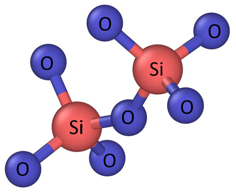
Schematic of the SiO2 unit and bonds.
The relaxation process for the material system in this simulation was performed at an initial temperature of 300 K using the NVT ensemble. During the melting process, a periodic boundary condition was applied in all three directions of the material system.
23
Figure 2(a) depicts the crystallized quartz model before melting was done at a temperature of 300 K. The model was then heated to 3000 K at a rate of
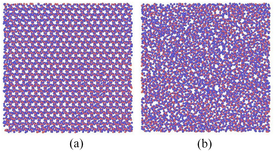
Different crystal structure of SiO2 model: (a) crystallized quartz and (b) amorphous silica glass.
Potential function
In MD simulations, the interatomic force is related to the potential function. The potential function is a semi-empirical formula obtained from quantum mechanics and spectroscopy experiments, and can be utilized to obtain the intermolecular forces and related material properties. Therefore, the selection of the potential function is important for the description of the material properties, as it affects the accuracy and reliability of the simulated results.
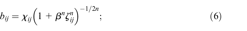
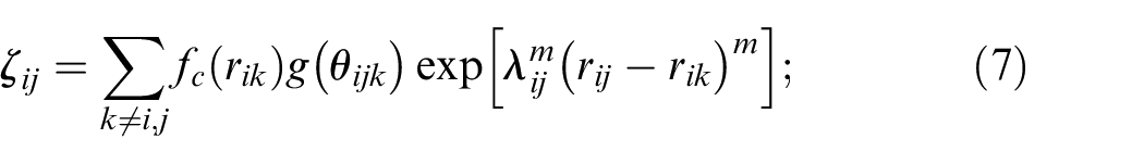
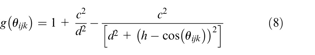
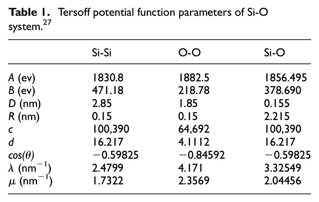
The three-body Tersoff24–26 potential was originally proposed to study the different phases and deformation behavior of silicon. Munetoh et al. 27 extended this potential function to describe the Si---O system. The formulas defining the Tersoff potential for the Si---O material system are as follows.24–28


Here, E denotes the total energy of the system,
Tersoff potential function parameters of Si-O system. 27
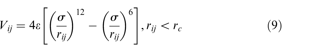
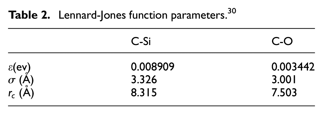
Here, Vij denotes the potential energy between atoms i and j, ε is the binding energy, σ is the length scale representing the distance at which the intermolecular potential between the two atoms is zero, rij is the distance between the atoms i and j, and rc is the cutoff radius. The relative parameters are listed in Table 2.
Lennard-Jones function parameters. 30
Cutting conditions
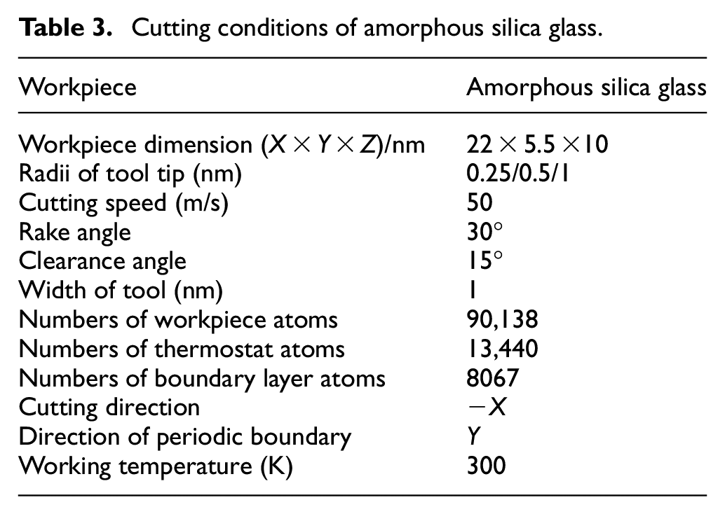
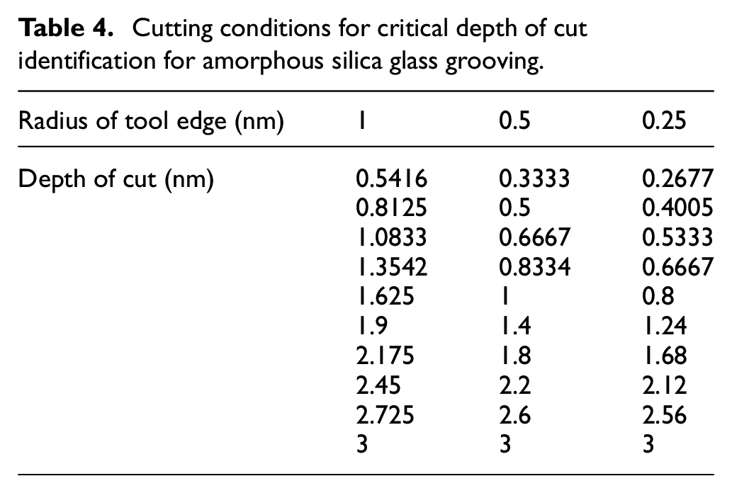
To simulate the grooving process of amorphous SiO2, the workpiece was constructed using a boundary layer, a thermostat layer, and a working region. Diamond tools with different edge radii were used for cutting. A diamond structure composed of carbon (C) atoms was selected as the cutting tool, with the cutting tool being treated as a rigid body since the main purpose of this research was to explore the ductile cutting problem of brittle materials. Therefore, this study does not consider the tool deformation. Figure 3 illustrates the simulation model. The atoms forming the boundary layer were fixed at their respective crystal positions to reduce boundary effects and maintain lattice symmetry. During the cutting process, the mechanical work done by the cutting tool was transformed into heat energy through internal (plastic deformation) and external (rubbing) friction mechanisms. Thermostat atoms conducted heat from the workpiece during the cutting process, with additional heat being carried away by the chip during machining. The simulation of the grooving process was conducted after the system had reached equilibrium. To obtain the critical cut depth (minimum uncut chip thickness for chip formation), more simulation conditions, obtained from pretests, were required (up to 30 cases), as listed in Tables 3 and 4, and found to be suitable.
Cutting conditions of amorphous silica glass.
Cutting conditions for critical depth of cut identification for amorphous silica glass grooving.
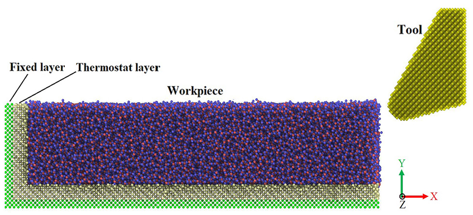
Schematic of the MD simulation model.
Temperature field evaluation
A single atom was centered using the truncation radius method, utilizing the average kinetic energy of all atoms in the cutoff radius, which is regarded as the kinetic energy of the central atom. Thus, the temperature of the central atom (
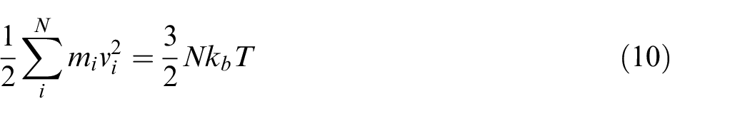
where N denotes the number of atoms in the cutoff region; mi and vi represent the mass and resultant velocity of the ith atom, respectively;
Results and discussions
Characterizations of the amorphous quartz glass workpiece
To measure the workpiece crystallinity, radial distribution function (RDF) was adopted to characterize the silica glass during the quenching process. Figure 4 shows the changes in the RDF of the workpiece between the molten (2040 K) and solid states (300 K) at various temperature levels. The heat capacity of the material continuously changes as the heated material changes from a molten to a solid state, indicating a second-order phase transition. During the cooling process, the molecular chain in the material system was able to only generate local motion once the glass transition temperature was reached. According to Ojovan, 31 the glass transition temperature of amorphous silica glass is 1475 K . In this study, the characterization of the RDF showed that the second peak was gradually formed during cooling, due to the temperature of the workpiece being lower than the glass transition temperature (when the temperature was lower than 1426 K). Consequently, the rapid cooling reduced the crystallization time, causing the workpiece to retain an amorphous state until the temperature fell to 300 K.
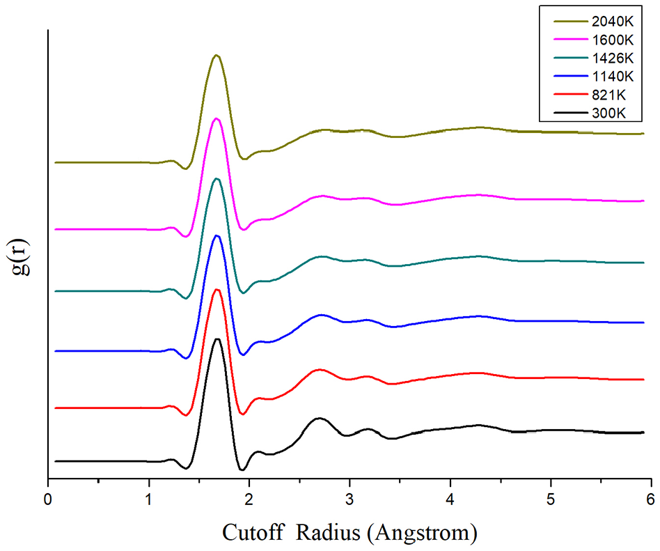
RDF distribution at different temperatures during the quenching process.
Critical cut depth and groove formation mechanism
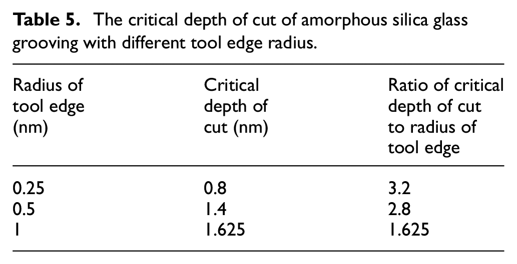
In the brittle material cutting process, the uncut chip thickness needs to be as small as possible to obtain ductile cutting behavior. However, chip formation cannot be completed if the uncut chip thickness is lower than the critical uncut chip thickness. Therefore, the cutting process was changed to scratching-indenting (plowing), as depicted in Figure 5(a). When the uncut chip thickness exceeded a critical value, a chip was formed which flowed over the rake surface of the tool, as shown in Figure 5(b). Therefore, the critical uncut chip thickness is a significant parameter in the brittle material cutting process, with different combinations of materials and tool edge radii producing different critical uncut chip thicknesses. Table 5 lists the critical cut depths for amorphous SiO2 grooving using different tool edge radii, as obtained through the simulation analysis of different cutting conditions. The critical cut depths of the tools increased with increasing tool edge radius. Because of the tool edge radius effect, tools with larger tool edge radii had larger equivalent negative rake angles, at the same depth of cut and boundary condition (as shown in Figure 6). However, the ratio of the critical cut depth to the tool edge radius was smaller when the tool edge radius was larger, as indicated in Table 5. This implies a disproportionate relationship between the critical cut depth and tool edge radius, with the ratio tending to decrease as the tool edge radius increased. This trend is similar to that observed in a previous study, where micro-cutting of the chip can be formed even though the uncut chip thickness is less than the radius of the tool edge, and the chip formation mechanism is different. 32
The critical depth of cut of amorphous silica glass grooving with different tool edge radius.
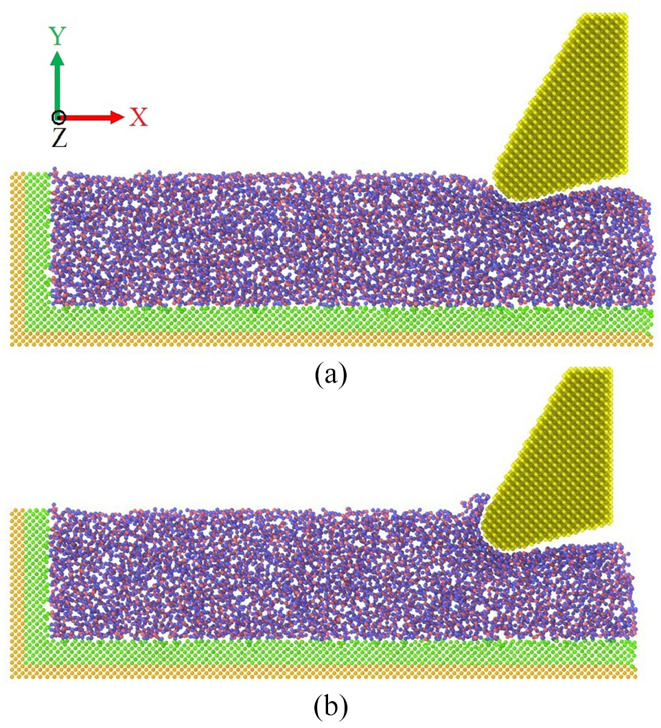
Longitudinal cross-section of the grooving workpiece at different depths of cut using cutting tool with edge radius of 1 nm: (a) 0.8 nm/no chip formation and (b) 1.9 nm/chip formation.
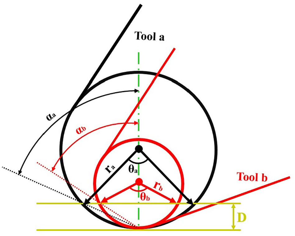
The equivalent rake angle of the tools with different edge radii at the same depth of cut D.
The results of the grooving process showed that the depth of the groove was less than the cutting depth, implying that there was an elastic recovery phenomenon at the bottom of the groove. To obtain a more accurate nanogroove dimension, the elastic recovery was measured under different grooving conditions, as shown in Figure 7. The results indicated that the elastic recovery approaches a constant when the uncut chip thickness exceeds the critical cut depth; with a smaller tool edge radius producing a lower elastic recovery. This can be explained using contact mechanics, which states that for a constant load, a smaller contact radius causes higher contact stress and results in more plastic deformation in the contact region. Moreover, for the groove formed by the scratching-indenting mechanism, the highest elastic recovery was reached when the cutting depth was just lower than the critical cut depth.
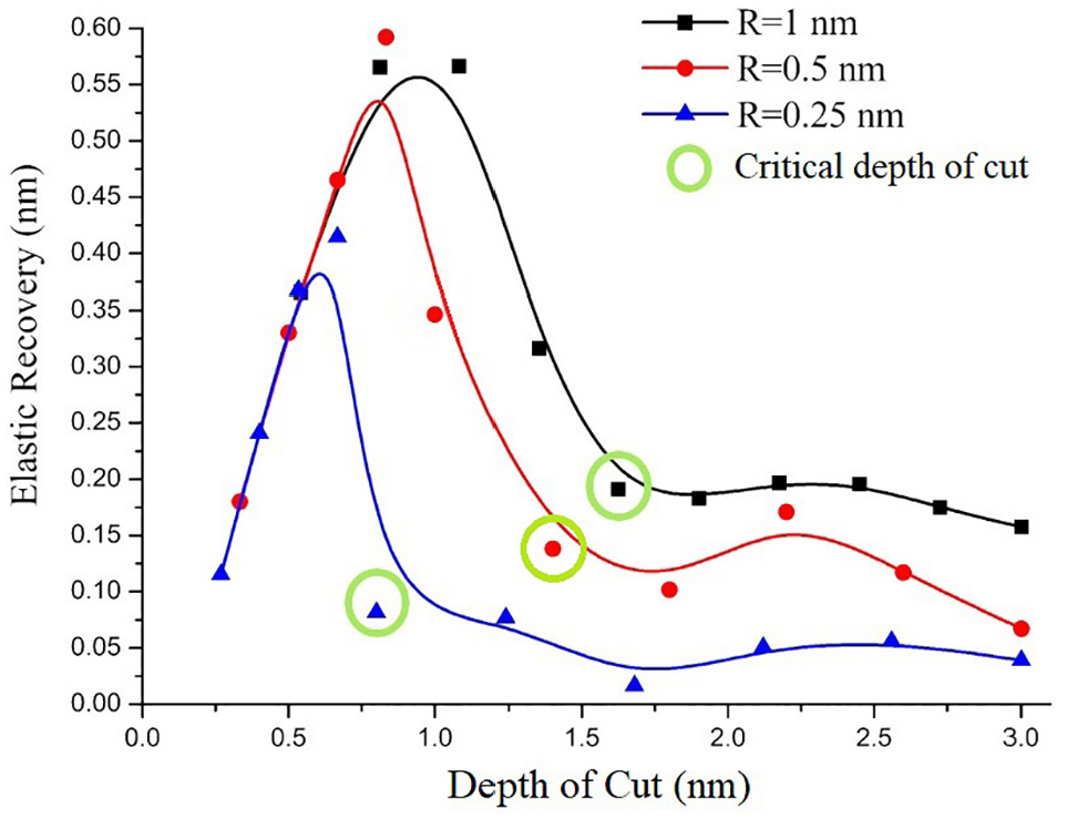
Relationship between depth of cut and elastic recovery of the groove bottom at different grooving conditions.
Additionally, the surface roughness of the bottom of the groove revealed that the surface roughness decreases with an increase in the tool edge radius, as shown in Figure 8. This was due to the large radius of the tool edge, which created a large contact length between the tool and the workpiece, and increased the negative rake angle (Figure 6). This caused a burnishing effect at the bottom of the machining groove during the cutting process, which could, in turn, densify the machined layer of the material and cause the fill-up of the microvoids with surface atoms, improving the surface roughness and enhancing the plowing effect through the use of a large tool edge radius.
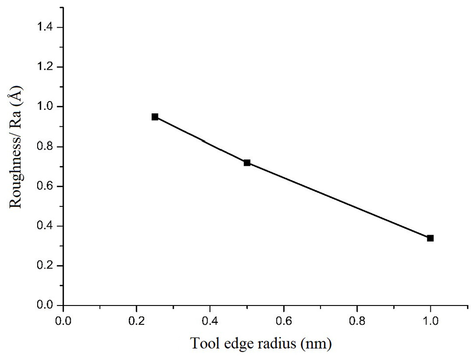
The relationship between different tool edge radius and surface roughness (Ra) of grooved bottom at a depth of cut 2.1 nm.
Temperature field and subsurface structure under different cutting conditions
During the cutting process, the work done by the tool is transformed into the energy required for material deformation, and is inclusive of the internal and external friction energies between the atoms. Figure 9 depicts the typical temperature distribution in the workpiece at different cut depths (0.8 and 1.9 nm) during the grooving process for a tool edge radius of 1 nm. The temperature rise was only significant when the chip formation mechanism was operating under the shear effect, but not when no chip was formed and the groove was formed by the scratching-indenting mechanism. Under the plowing condition, the chip was not formed, resulting in less plastic work than in the case of chip formation. The internal frictional work by the moving atoms in the plowing condition was less than that in the chip formation mode, and the temperature increase of the workpiece was not significant, as shown in Figure 9(a). Conversely, the temperature was very high in the region in front of the tool tip in the chip formation condition, as shown in Figure 9(b). Previous investigations have demonstrated that metal micro-cutting forms a very small triangular zone (dead metal zone) in front of the tool tip. 32 At the tip of the triangular zone, the material flow is separated into two directions along the boundaries of the dead zone, and two material-flowing regions (slipping and plowing effects separately) were observed. One region covered the upper edge of the triangular zone up to the rake face, and the other covered the bottom edge of the triangular zone. Therefore, the dead zone had a high temperature due to the severe internal friction at its boundary. Additionally, chip formation caused serious plastic deformation in the primary shear zone, resulting in a high temperature in this region. As shown in Figure 9(b), the high-temperature region in the workpiece included the primary shear zone and the dead zone. The relationship between the temperature and friction work (internal and external) clearly reveals that at a constant cutting speed, regions with greater plastic deformation in the workpiece have higher temperatures due to the internal friction motion of the atoms.
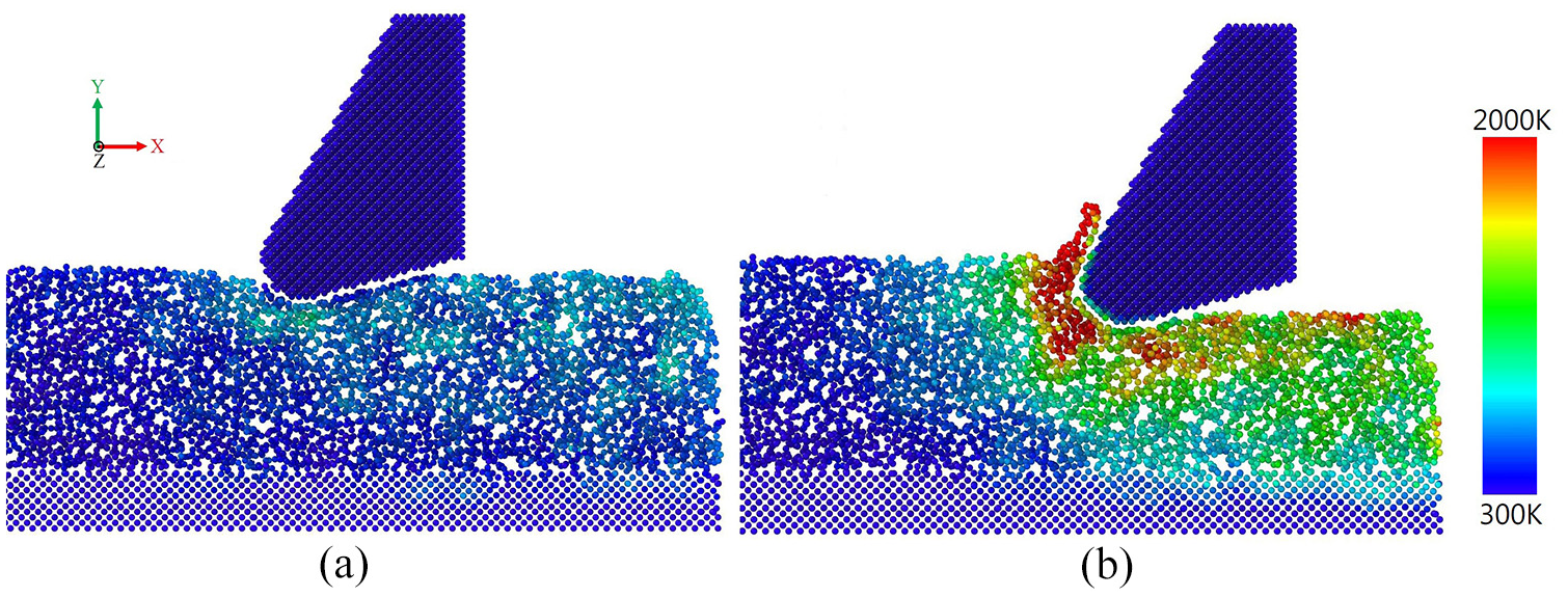
Temperature distribution in longitudinal cross-section of the grooving workpiece using tool with edge radius of 1 nm at different depths of cut: (a) 0.8 nm and (b) 1.9 nm.
Guo et al. 33 found that the scratched surface of quartz glass has a densification layer that is immediately adjacent to the scratched surface, resulting from the reduced microscopic cavity in the silica glass. The densification layer was identified in the subsurface of the bottom of the groove. Figure 10 shows the typical RDF characterization on the bottom of the groove at different depths of cut using a tool with an edge radius of 0.5 nm. The cut depth is represented by the black line (0.6667 nm), which is less than the critical cut depth; the red line (1.4 nm) reaches the critical cutting depth; and the blue line (1.8 nm) is greater than the critical cut depth. From the figure, among all the cutting conditions, the highest peak of RDF characterization occurred when the uncut chip thickness was less than the critical cut depth, showing that the density in this region was the highest. As the uncut chip thickness approached the critical depth, the bottom of the groove was denser and the amount of elastic recovery was higher (as shown in Figure 7). When the cut depth exceeded the critical cut depth, the degree of densification was reduced because the chip formation mechanism dominated the grooving process, which also decreased the RDF value. This is due to the indenting-sliding effect being reduced.
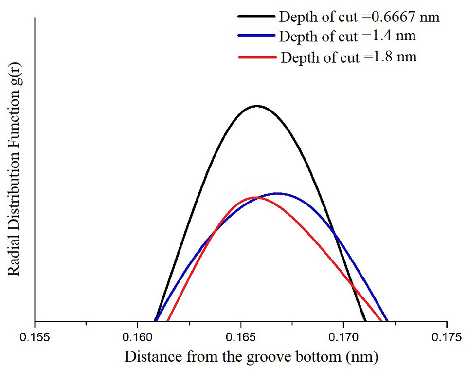
Results of RDF characterization of the grooved bottom at different depths of cut using a tool with edge radius of 0.5 nm.
Cutting force analysis
During the cutting process, the tool was subjected to a tangential force (in the x-direction), thrust force (in the y-direction), and lateral force (in the z-direction). The lateral force is caused by the elastic recovery of the grooved walls. The lateral force effect on the cutting process is generally negligible compared to the other forces during the grooving process; therefore, it is not discussed herein. In the cutting process, the uncut chip thickness is an important parameter because it dominates the chip formation behavior and the specific cutting energy (size effect). Figure 11 illustrates the fluctuation of the tangent force (or cutting force) and thrust force at different cut depths during the cutting process.
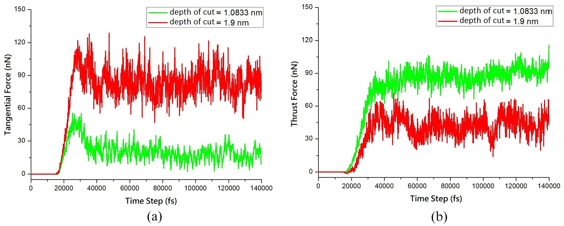
Cutting force of the tool with edge radius of 1 nm at different depths of cut 1.0833 and 1.9 nm: (a) tangential force and (b) thrust force.
Figure 11(a) shows the tangential force acting on the tool with an edge radius of 1 nm, with cut depths of 1.0833 and 1.9 nm for the different conditions, respectively. Figure 11(a) shows that at a cut depth less than the critical cut depth (1.0833 nm), the tangential force increased quickly when the tool was in contact, and then decreased rapidly as the tool tip rode on and scratched over the workpiece surface. Conversely, when the uncut chip thickness was greater than the critical cut depth, the tangential force increased rapidly when the tool was in contact, but decreased slightly during the chip formation period. Comparing the two grooving conditions, the tangential force of chip formation was approximately 4.5 times that of the scratching-indenting condition, because of the different groove formation mechanisms. The serious plastic deformation observed in chip formation required the removal of material, resulting in a higher tangential force. However, in the scratching-indenting condition, the tangential force was mostly due to the friction effect, leading to a lower tangential force. The temperature distributions in both conditions also conform to the results. Nevertheless, the thrust force acting on the tool had different results; that is, the thrust force at an uncut chip thickness less than the critical cut depth was higher than that at an uncut chip thickness greater than the critical cut depth. A comparison of Figure 11(a) and (b) shows that the tool thrust force was higher than the tangential force at an uncut chip thickness less than the critical cut depth, but less than the tangential force when the uncut chip thickness was greater than the critical cut depth. This implies that when the uncut chip thickness was less than the critical cut depth, the groove was formed by scratching effect combined with an indenting effect in the normal direction, causing the displacement of atoms to reduce the microvoids and densify the grooved surface, so that the thrust force was higher than the chip formation mechanism. Furthermore, at the same grooving condition under the chip formation mechanism, a smaller tool edge radius produced a lower thrust force, but did not influence the tangential force, as shown in Figure 12. The thrust force acting on the tool with a larger cutting edge radius was higher than that on tools with smaller radii. This phenomenon was due to the longer contact length between the tool and the workpiece when the tool edge radius was large, which resulted in greater elastic strain recovery (Figure 7) at the bottom of the groove. Combining the influence of the longer contact length of the tool tip with the factors mentioned above (effective rake angle), it can be seen that a larger tool edge radius generated a larger thrust force. However, the cutting force is mainly used to overcome the shear deformation in the shear zone during chip formation, which is dependent on the shear strength of the material. According to cutting theory, under the conditions of chip formation machining, when the cut depth is the same, the magnitude of the cutting force is related to the rake angle of the tool. As shown in Figure 12, the shear strain required for chip formation should be similar because the rake angle of the tool is the same. Thus, when the uncut chip thickness is larger than the critical depth, the tool edge radius has an insignificant effect on the tangential force.
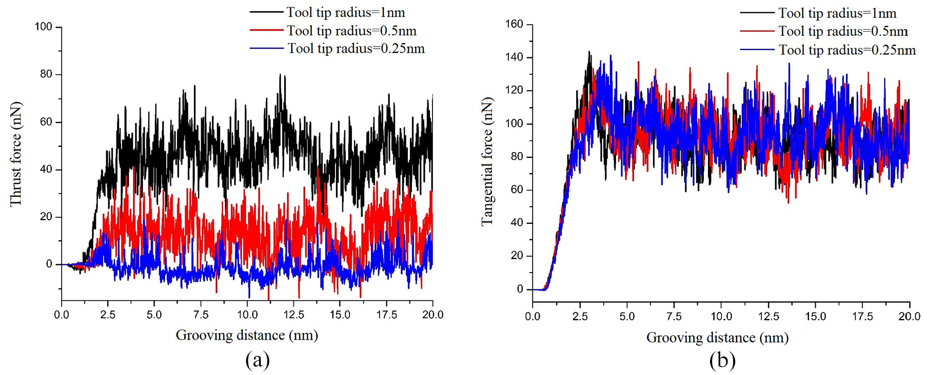
The cutting force of the different cutting tool at depth of cut 2.1 nm condition-chip formation: (a) thrust force and(b) tangential force.
Conclusions
This study examined the nanogrooving behavior of amorphous silica using molecular dynamics simulations. The MD simulation results revealed that nanogrooving of amorphous silica is dominated by the tool edge radius and uncut chip thickness, with various combinations of these having different groove formation mechanisms. The simulation results are summarized as follows.
In the SiO2 amorphous silica nanogrooving process, if the uncut chip thickness is less than the critical cut depth, then the groove-forming mechanism is mainly the scratching-indenting mechanism; if the uncut chip thickness is greater than the critical cut depth, the groove-forming mechanism is mainly through chip formation.
A small tool edge radius results in a small critical cut depth.
In nanogrooving based on chip formation, the machined surface is rougher with a small tool edge radius than with a large tool edge radius.
When the groove-forming mechanism was based on the scratching-indenting mechanism, the tangential force was relatively smaller, but the thrust force was relatively larger. Under this cutting condition, the indenting effect increased the thrust force, with the tangential force being as a result of the friction effect.
In nanogrooving with chip formation, the tangential force is larger than the thrust force. In this condition, a serious shear effect that causes plastic deformation was necessary to form the chip, thereby enlarging the tangential force.
During the nanogrooving process, the temperature field analysis showed that the groove formed by the chip formation mechanism led to a significantly larger temperature rise in the workpiece compared with that formed by the scratching-indenting mechanism.
Footnotes
Acknowledgements
The authors would like to thank the Ministry of Science and Technology of the Republic of China, Taiwan, for financially supporting this research under Contract No. MOST 108-2221-E-011-123-, and the National Center for High-performance Computing (NCHC) of National Applied Research Laboratories (NARLabs) of Taiwan for providing a (computational OR computing) platform.
Authors’ contributions
Yuan-Ching Lin directed this study. Yuan-Ching Lin and Chung-Yen Wu designed the architecture and simulation code of the model, then they carried out the simulations and data analysis. Yuan-Ching Lin wrote the manuscript with the help from Chung-Yen Wu.
Declaration of conflicting interests
The author(s) declared no potential conflicts of interest with respect to the research, authorship, and/or publication of this article.
Funding
The author(s) disclosed receipt of the following financial support for the research, authorship, and/or publication of this article: This research was funded by Ministry of Science and Technology, ROC.
Ethical approval
1. This manuscript did not be submitted to more than one journal for simultaneous consideration.
2. The submitted work is original and did not have been published elsewhere in any form or language.
3. This study did not be split up into several parts to increase the quantity of submissions and submitted to various journals.
4. Results of this study are presented clearly, honestly, and without fabrication, falsification or inappropriate data manipulation (including image based manipulation).
5. This study did not plagiarize data, text, or theories by others are presented as if they were the author’s own.