
Abstract
Electrochemical discharge machining (ECDM) processes have been used to realize miniature structures such as micro-channels and micro-holes on non-conductive materials such as quartz and Pyrex for a variety of applications. However, for realizing mechanical/physical sensors, actuators, energy harvesters, and resonators on glass substrates, free-standing devices with movable components such as beam-mass structures and cantilevers are required. There has been a negligible focus on developing miniature glass-based devices with movable components primarily due to the non-linear material removal rate (MRR) of the ECDM processes, requiring continuous measurement, tracking, and maintaining the working gap in the range of a few micrometers during micromachining. A couple of techniques were proposed to address maintaining a constant working gap, however, using costly equipment with complex feedback mechanisms. We report a two-stage experimental approach – without using feedback mechanisms and additional equipment – to realize micro-mechanical planar cantilever beam-mass structures on thick quartz substrates in the present work. In the first stage, the process parameters such as applied voltage, tool travel rate (TTR), and initial working gap (Wg) are optimized for fabricating broader and deeper micro-channels using needle-shaped tools. In the second stage, using the optimized parameters, an array of micro-channels is fabricated. The cumulative depth, corresponding depth, and the width of each layer of the channels are measured, and this data is utilized for fabricating planar beam-mass structures on quartz substrates. We envisage that the experimental results of the present study would be beneficial for ECDM researchers to fabricate glass-based miniature devices with movable components without using complex tools and equipment.
Introduction
Single crystal silicon (SCS) has been the preferred substrate material for more than the last four decades for realizing miniature sensors and actuators. However, silicon micro-technology1–3 suffers from the following limitations: (i) cost-intensive clean room environment that requires not only a very high installation cost but also a high running and maintenance cost, (ii) costly equipment required for pattern transfer using lithography, physical and chemical deposition techniques, and dry etching steps, and (iii) requirement of hazardous chemicals and costly carrier gases. These cost-related issues of silicon technology, coupled with an increasing awareness of the cost-to-performance ratio amongst the researchers, pushed the quest for low-cost processes and materials to realize miniature devices. Accordingly, quartz is considered an excellent substrate material due to its piezoelectric property, temperature-independent thermal expansion coefficient, and transparency, making it an attractive sensor material. However, micromachining quartz substrates is a challenging task due to their hardness and brittle nature. Electrochemical discharge machining (ECDM), a non-traditional machining technique derived from electrochemical machining (ECM)4,5 and electrical discharge machining (EDM)6–8 techniques, is considered as one of the efficient techniques to machine quartz and other glass substrates. ECDM is inherently a low-cost technique as it only requires an electrolytic salt solution and a couple of cheap electrodes. Many researchers have developed their machining setup,9–11 and the research investigations on the ECDM technique have gained momentum in the last two decades, and a significant number of papers12–17 and a book 18 have been published during the last few years.
The electrochemical discharge machining (ECDM) process has been used extensively to perform micro-milling and micro-drilling operations on various glass substrates such as soda-lime, quartz, and Pyrex®. ECDM processes have been demonstrated to realize micro-structures such as micro-channels,19,20 micro-holes,21,22 micro-pillars, 23 micro-walls, 24 and micro-patterns12,25 by various researchers in the past. However, for applications such as mechanical/physical sensors, actuators, energy harvesters, and resonators, free-standing devices with movable components such as beam-mass structures and cantilevers are required. At present, glass-based micro-mechanical devices with movable elements such as resonators 26 are realized using cost-intensive equipment and processes derived from silicon integrated circuits (IC) technology.
To date, no systematic investigation has been carried out to realizing glass-based miniature devices with movable components using ECDM – an inherently cost-effective process – primarily because of the non-linear nature of material removal rate (MRR). This is to say that MRR is generally higher at the beginning of the machining process as the entire electrolyte is available surrounding the tool electrode. As the machining progresses into the “hydrodynamic” regime, 18 the MRR becomes significantly low. Therefore, fabricating movable components in higher thickness (>300 µm) glass substrates is a challenging task as one needs to measure the etch-depth during the machining process accurately and accordingly adjust the working gap (Wg) between a tool electrode and a workpiece material. Measuring and maintaining the working gap in the range of a few micrometers is highly challenging in ECDM, especially when the material removal rate is a non-linear function with etching depth. In this regard, two techniques – one by Jain and Adhikary 27 and another by Abou Ziki et al. 28 – were reported to continuously monitor and adjust the working gap of the micromachining process of non-conductive materials. These methods involve in-situ measurement of working gaps by utilizing closed-loop configurations. The technique reported in Jain and Adhikary 27 employs a bidirectional motor and a mechanical switch, whereas the method reported in Abou Ziki et al. 28 involves a sensor and a voice coil actuator. These feedback mechanisms with additional components increase the cost and complexity of the experimental setup. In the present work, we carry out the experiments in two stages without using any feedback techniques. Process parameters are optimized in the first stage of experiments, and these optimized parameters are employed in the second to realize beam-mass structures without using any cost-intensive equipment.
Recently, Liu et al.29,30 have demonstrated the fabrication of free-standing structures – a closed coil-like structure and a long micro-cantilever – on thin (300 µm) as well as thick (1.06 mm) glass substrates using pulsed DC supply and rotating helical tools for micro-machining. Even though it is challenging to fabricate these structures in thick substrates, details such as the number of machined layers, machining time, and the etch depth of each layer are not provided. Difficulties involved in the fabrication of helical tools and tool rotation requirements limit using the method proposed in Liu et al.29,30 Mishra et al. 31 have reported on the realization of high aspect ratio microchannels with depths greater than 1100 µm using a multi-pass micro-milling technique. A through channel of depth ∼1100 µm was realized on the 16th pass on a glass substrate while using a 30 wt.% KOH electrolytic solution, a relatively high DC pulsed supply of 60 V, and steel rods as the cathode. Even though the authors have fabricated deeper channels, it is even more challenging to realize devices with movable elements with the machining length/periphery around 10 mm.
Alternatively, a few authors have used the horizontal wire-ECDM (WECDM) process 32 to realize micro-structures on glass substrates. However, using horizontal WECDM processes, machining can be initiated from the workpiece’s edges/sides alone. Further, in WECDM, a separate pulley setup is required with additional components to hold the wire with the required tension. Moreover, the capability of the WECDM technique is restricted to perform micro-milling operations alone.
In the present work, we report on the fabrication of a micro-mechanical planar cantilever beam-mass structure on quartz substrates by micro-milling operation of an ECDM process. Experiments have been conducted in two stages. In the first stage, the process parameters such as applied voltage, TTR, and initial Wg were optimized for fabricating wide and deep micro-channels. In the second stage, using the optimized parameters, an array of micro-channels was fabricated using the multi-pass micro-milling technique. Each channel has a different number of layers removed until it is entirely through. The cumulative depth, corresponding depth, and channels’ width after each machining layer are measured, and this data is used to fabricate planar beam-mass structures on quartz substrates. Thus, we have eliminated the usage of cost-intensive equipment and feedback mechanisms for realizing the cantilever-type beam mass structures.
Experimental setup and methodology
Experimental setup
The ECDM setup used in the present study is shown in Figure 1. It comprises an electrolytic cell, a three axes CNC module, and a DC power supply unit. The electrolytic cell has a tool electrode (cathode) and a counter electrode (anode) submerged in a 30 wt.% NaOH electrolytic solution and is placed on a planar XY stage. A needle-shaped carbon-alloy steel pin and a platinum electrode are used as the tool electrode and the counter electrode. Of various glass substrates, fused quartz plates of 1 mm thickness were considered substrates for the experiments.
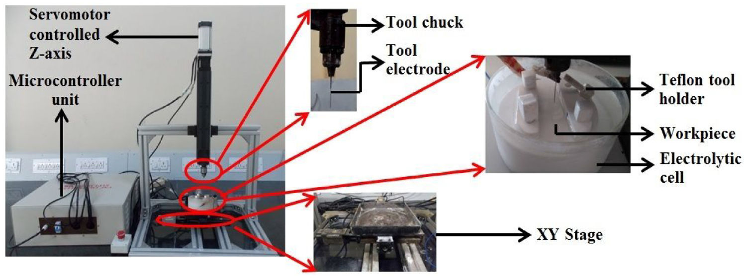
Experimental setup of the ECDM process used in the present study.
There is a possibility of misalignment caused either by the movement of the workpiece during machining or by the positional change of the tool electrode while moving it up and down repeatedly. Indeed, in the initial stages of the experiments, we observed that the tool electrode displaced the workpiece whenever there was an accidental contact between the two. The workpiece is tightly held in place using a Teflon holder to avoid this movement, as shown in Figure 1. While carrying out the experiments, we observed no change in the position of the tool electrode after repeated machining experiments. Even after moving the tool electrode “up and down” often, it is precisely positioned at the exact spatial coordinates every time after machining, which could be verified through the interface computer and tightly-held workpiece. A simple standalone traveling microscope was positioned near the workpiece-tool electrode setup. As the electrolyte was only 1 mm above the workpiece, we could observe the electrode tip position through the microscope. Further, when the electrolyte solution was periodically replenished, we could ensure that the tool electrode was positioned precisely. The tool electrode is held by a tool chuck attached to a machining head that provides movement along the Z-axis. The XY stage and the machining head are controlled by three exclusive servo motors driven by a micro-controller unit interfaced to a computer through Multi CNC® software. The experimental conditions, along with the properties of the workpiece material, are provided in Table 1.
Experimental conditions of the present study for fabricating miniature beam-mass structure on quartz substrates.
Methodology
Micro-mechanical cantilever beam-mass structures are fabricated on quartz substrates using layer-by-layer machining operation, also known as the micro-milling process. A through microstructure is obtained by machining many layers over the same area. A micro-channel with a definite width and depth is formed after machining the substrate once. The geometrical dimensions of this channel and other features such as the quality of edges and the machined surface’s smoothness are a strong function of the process parameters such as electrolyte type and concentration, tool geometry, applied voltage, Wg, and TTR. In the present study, we have fixed electrolyte type (NaOH), electrolytic concentration (30 wt.%), and tool shape (needle-shaped) for the sake of simplicity.
Experiments were conducted in two stages. In the first stage, micro-machining experiments were carried out on quartz substrates to optimize the machining voltage, TTR, and the initial Wg, as these parameters would affect the geometrical dimensions, edge linearity, and the surface quality of the machined structures. Initially, 3 mm long microchannels were fabricated at various combinations of applied voltage and TTR values and were characterized using an optical microscope (COSLABTM, India) to analyze the surface quality and measure the channel width. However, to measure the depth, cross-sections of the micro-channels were prepared and observed under the optical microscope to measure the etch depth. An optimum combination of the applied voltage and the TTR was selected by observing the machined microchannels’ quality metrics. Further, since the Wg also affects the machined grooves’ depth and width, the initial Wg has to be carefully selected based on the application of the layer-by-layer machining process.
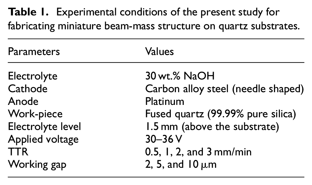
In the second stage, experiments were conducted by micro-machining a series of microchannels, each having a specific number of layers removed until a through groove is formed, as shown in Figure 2. A perspective top view is shown in Figure 2(a), and a cross-sectional view along AA′ is shown in Figure 2(b). The first channel, termed CL1, was realized by moving the tool-electrode along Y-direction and carrying out the machining operation once with the optimum initial Wg value identified at the first stage. The width and the depth of the channel were noted down. The second micro-channel CL2 was fabricated at a distance ΔX away from CL1 by carrying out the first layer of machining by following the same parameters as used for fabricating CL1 and then performing the second run by lowering the tool to a depth, termed as tool lowering depth (TLD). The value of TLD is chosen according to the Wg value required to be set between the tip of the tool and the surface of the groove. Similarly, the channel termed CL3 was formed by carrying out machining operation thrice and so on, till a through channel was formed at the “n”th time. The width and the depth of all the channels, i.e., CL1, CL2, …, and CLn, were measured using an optical micro-scope across the cross-section AA′. Finally, this information is utilized for the fabrication of the beam-mass structures on quartz substrates.
Schematic of layer-by-layer machining to fabricate an entirely through micro-channel: (a) a perspective top-view and (b) a cross-sectional view across AA′.
It is desirable to keep Wg as low as possible to achieve higher etch depth and reduce the total fabrication time. We have conducted extensive experimental investigations and observed that the MRR varies with each layer, demonstrating a decreasing trend with increasing etch depth. The reduction in MRR is primarily caused by dynamic parameters such as the electrolyte’s local temperature that varies in due course of the machining process and the lack of electrolyte flushing. Moreover, for a set of 10 experiments, the error in machining depth was around ±5 µm, which makes it extremely difficult to maintain a Wg as low as 2 µm. We have used a simple experimental setup without any feedback mechanism and cost-intensive equipment in the present work. Considering the abovementioned factors, we have used an initial Wg of 2 µm and maintained a Wg of 5 µm for machining the subsequent layers.
The beam-mass structure’s geometrical dimensions are drawn using the Draftsight™ software and fed to the Multi-CNC® module that aids the servo motors in translating it into X-, Y-, and Z-axis motions, thus fabricating the structures on the quartz substrate. We drew vertical and horizontal slicing lines separating the beam-mass structures and carried out a milling operation (three layers) along these lines. Then, the designed beam-mass structures were micromachined using the multi-pass technique to release the structures. After that, we used a diamond cutter to isolate the individual devices through slicing lines.
Results and discussion
Selection of the initial working gap
The initial Wg is a critical process parameter that requires optimization since it affects the fabricated microchannels’ width and depth. We have used a thin metal feeler gauge to set the initial working gap in the present work. The spatial coordinates of the tooltip in the ECDM setup were measured with- and without the feeler gauge. The difference in spatial coordinates (along with the Z-axis) equal to the thickness of the feeler gauge blade was used as a parameter to confirm the set working gap.
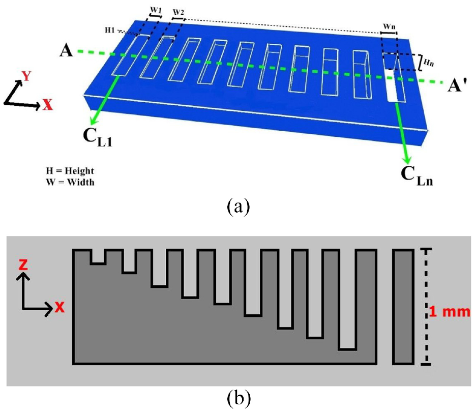
The cross-sectional views of grooves fabricated at a TTR of 1 mm/min with an applied voltage of 34 V and three different Wg values are shown in Figure 3. The reason for choosing a TTR of 1 mm/min and an applied voltage of 34 V is explained in section 3.2. The groove fabricated with a Wg of 2 µm has a width and a depth of 195 and 98 µm respectively that are greater than the grooves fabricated with Wg values of 5 and 10 µm. Initial working gaps resulting in narrow and shallow grooves would affect the electrolytic flushing during micro-machining and require more layers to remove, increasing the fabrication time for realizing through structures. For fabricating beam-mass structures, channels with linear edges with broader and deeper grooves are preferred as the linear edges improve the micro-structures’ finish, whereas a greater width is helpful in electrolyte flushing to enhance material removal. On the other hand, deeper micro-channels reduce the number of layers to be machined and the machining time of the micro-channel. Therefore, we select 2 µm as the initial Wg for the fabrication of the cantilever beam-mass structures.
Optical images of the cross-sectional views of micro-channels fabricated using a needle-shaped tool with a machining voltage of 34 V, TTR of 1 mm/min, and working gaps of 2, 5, and 10 µm.
Selection of TTR and applied voltage
The variation of the width and the depth of the micro-channels (single layer) with the applied voltage for varying values of TTR with an initial Wg of 2 µm are shown in Figure 4(a) and (b), respectively. The data points plotted in the graphs are the average of 10 samples. It is observed that the width and the depth of the machined channels increase with applied voltage due to the relative increase in temperature and thermally accelerated chemical etching. However, with increasing TTR, there is a decrease in the channel depth and width. This is primarily due to the significant reduction in the substrate’s exposure time to the spark discharges with increasing TTR.
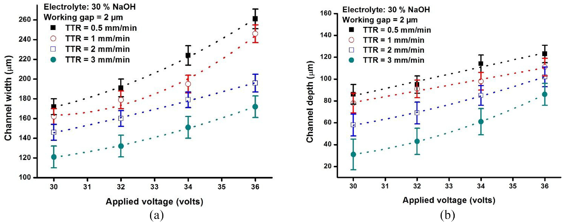
Variation of: (a) the width and (b) the depth of micro-channels fabricated using a needle-shaped tool.
In the present study, we have compared the quality of the micro-channels fabricated using tool travel rates ranging from 0.5 to 3 mm/min. Micro-channels fabricated with tool travel rates lesser than 0.5 mm/min and an applied voltage greater than 34 V resulted in thermal cracks and severe heat-affected zones. On the other hand, higher values of tool travel rates (≥3 mm/min) resulted in micro-channels with non-linear edges and stick-and-jump effect, as Abou Ziki et al. 28 reported. Due to the above reasons, tool travel rates varying from 0.5 to 3 mm/min were considered in the present study.
Optical images of the micro-channels fabricated with an initial Wg of 2 µm at various TTR and applied voltage combinations are provided in Figure 5. The channel width mentioned in the images is the average width measured across five different points along the channel’s length. Microchannels fabricated with a low TTR of 0.5 mm/min resulted in irregular edges with the heat-affected zone (HAZ) due to prolonged exposure of the substrates to the sparks. Further, with increasing applied voltage, thermal cracks can be observed, as shown in the inset provided in Figure 5(e1). On the other hand, at 2 and 3 mm/min, the channel edges are non-linear with a rough surface. The combination of the machining voltage and the TTR determines the quality of the edges and the machined surface.
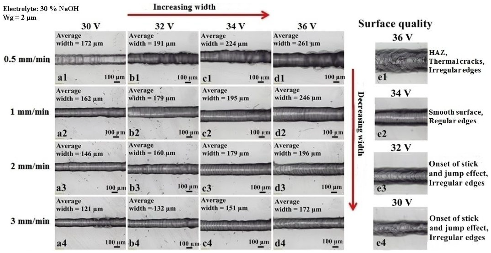
Optical images of micro-channels fabricated on quartz substrates at various TTRs and machining voltages, along with images focusing on the surface finish of a few representative microchannels.
Further, the onset of the stick-and-jump effect can also be observed at these TTR values, as evident from Figure 5(e3) and (e4), respectively. Also, for a fixed value of applied voltage, the stick-and-jump effect becomes more prominent with increasing TTR. Micro-channels fabricated with an applied voltage of 34 V and a TTR of 1 mm/min are observed to have linear edges and channels with a good surface finish. Moreover, these micro-channels are relatively wider than those realized using TTR values of 2 and 3 mm/min. As wider channels help in electrolytic flushing, we have considered a TTR of 1 mm/min, a machining voltage of 34 V, and an initial Wg of 2 µm for further studies for fabricating beam-mass structures on quartz substrates.
Fabrication of entirely through micro-channels
An entirely through microchannel can be fabricated by micro-milling operation. Even though we have used an initial Wg of 2 µm to machine the first layer, considering the experimental error with increased etch depth, a Wg of 5 µm was used for machining subsequent layers to realize completely through micro-structures.
Machining depth, Wg, and TLD
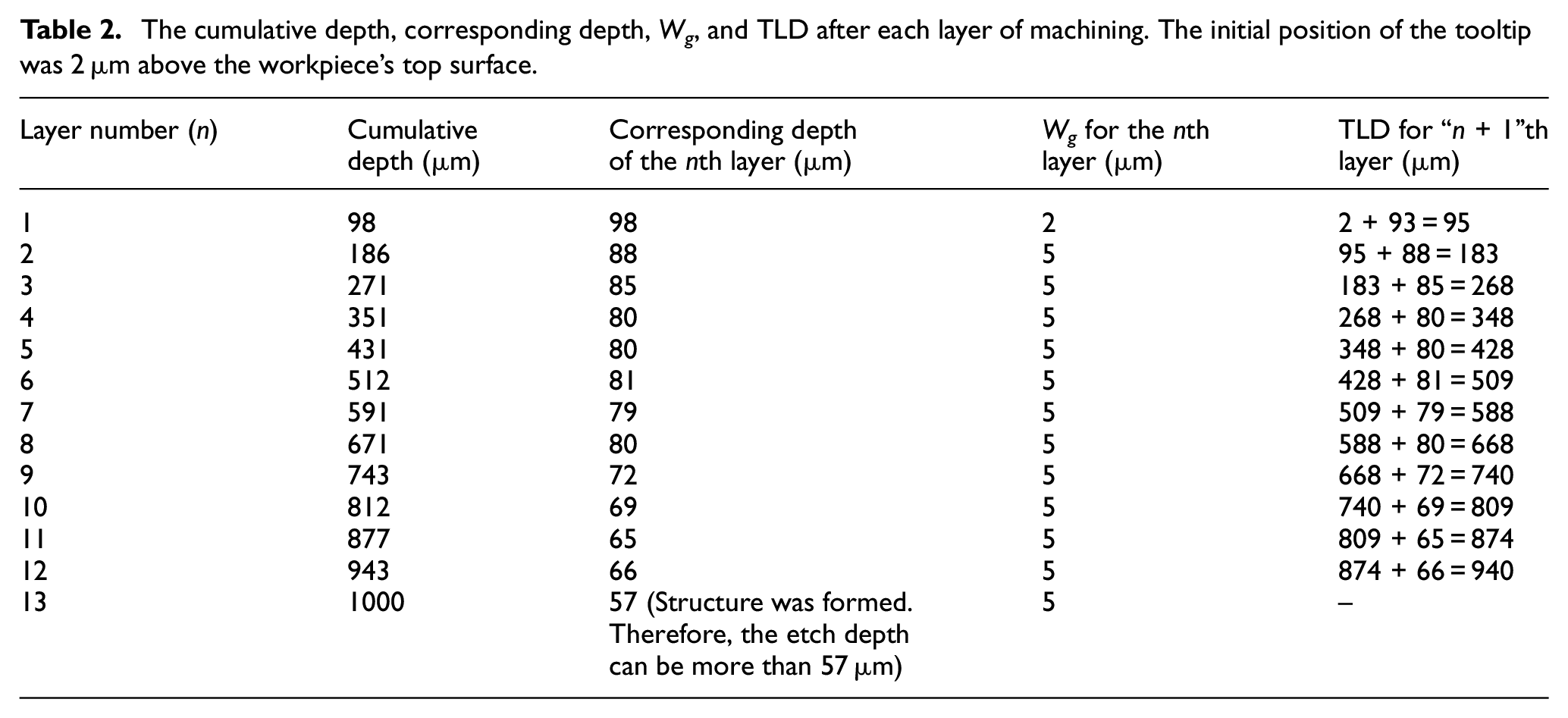
An initial Wg of 2 µm resulted in micro-channels with a depth of 98 µm. Therefore, for machining the second layer CL2 (refer Figure 2(a)), the tool was lowered (defined as TLD prior) by 95 µm from its previous position (initial gap of 2 µm + 93 µm, (etch depth of 98 µm – a working gap of 5 µm = 93 µm). The second layer machining resulted in an etch depth of 88 µm. Therefore, the tool was lowered for an overall depth of 95 + 88 = 183 µm to keep a working gap of 5 µm. The process was continued until all the layers were machined to achieve an entirely through beam-mass structure. In work reported by Mishra et al., 31 the authors reduced the tool feed rate (TFR) after removing the sixth layer, keeping all other parameters constant to increase the MRR with increasing depth. The present work’s primary contribution is measuring etch depth after each layer of micromachining in the first stage of experiments and utilizing the data in the second stage of the experiment to adjust the TLD to maintain a constant Wg of 5 µm for all layers except the first layer.
For the chosen process parameters, it is required to machine 13 layers for realizing an entirely through channel in the present work. The cross-sectional views of all the 13 channels with their corresponding etch depth are shown in Figure 6. The details of the layer number, corresponding layer depth, cumulative depth, Wg, and TLD are provided in Table 2. It is observed from the table that with increasing machining depth, the corresponding layer depth decreases, necessitating changes in TLD to maintain a uniform Wg of 5 µm. The graphical representations of the related corresponding depth, cumulative depth, and channel width are shown in Figure 7(a) and (b).
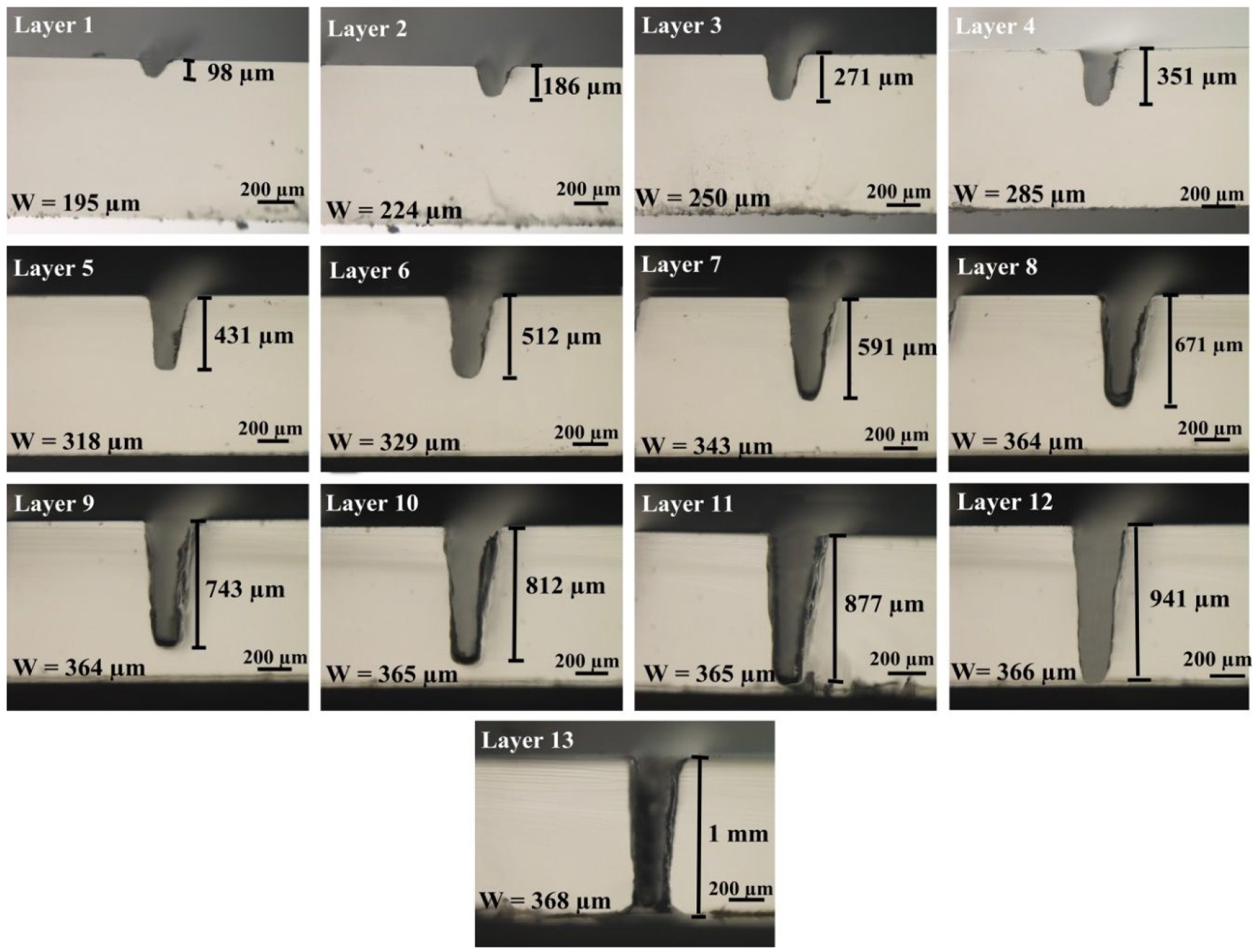
Cross-sectional view of the grooves fabricated with an initial Wg of 2 µm for the first layer and 5 µm for the consecutive layers.
The cumulative depth, corresponding depth, Wg, and TLD after each layer of machining. The initial position of the tooltip was 2 µm above the workpiece’s top surface.
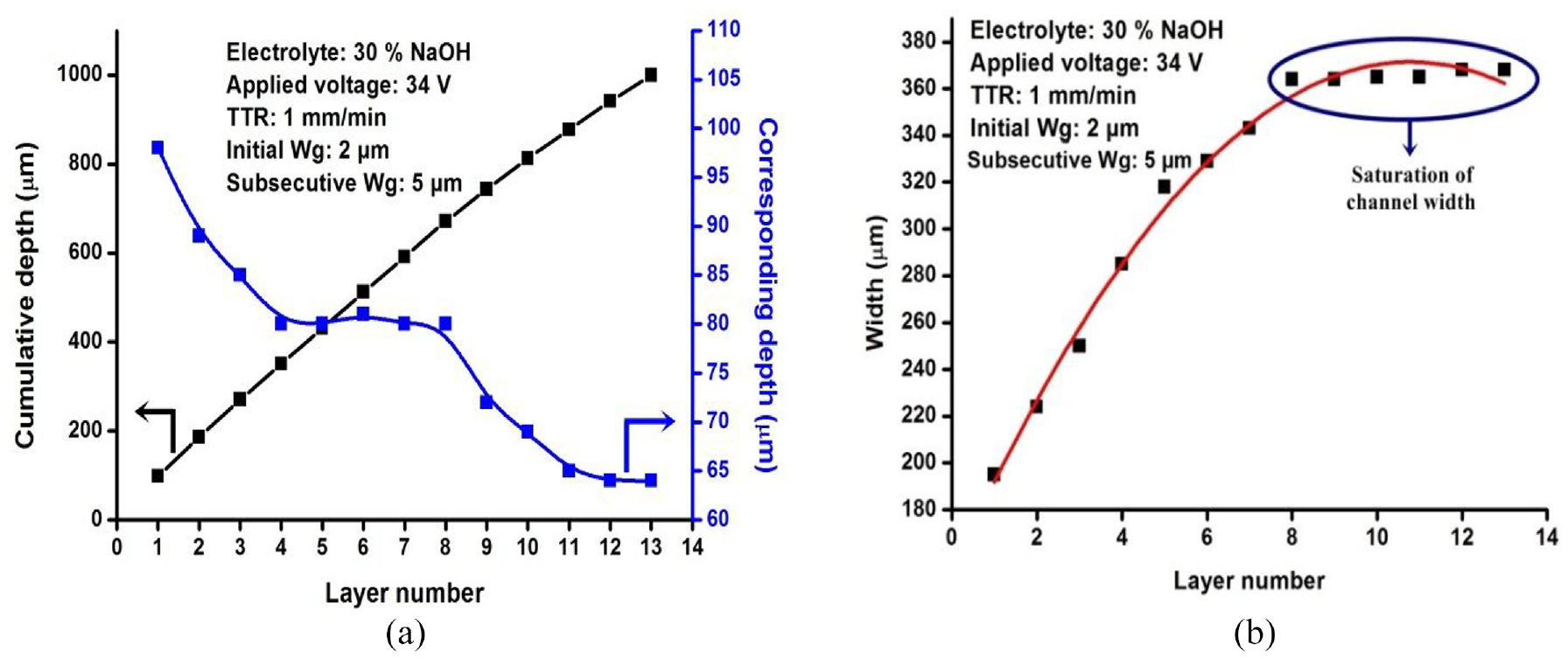
Variation of: (a) cumulative depth and corresponding depth and (b) width of the grooves after each consecutive layers of machining.
It is observed from Figure 7(a) that, even though the cumulative depth increases, the change in the plot’s slope plot depicts a reduction in MRR. The MRR was found to be 84.33 µm/layer for layers 1–4 and reduces to 80 µm/layer for layers 5–8 and further reduces to 66 µm/layer for layers 9–12. The reduction in MRR is due to the diminished electrolytic flushing, which affects chemical etching aided removal of the substrate material. This change in slope and reduced MRR are visible while looking at the corresponding depth plotted in Figure 7(a).
Width of the machined channels
The machined channels’ width is an essential aspect as it facilitates the electrolyte flow for machining the subsequent layers. In the present work, we have used needle-shaped tool electrodes for realizing beam-mass structures. A microscopic image of a needle-shaped tool electrode is shown in Figure 8, with its diameter marked at every 100 µm up to 1 mm, which is the thickness of the substrate used in the present study. The tool’s diameter is observed to increase from 89 µm at a position of 100 µm to 341 µm at a position of 1 mm. This is to say that as the machining progresses and the tool is lowered to maintain a constant Wg, the tool’s occupancy volume inside the machined hole varies. Due to this variation of the tool diameter, spark energy experienced by the walls of the drilled micro-channels would be relatively more prolonged. Due to this, with each machining layer, the drilled hole diameter varied along with its depth. The schematic of this phenomenon is depicted in Figure 9. Before machining layer 4, the groove had a depth of 271 µm and an entrance diameter of 250 µm. After machining layer 4, the groove width is increased to 285 µm with an increase of 80 µm in depth. The width of the grooves after machining each layer is plotted in Figure 7(b).
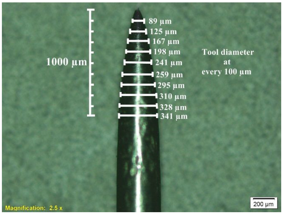
An optical image of a needle-shaped tool electrode with its diameter measured at every 100 µm along its length up to 1 mm.
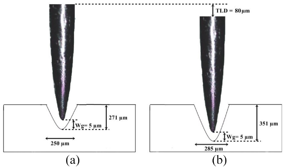
Schematic of layer-by-layer machining showing the scenario of the tool electrode: (a) before and (b) after the micro-machining of layer 4.
Fabrication of a planar beam-mass structure on a 1 mm thick quartz substrate
Based on the experiments carried out in the first two stages, we have chosen the following process parameters to fabricate planar beam-mass structures on quartz substrate: applied voltage of 34 V, TTR of 1 mm/min, initial Wg of 2 µm, and a subsequent Wg of 5 µm. The layout of the micro-mechanical structure of perimeter 9.35 mm was drawn using the DraftSight™ software as shown in Figure 10(a), and the design was fed into the Multi CNC® software. It requires 121.55 min to fabricate the structure at the 13th layer for a TTR of 1 mm/min. A Scanning Electron Microscopic (SEM) image of a fabricated device is shown in Figure 10(b) with close-in views of X, Y, and Z. It is observed from the figure that the realized structure exhibits sharp convex corners and rounded concave corners. The mass and beam walls are slanted outwards primarily because of the needle shape tools used for machining.
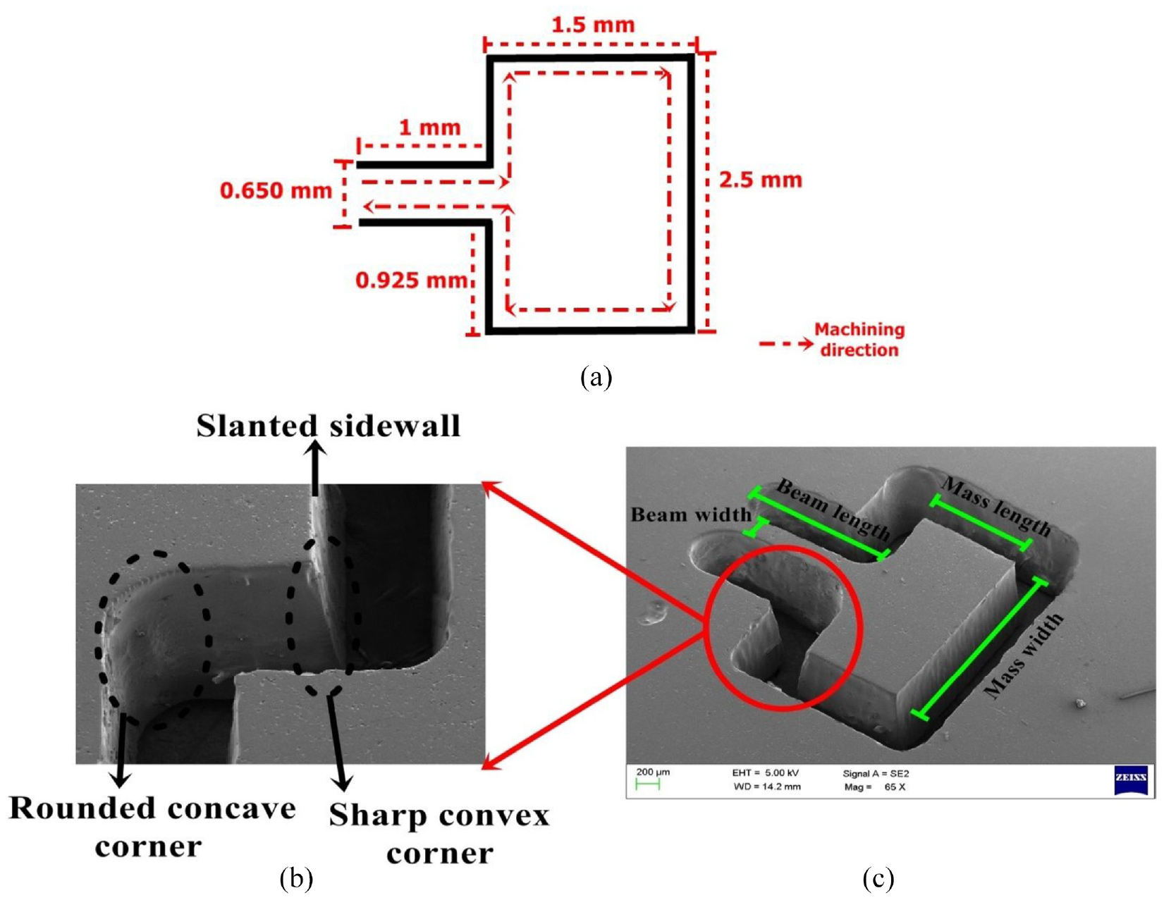
(a) Layout of a 2.5 mm × 2.5 mm beam-mass structure and (b) SEM image of a fabricated 2.5 mm× 2.5 mm beam-mass structure.
The top and bottom views of the device captured using an optical microscope are shown in Figure 11, with the geometrical dimensions measured using an integrated micro-meter. The designed and the measured width (top view) of the beam are 650 and 249 µm, respectively. The beam’s actual width reduction from the designed value is due to the overcut caused by the tool on either side of the beam while repeatedly machining to realize the beam-mass structure. Further, the beam’s width is 380 µm at its bottom surface, as shown in Figure 11(b). The difference in the width between the top and bottom surfaces is due to the slanting wall caused by the needle-shaped tool.
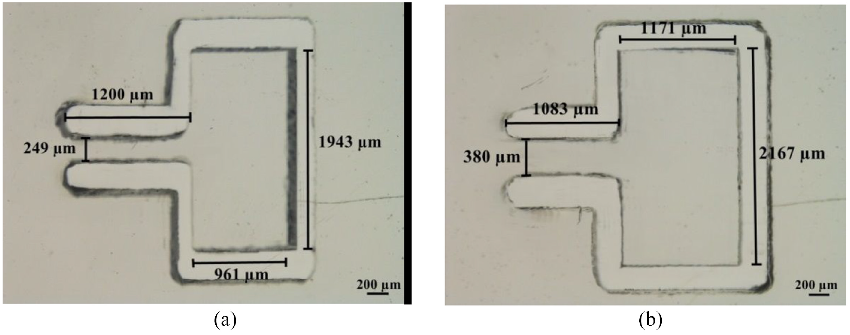
Optical microscope views of the fabricated beam-mass structure: (a) the top and (b) the bottom view.
We have fabricated three more beam-mass structures with a relatively smaller overall dimension of 2 mm × 2 mm and three different beam widths. The structures’ perimeters are 7.2, 7.4, and 7.5 mm for the structures with a layout beam width of 0.8, 0.6, and 0.4 mm, respectively. It takes around 93–98 min (depending on the perimeter) to fabricate these devices compared to the 2.5 mm × 2.5 mm devices that require 121.55 min for their fabrication. The layout diagrams of these devices with the geometrical structures are shown in Figure 12. The measured widths at the top surface of the three structures are 440, 251, and 81 µm, respectively. The beam’s width, proof mass’s length, and width are reduced in the fabricated structures compared to their layout dimensions, whereas the beam’s length increased after fabrication. These changes in geometrical dimensions of the micro-mechanical structures are primarily due to the overcut caused by the tool electrodes during the multi-layer machining process. The average reduction in the beam width, the proof mass length, and the three fabricated devices’ proof mass width are 359, 363, and 400 µm, respectively. The average increment in the length of the beam is found to be 186 µm.
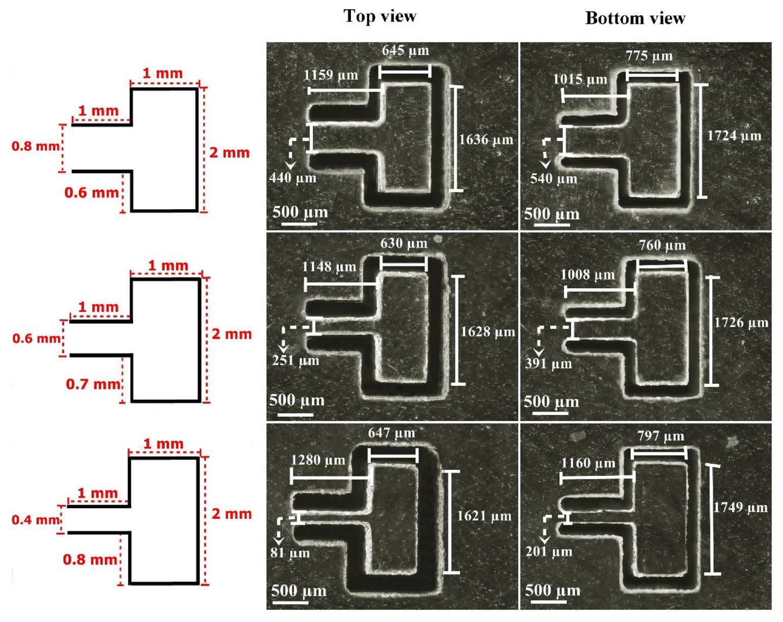
Designed and fabricated images of the beam-mass structures of different beam widths.
The device-to-device variation of the geometrical features across the devices is mainly because of the following reasons:
In the present study, the electrolytic level maintained above the substrate surface is about 1.5 mm at a 30 wt.% NaOH concentration with the experiments conducted at room temperature. At a TTR of 1 mm/min, it takes around 9.35 min for one layer of micro-machining. During this period, due to localized heating, the electrolyte above the substrate surface evaporates, altering the concentration, level, and temperature of the electrolytic solution in the machining cell, thereby changing the machining characteristics. It is challenging to estimate the exact amount of the solution that must be replenished to supply the loss of the electrolyte due to evaporation and maintain the concentration and the level of the electrolyte above the substrate surface, same throughout the machining process. Maintaining a constant temperature of the electrolyte throughout the machining process is an equally challenging task.
Another critical parameter is the flatness of the workpiece, which can be affected by the substrate holder’s slightest slope, the surface on which the setup is placed, or even the profile of the substrate itself. The workpiece’s slope would lead to a difference in the Wg along the path traveled by the tool electrode during the machining process, which causes dimensional variations across the machined structures. Further, the tool electrode’s eccentricity clamped to the tool chuck also affects the sidewall’s slope and the dimensions of the fabricated structure. It is necessary to ensure that the tool is clamped perpendicularly without any tilt.
It is to be noted that the results obtained in the present study hold good for the parametric conditions considered. The results would vary with the applied voltage, initial and subsequent working gaps, TTR, electrolytic type and concentration, substrate and tool material, and tool shape. For example, using a higher value of machining voltage would result in grooves with wider entrance diameters with relatively more depth. Wider entrance diameters would allow more electrolytic solution inside the channels, which is very useful, especially when the machining enters the hydrodynamic regime. Achieving more depth per layer also helps in reducing the overall fabrication time of the devices. We have used needle-shaped tools made of carbon alloy steel material for fabricating the devices primarily for mechanical strength. A few other reported tool shapes in the ECDM literature are cylindrical, 33 one-side flat, 34 core drill tool, 35 and spherical-tip22,25 tools. Machining process efficiency can be improved by using these tools. The addition of surfactants 10 to an electrolytic solution effectively reduces the critical voltage of an ECDM process. By adding surfactants, the machining voltage of the process can also be reduced. One more recent method proposed to improve the machining efficiency is to use a tool with sidewall insulator coating. 36 All the techniques mentioned above would alter the machining dynamics and lateral geometrical dimensions of realized micro-structures.
Conclusion
In the present work, we have presented the fabrication of a micro-mechanical planar cantilever beam-mass structure on 1 mm thick quartz substrates using the layer-by-layer machining technique of an ECDM process. Initially, the process parameters such as TTR and the applied voltage were optimized to fabricate deeper and wider micro-channels to facilitate electrolyte flushing. An array of micro-channels with varying depths was fabricated with the optimized process parameters until an entirely through micro-groove was obtained. Using the details such as channel width, cumulative depth, and corresponding depth after each layer was removed, the initial Wg for fabricating the first channel and the Wg value for fabricating the subsequent layers were identified. An applied voltage of 34 V, TTR of 1 mm/min, an initial Wg of 2 µm, and a gap of 5 µm for fabricating the subsequent layers were chosen. Later, with the selected parameters, a 2.5 mm × 2.5 mm beam-mass structure was fabricated on a thick quartz substrate. A fabricated device had a minimum beam width of 81 µm with a sharp convex corner and rounded concave corners.
Footnotes
Acknowledgements
We thank Dr. K. Mohan, School of Civil Engineering of VIT Chennai, for his help in extending the measurement facilities, Mr. Swaroop, a doctoral scholar of the research group, for his help in the artwork of a few figures.
Declaration of conflicting interests
The author(s) declared no potential conflicts of interest with respect to the research, authorship, and/or publication of this article.
Funding
The author(s) disclosed receipt of the following financial support for the research, authorship, and/or publication of this article: This work is supported through the internal funding of the Vellore Institute of Technology, Chennai (VIT Chennai).